HAL Id: in2p3-00161423
http://hal.in2p3.fr/in2p3-00161423
Submitted on 10 Jul 2007
HAL is a multi-disciplinary open access
archive for the deposit and dissemination of
sci-entific research documents, whether they are
pub-lished or not. The documents may come from
teaching and research institutions in France or
abroad, or from public or private research centers.
L’archive ouverte pluridisciplinaire HAL, est
destinée au dépôt et à la diffusion de documents
scientifiques de niveau recherche, publiés ou non,
émanant des établissements d’enseignement et de
recherche français ou étrangers, des laboratoires
publics ou privés.
14-Bit and 2GS/s Low Power Digitizing Boards for
Physics Experiments
D. Breton, E. Delagnes
To cite this version:
D. Breton, E. Delagnes. 14-Bit and 2GS/s Low Power Digitizing Boards for Physics Experiments.
2006 IEEE Nuclear Science Symposium, Medical Imaging Conference, and 15th International Room
Temperature Semiconductor Detector Workshop, Oct 2006, San Diego, United States. IEEE, 2,
pp.990-995, 2006, �10.1109/NSSMIC.2006.356012�. �in2p3-00161423�
Dominique Breton and Eric Delagnes
Manuscript received November 27, 2006.
Dominique Breton is with CNRS/LAL, BP34, 91898 Orsay, France, (corresponding author) e-mail: [email protected]. Eric Delagnes is with CEA/DSM/DAPNIA/SEDI, 91191 Gif-sur-Yvette Cedex, France, e-mail: [email protected].
Abstract– The trend in data acquisition systems for modern physics experiments is to digitize analog signals closer and closer to the detector. The digitization systems have followed the progress of commercial analog to digital converters. The state of the art for these devices is currently 200 MSample/s for a 14-bit range. The new boards, described in this paper, have been designed to improve these performances by more than an order of magnitude. This board mainly includes 4 channels sampling analog data up to 2 GSamples/s with an analog bandwidth of 300 MHz, and digitizing it with a 14-bit dynamic range. It is based on the custom-designed MATACQ chip. The latter’s innovative design permits reaching these performances with power consumption smaller than 1W, thus allowing a total consumption below 20W for the whole board. The board is triggerable either by internal or external signals and several boards are easily synchronizable. The board integrates USB, GPIB and VME interfaces that permit a readout speed of up to 500 events/s with the whole memory depth of the 4 channels read.
I. INTRODUCTION
HE trend in data acquisition systems for modern physics experiments is to digitize signals closer and closer to the detector. It offers more flexibility for online or offline treatments and is particularly useful in the prototyping or early phases of the experiments. Commercial digitization boards have followed the evolution of ADC technologies and are today available with sampling frequencies of a few hundred MSample/s for a 10-bit to 12-bit resolution. ADC chips with higher performances (8 12-bits to 10 bits at 2 GSample/s) have been developed, mainly for military applications. But they are expensive, difficult to purchase and to implement and exhibit huge power consumption (5 W to 10 W for the sole ADC chip). Moreover, as the data rate at the ADC output is as high as 10 Gbit/s, it is mandatory to use very fast memories or very fast in-flight treatment digital electronics that are also expensive and power consuming. In addition, most of the hardly converted signals will be thrown away right after for it is impossible to store such amounts of data over a long period of time. Other commercially available solutions, less compact, based on interleaved lower speed ADCs suffer
from the same cost and power consumption limitations. For these reasons, the available commercial boards offering sampling frequencies higher than 1 GSample/s are all limited to dynamic ranges below 10 bits, and to a modularity of only 1 or 2 channels per board. These boards are expensive and several boards are not easily synchronizable, so that their use in multichannel systems is difficult. Yet, there are important needs, particularly in physics experiments, for digitization systems covering a high dynamic range with sampling frequency higher than one GHz and a rather short recording depth. In association with fast detectors, they can be used for timing, pulse shape discrimination and charge measurement even in a high rate or high background environment. The MATACQ14 board described here has been developed especially for this purpose. It is built around the MATACQ chip, an analog memory described below, as it was also the case for the former 12-bit version called MATACQVME [1].
II. DESCRIPTION OF THE MATACQCHIP
The MATACQ chip is a circular buffer based on a new and innovative matrix structure. It was originally designed in the inexpensive AMS CMOS 0.8 µm technology. It makes use, as some former fast analog sampler chips [2], [3], [4] of an array of switched capacitors associated with Delay Locked Loops (DLL). But, thanks to its new matrix structure, its memory depth has been extended to more than 2500 samples.
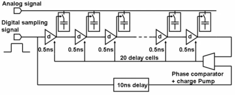
Fig. 1: Principle of the DLL
14-Bit and 2GS/s Low Power Digitizing Boards
for Physics Experiments
As in the previous chips, the 2 GHz sampling frequency is achieved with an input clock frequency of only 100 MHz thanks to the virtual frequency multiplication by DLLs. An example of the corresponding principle is described on Fig. 1. A digital pulse propagates along a chain of 20 individual 0.5 ns delays. All of them can be finely tuned through an analog voltage command. Their respective outputs are connected to the sampling command input of analog memory cells.At the output of the last delay, the phase of the sampling edge is compared to the phase of the input pulse delayed by 10 ns. The phase comparator then produces an analog voltage which is used to servo-control the chain of delays.
As shown on Fig. 2 and Fig. 3, the MATACQ chip is mainly a matrix constituted of 128 sampling DLL like the one of Fig. 1, but arranged in columns. The DLL digital input pulses actually correspond to the successive outputs of a main shift register clocked by the 100 MHz clock reshaped in dedicated blocks. The 10 ns precise delay of each D.L.L is provided by a second shift register (called “reference”) where the pulse is delayed by one clock period compared to the first register. During every clock period, the pointer propagates inside a new column, thus covering the full matrix after a while. After having reached the end of the last column, it comes back to the top of the first one.
To eliminate crosstalk between the lines, an input buffer is located between the common analog input and each line. Thus no effect of a switch sampling the signal on a given line can be seen on the next line which will get sampled right after. Moreover, for the same bandwidth, the total power dissipation is lower than with a single global input buffer.
In order to ensure the stability of the servo-control, the DLL has a limited frequency range of operation, typically ranging between 700 MSample/s and 2.5 GSample/s, making it impossible to sample at lower frequencies.
Fig. 2: Principle of the MATACQ chip.
To overcome this limitation, the so-called validation registers can possibly be used to mask some chosen lines during the sampling operation, this thanks to an AND-gate
located in each analog-memory-cell command circuit. After the write pointer has reached the end of the matrix, these registers are shifted. Depending on the initial value of the validation registers, this permits reducing the acquisition frequency by a factor 2 to 20 without reducing the memory depth.
Fig. 3: The MATACQ chip layout. It contains 100,000 transistors on a 30 mm2 silicon die. The 2560-cell switched capacitor array covers 80% of the chip area.
The input buffers are the most difficult elements to design on the chip. Their own bandwidth, more than that of the memory cells, is the main limitation to the overall bandwidth. They are the main power consumers in the chip. Their bandwidth, and thus the global chip power consumption, is actually programmable by slow control: 1 W for 300 MHz, ½ W for 250 MHz, ¼ W for 200 MHz, below 100 mW in stand-by mode. In order to save power, the amplifiers may also be turned off during the read-out operation of the matrix.
The acquisition is stopped upon reception of a stop signal. The latter derives from an asynchronous trigger signal which is also dated inside the chip by a Time to Digital Converter (TDC) based on a counter and an analog ramp interpolator, with a measurement step of 12 ps.
The analog data is then read in parallel column by column by the read-out amplifiers located on each line, and multiplexed towards an external 14-bit ADC. This can be done either from the first column to the last, or from the column where acquisition was stopped, thus allowing a partial and selective readout of the memory.
As the amplifiers of each line have individual offsets, the pedestal of each line has to be calibrated. This calibration remains valid for months.
This chip has been designed using techniques and structures originally developed for the ATLAS Liquid Argon Calorimeter (LARG) analog memory [5], thus
allowing the new design to conserve a wide dynamic range of almost 14 bits.
III. DESCRIPTION OF MATACQ14 BOARD
A. MATACQ14 board overview
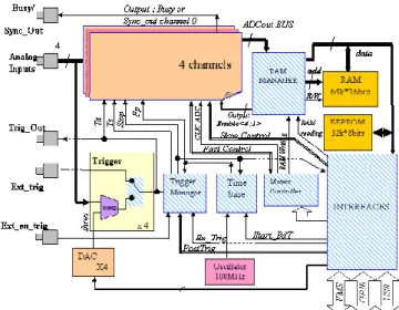
The MATACQ14 board (see Fig. 4 and Fig. 5), based on several MATACQ chips, is suited for precise acquisition of fast analog signals. It performs the coding of 4 analog channels with a bandwidth of up to 300 MHz and over a 14-bit dynamic range, at a sampling frequency (Fe) ranging between 50MHz and 2 GHz and over a depth of 2520 usable points. This board, in the mechanical format VME 6U is compatible with several standards of acquisition (VME A32/D32, A24/D16, GPIB, and USB 2.0). Almost all the board digital electronics is located inside a unique FPGA, of which the configuration EEPROM can be reprogrammed thanks to a JTAG connector. The FPGA provides the bus interfaces, the control of the MATACQ chips, of the event RAM and of the calibration EEPROM, the time-base and the trigger logics.
Fig. 4: Synopsis of the MATACQ14 board.
The board makes use of a 10-layer PCB, where power and ground planes have been carefully designed. All critical analog and digital signals are sent to the MATACQ chips over differential low level and controlled impedance lines. Special care has been taken to avoid any type of crosstalk between the digital and analog parts.
The clock source is a 100 MHz oscillator. However, an external clock may be used for special purposes. A second oscillator provides a random clock for the trigger system.
The input analog signals cover the +-1V range. The whole acquisition chain is DC coupled.
As shown on Fig. 6, the acquisition is realized in three phases:
-Acquisition: the analog signal is continuously sampled at the sampling frequency Fe in the MATACQ circular analog
memory. The arrival of a trigger signal initiates the stopping phase of the sampling. At the end of this phase, the state of the memory is latched: it then contains the last 2560 points sampled (of which 2520 are valid).
Fig. 5: The 4-channel MATACQ14 board.
-Digitization and storage: upon reception of the order to stop the acquisition, the samples stored under analog form in the MATACQ chips are read out rapidly (650 µs for 4 full channels) and coded into digital data over 14 bits, then stored in the event RAM. The acquisition is then informed of the end of the coding phase by an interruption (it may also scan a flag within an internal register).
Fig. 6: Data flow in the MATACQ14 board.
- Reading: the RAM can then be read out by the acquisition system. For an acquisition system based on VME A24-D16 standard, this operation lasts a few ms for the full readout of a 4-channel board. This permits to reach an acquisition frequency of a few hundred Hz for the readout of 2500 points per channel. Using the 32-bit readout mode, a rate of 500 acquisitions of all the cells over the 4 channels is reachable. With standard GPIB and USB 2.0, rates above 50 Hz are also possible. A special readout mode, allowing the user to transfer selectively only a subset
of the memory permits increasing the acquisition rate if necessary.
An input for a 1-PPS GPS clock is available on the front panel in order to permit an absolute datation of the events. B. MATACQ14 board triggering
Several modes of triggering are available on this board (see Fig. 7). Each analog input is sent to a comparator receiving an individual DAC-programmable threshold. Each output of these comparators or any logical-OR combination of them can be used to trigger the board. This can also be done through an external input, compatible with both ECL and NIM levels. Several MATACQ14 boards can also be synchronized by using a common external trigger. This signal can be built externally from the “Trig_Out” output available on each board.
Fig. 7: The first level trigger selection tree.
A second level trigger is also available as shown on Fig. 8. It permits making a pause in the acquisition and either converting the data or going back to acquisition within a user-defined time window. This may help saving a lot of dead-time in applications where data can be validated within a reasonable time after their sampling.
Fig. 8: The second level trigger.
The position of the 2500-point acquisition window relatively to the trigger is programmable over a 655 µs range. The on-chip interpolation system (see Fig. 12) tags the trigger with steps of 12 ps, much smaller than the sampling period, thus allowing a good synchronization
between channels or boards, and consequently the adequate use of this board in time measurement experiments. Moreover, it also permits performing acquisitions in equivalent time mode for repetitive signals like with an oscilloscope.
C. MATACQ14 board performances
Fig. 9 shows the result of a one-shot baseline acquisition performed over the 4 channels located in the same board. The plots are superimposed. It shows a noise value of about 175 µV rms which, combined with the 2V maximum range, confirms the dynamic range of 13.5 bits rms.
Fig. 9: One-shot acquisition of the baseline of the 4 channels.
Fig. 10 shows a simple one shot acquisition of a 10 MHz sine wave signal. One can appreciate how smooth the signal appears thanks to the 14-bit signal to noise ratio when compared to the same signal sampled with an expensive 8 bit oscilloscope as shown on Fig. 11.
Fig. 10: Acquisition of a 10 MHz 0.8 V peak-peak sinewave with the MATACQ14 board.
Fig. 11: Acquisition of the same 10 MHz 0.8 V peak-peak sinewave with a high-end (2002), commercial 10 GSample/s oscilloscope.
The integral and differential non-linearities of the board were measured using the pulses (10 MHz of equivalent bandwidth) of the ATLAS Liquid Argon Calorimeter (LARG) calibration board. The differential values are smaller or equal to half a LSB of the ADC, well within +/- 0.5 per mil of the full tested range, whereas the integral non-linearity remains within 2 LSB. This includes the contributions of the MATACQ14 board and of the calibration board plus the one of the ATLAS LARG shaper used.
A main element of the datation chain is the interpolator integrated in the MATACQ chip. Fig.12 shows the block diagram of the latter, and the distribution of the interpolators of the 4 channels at 2GS/s. They display a flat shape with sharp edges, which is the main requirement for a good time precision.
Fig. 12: synopsis of the interpolator and distribution of the values of the 4 channels at 2GS/s.
Several different types of jitter can actually be distinguished inside the board: the clock jitter, the sampling jitter of the MATACQ chip, and the jitter of the trigger and datation chain. The convolution of all of them leads to an overall jitter of 60 ps rms. The latter is dominated by the clock and trigger chains in the range of 50 ps rms as displayed on Fig. 13.
Fig. 13: Distribution of the absolute sampling time on a given channel (steps of 10ps in X, rms jitter of 53ps).
The sampling jitter is much smaller. It can be evaluated from the distribution of the sampling time difference between two different channels of the same board simultaneously fed with the same signal, as displayed on Fig. 14. The extracted rms jitter per channel is indeed of only 20 ps. This permits performing accurate time measurements between channels, and even precise absolute datation if the trigger threshold crossing of the triggering channel is interpolated from the acquired data.
Fig. 14: Distribution of the sampling time difference between two channels (steps of 10ps in X, rms jitter of 17ps).
Another important feature of the board is its ability to perform an FFT on a single acquisition thanks to its high SNR and very good linearity. Fig. 14 shows the result of an FFT measurement on a 10 MHz sine wave with no clock harmonic or spurious frequency above -65 dB.
The effective number of bits (ENOB) was measured on the same sine wave. The SNR was first extracted as the power ratio between the fitted sine wave and the residues. Then the ENOB was calculated using the usual formula (1):
ENOB = (SNR-1.76)/6.02 = 8.7 bits. (1)
Fig. 14: FFT on a single 10-MHz 1Vp-p sine wave acquisition.
This is almost totally dominated by the contribution of the 20 ps rms sampling jitter. The latter’s theoretical
0.0 -120.0 -115.0 -110.0 -105.0 -100.0 -95.0 -90.0 -85.0 -80.0 -75.0 -70.0 -65.0 -60.0 -55.0 -50.0 -45.0 -40.0 -35.0 -30.0 -25.0 -20.0 -15.0 -10.0 -5.0 Frequency (Hz) 1.0G 1.0M 10.0M 100.0M
contribution to the SNR calculated using (2) is indeed 58 dB, corresponding to an ENOB of 9 bits.
SNR = -20 . Log ( 2 . π . fsin . σt) (2)
Where fsin is the sine wave frequency in Hz and σt is the
sampling jitter in s rms.
For information, the ENOB calculated in the same conditions for the data of Fig. 11 is 5.0 bits.
TABLE I
MAIN PERFORMANCE AND CHARACTERISTICS OF THE MATACQ14 BOARD
This value may limit the application field of the board. However, the ENOB does not describe the board’s ability to measure both big and tiny signals at the same time, or to finely discriminate and date piled-up signals, which are the main domains of application aimed at. The jitter value of 20 ps is mainly limited by the matrix structure of the sampler, and could hardly be greatly improved, for example by trying to improve the clock distribution.
The main characteristics and performances measured on the board are summarized in Table I. All the jitter measurements have been performed at 2 GSample/s.
TABLE II
POWERCONSUMPTION OF THE MATACQ14 BOARD
The power supply information is summarized in Table II. Except the +-5V for the analog amplifiers regulated from the +-12V inputs, all the power supplies derive from the +5V via DC-DC converters and low dropout regulators. This ensures very low charge current on the +-12V and overall power dissipation, i-e 13W in standard mode and 20W in peak mode (waiting for trigger.
IV. EXAMPLES OF APPLICATIONS
There are currently a lot of applications of the MATACQ14 board. Most of them are gathered within three main fields:
- Timing measurement in very high-rate or noisy environments.
- Test benches for fast detector or electronics chains characterization.
- Pulse shape identification and measurement.
V. CONCLUSION
A new VME board based on the MATACQ ASIC has been designed. It offers a sampling frequency up to 2 GS/s over 4 channels, a 14-bit dynamic range and a memory depth of more than 2500 samples/channel with a sampling jitter of 20 ps rms. These performances, not available together in any other commercial board, make it adequate for a wide range of applications in test benches or physics experiments where the needed acquisition rates do not exceed 500 Hz. This design will soon be transferred to an industrial partner and thus be commercially available.
REFERENCES
[1] D. Breton, E. Delagnes, and M. Houry, “Very High Dynamic Range and High Sampling Rate VME Digitizing Boards for Physics Experiments”, IEEE Transactions on Nuclear Science, December 2005, volume 52, number 6, pp. 2853-2860
[2] G. Haller and B. A. Wooley, “ A 700 MHz Switched Capacitor Analog Waveform Sampling Circuit”, IEEE journal of solid state circuits, vol. 29, no 4, pp. 500-508, April 1994.
[3] S. Kleinfelder, University of California, Berkeley, 1992 Thesis: “A Multi-Gigahertz Analog Transient Waveform Recorder Integrated Circuit“, Thesis for M.S. in Electrical Engineering and Computer Science, 1992.
[4] D. Lachartre and F. Feinstein, “Application Specific Integrated Circuits For Antares Offshore Front-End Electronics”, Nucl. Instrum. Meth. A442:99-104, 2000.
[5] D. Breton, J. Ardelean, E. Auge, R. Bernier, M. Bouchel, B. Lavigne, G. Martin-Chassard, E. Plaige, J.J. Veillet, E. Delagnes, and M. Huet “A 16 Bit-40 Mhz Readout System Based On Dual Port Analog Memories For LHC Experiments”, Proceedings Of The 2nd Workshop On Electronics For LHC Experiments, Balatonfüred (Hungary), Sept 96. SUPPLY OPTIMUM VOLTAGE STANDARD CURRENT PEAK CURRENT UNIT +5V +5V 1.5 3.0 A +12V +7.5V 0.32 0.32 A -12V -7.5V 0.14 0.14 A
NAME QUANTITY UNIT
INPUT IMPEDANCE 50 OHM DYNAMIC RANGE +/- 1 V DIGITIZATION LSB 125 µV
NOISE <180 µV RMS ANALOG BANDWIDTH 300 MHZ HARMONIC DISTORSION FOR A 10MHZ INPUT <65 dB
INTEGRAL NON LINEARITY <2 LSB DIFFERENTIAL NON LINEARITY <0.5 PER MIL
SAMPLING FREQUENCY 50 TO 2000 MHZ SAMPLING JITTER <20 PS RMS CHANNEL TO CHANNEL JITTER <30 PS RMS TRIGGER CHAIN JITTER <50 PS RMS OVERALL JITTER <60 PS RMS