HAL Id: hal-01876565
https://hal.archives-ouvertes.fr/hal-01876565
Submitted on 28 Jan 2020
HAL is a multi-disciplinary open access
archive for the deposit and dissemination of
sci-entific research documents, whether they are
pub-lished or not. The documents may come from
teaching and research institutions in France or
abroad, or from public or private research centers.
L’archive ouverte pluridisciplinaire HAL, est
destinée au dépôt et à la diffusion de documents
scientifiques de niveau recherche, publiés ou non,
émanant des établissements d’enseignement et de
recherche français ou étrangers, des laboratoires
publics ou privés.
An Insight into Space Charge Measurements
P. Notingher, S. Holé, Laurent Berquez, G. Teyssedre
To cite this version:
P. Notingher, S. Holé, Laurent Berquez, G. Teyssedre. An Insight into Space Charge Measurements.
International Journal of Plasma Environmental Science and Technology, Institute of Electrostatics
Japan, 2017, 11 (1), pp.26-37. �10.34343/ijpest.2017.11.01.026�. �hal-01876565�
1Institut d’Electronique et des Syst`emes (IES), UMR 5214 CNRS / Universit´e de Montpellier, France
2Laboratoire de Physique et d ´Etude des Mat´eriaux (LPEM), UMR 8213 CNRS / Universit´e Paris 6 / ESPCI-Paris Tech, France 3Laboratoire Plasma et Conversion d’Energie (LAPLACE), UMR 5213 CNRS / Universit´e de Toulouse, France
Abstract—This paper aims at giving an insight into the field of non-destructive methods for localizing and quantifying electric charges and field distribution in dielectrics. The fundamentals of the influence (or “stimuli”) methods used for measuring space charge and polarization distributions in solid insulating structures are first presented. The possibilities offered today by these methods and their fallouts in the domains of dielectric materials, electrical engineering and electronics structures are then put into evidence using various supporting examples. Experimental set-ups and results obtained in recent years are reviewed, and perspectives of evolution of these methods are discussed. Challenges and expected achievements in the near future are brought into focus.
Keywords—Space charge, electric field, dielectric, insulator, non-destructive method
I. INTRODUCTION
The development of charge-based or charge-controlled de-vices needs a perfect knowledge of the amount and of the distribution of the electric charge in the different material lay-ers and at their interfaces. This need is particularly acute when high electric fields establish in the structures during operation, as in electrets, MEMS, devices for controlling micro-fluids in lab-on-a-chip, high-voltage high-current integrated devices, micro-electro-thermal heat sinks for micro components etc.
On the other hand, electrical charge accumulation in di-electrics (or space charge, as it is commonly referred to) can have dramatic effects when uncontrolled. Thus, the electric field induced by the development of space charges is su-perimposed to the geometrical electric field applied to the material in its usual operating conditions. The resulting value of the field can approach and even exceed the breakdown threshold, leading to an alteration or to the destruction of the material and, as a consequence, to a possible failure of the system in which it is included [1]. The risk is increased when high electric fields are applied to the component, at the interface between different materials, or in the presence of external factors able to induce significant amount of charges in the insulating layers (e.g. radiations). Even without reaching breakdown, the charges accumulated in the insulating layers of a device may provoke malfunction affecting system reliability. This is a critical problem in contexts with considerable eco-nomical dimensions and where human security considerations are essential, such as in electrical power transport, airborne and space applications.
Determining the charge density and field values and distri-butions is therefore an important matter, both for designing efficient sensors and for optimizing dielectric materials and structures. Non-destructive measuring techniques are
prefer-Corresponding author: Petru Notingher
e-mail address: [email protected]
Presented at the 3rd ISNPEDADM 2015 (New electrical technologies for environment), in October 2015
able because the evolution of the charge distribution under real operating conditions can be monitored. This has led to the development, over the last decades, of several non-destructive charge measurement techniques, commonly known as “influence methods” or “stimuli methods” [2]–[16]. These methods are based on the application of a mechanical, a thermal or an electrical stimulus which slightly perturbs the electrostatic equilibrium of the measured sample, giving birth to an electrical or mechanical transient response which allows determining the electric field and charge distributions across the sample.
As they are direct, non-destructive and of potential high resolution, the stimuli methods can bring important informa-tion when used alone or in combinainforma-tion to other techniques. Historically, the stimuli methods have been used for a wide variety of electrical engineering applications involving thick insulating layers (> 100 µm). This is still a very important matter, with the challenge of being able to determine the real field distribution in full-size structures for high voltage applications. On the other hand, increasing interest is now given to the application of stimuli methods to thin layers (< 1 µm) and electronic structures [16], [17], as the classical methods used in micro-electronics are either destructive or of insufficient resolution. Another emerging domain of applica-tion is the study of the charge distribuapplica-tion at the interface between solids and liquids, for which there is no direct method of measurement.
In the following of this communication, the fundamentals, the main features and the fallouts of these methods are addressed. Results obtained in different domains are presented, then perspectives of evolution and expected achievements are discussed.
II. FUNDAMENTALS
There are mainly two families of non-destructive space charge distribution measurement methods: thermal methods and acoustic methods [2]. The latter are composed of pressure methods and electro-acoustic methods, which both use acous-tic waves, but in a different manner, i.e. either as a perturbation
2
“stimuli methods” [2-16]. These methods are
based on the application of a mechanical, a
thermal or an electrical or stimulus which
slightly perturbs the electrostatic equilibrium of
the measured sample, giving birth to an
electrical or mechanical transient response
which allows determining the electric field and
charge distributions across the sample.
As they are direct, non-destructive and of
potential high resolution, the stimuli methods
can bring important information when used
alone or in combination to other techniques.
Historically, the stimuli methods have been
used for a wide variety of electrical engineering
applications involving thick insulating layers
(> 100 µm). This is still a very important matter,
with the challenge of being able to determine
the real field distribution in full-size structures
for high voltage applications. On the other hand,
increasing interest is now given to the
application of stimuli methods to thin layers
(< 1 µm) and electronic structures [16-17], as
the classical methods used in micro-electronics
are either destructive or of insufficient
resolution. Another emerging domain of
application is the study of the charge
distribution at the interface between solids and
liquids, for which there is no direct method of
measurement.
In the following of this communication, the
fundamentals, the main features and the fallouts
of these methods are addressed. Results
obtained in different domains are presented,
then perspectives of evolution and expected
achievements are discussed.
II. FUNDAMENTALS
There are mainly two families of
non-destructive space charge distribution
measurement methods: thermal methods and
acoustic methods [2]. The latter are composed
of pressure methods and electro-acoustic
methods, which both use acoustic waves, but in
a different manner, i.e. either as a perturbation
or as a probe. All methods are based on the
non-homogeneous perturbation of the
electrostatic state of the structure under test by
an external stimulus. For that purpose, adjacent
electrodes are necessary. The tested material (or
insulating structure) with its adjacent electrodes
is referred hereafter to as the sample.
The idea lying behind the non-destructive
space charge measurement methods is to
provoke, with the aid of an external stimulus, a
relative displacement of the space charges with
respect to the electrodes, as well as a
non-homogeneous variation of the permittivity.
Indeed, in the absence of the stimulus, on both
electrodes of the sample containing a space
charge Qi, influence charges (called Q1 and Q2
in the figure below) owing to the total influence
principle. During the application of the stimulus,
these influence charges are modified by dQ,
resulting in a transient current in the external
circuit (if the sample is in short-circuit, as in the
figure), or in a transitory modification of the
voltage across the sample, if this latter is in
open circuit.
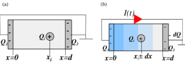
(a) (b) - - - Q i+ Q 1 Q 2 - - - - x=0 xi x=d - - - Q i + Q 1 Q 2 - - - x=0 xi±dx x=d I(t) -dQFig. 1. Principle of a stimulus method (example for a sample in short-circuit). The presence of a space charge
Qi induces influence charges Q1 and Q2 at electrodes (a).
When the sample equilibrium is perturbed by an external stimulus, charge variation at electrodes (Q2-dQ and Q1+dQ, respectively) occurs to restore it. Thus, the
transport of charge dQ from an electrode toward the other through the external circuit results in a current response I(t) =–dQ/dt.
Thermal methods use thermal diffusion as
the perturbation [3]. The sample is subjected to
a low variation of temperature on one of its
faces. The diffusion of heat through the
insulator expands the material in a non-uniform
manner, which slightly displaces the charges.
Additionally, the dielectric constant of the
material varies locally. Both processes induce
an electrical response, either a current between
the electrodes in short-circuit conditions or a
voltage in open-circuit conditions. That is
illustrated in Fig. 2. Different techniques have
been developed in order to generate heat
diffusion of various time dependences. When
pulsed lasers are used, the method is referred to
as the thermal pulse technique [4-6]. When
modulated lasers are used, the method is
Fig. 1. Principle of a stimulus method (example for a sample in short-circuit). The presence of a space charge Qiinduces influence charges Q1 and Q2
at electrodes (a). When the sample equilibrium is perturbed by an external stimulus, charge variation at electrodes (Q2−dQ and Q1+dQ, respectively)
occurs to restore it. Thus, the transport of charge dQ from an electrode toward the other through the external circuit results in a current response I(t) = dQ/dt.
or as a probe. All methods are based on the non-homogeneous perturbation of the electrostatic state of the structure under test by an external stimulus. For that purpose, adjacent electrodes are necessary. The tested material (or insulating structure) with its adjacent electrodes is referred herein to as the sample.
The idea lying behind the non-destructive space charge measurement methods is to provoke, with the aid of an external stimulus, a relative displacement of the space charges with respect to the electrodes, and/or a non-homogeneous variation of the permittivity. Indeed, in the absence of the stimulus, on both electrodes of the sample containing a space charge Qi,
influence charges (called Q1 and Q2 in Fig. 1) appear owing
to the total influence principle. During the application of the stimulus, these influence charges are modified by dQ, resulting in a transient current in the external circuit (if the sample is in short-circuit, as in the figure), or in a transitory modification of the voltage across the sample, if this latter is in open circuit. Thermal methods use thermal diffusion as the perturbation [3]. The sample is subjected to a low variation of temperature on one of its faces. The diffusion of heat through the insulator expands the material in a non-uniform manner, which slightly displaces the charges. Additionally, the dielectric constant of the material varies locally. Both processes induce an electrical response, either a current between the electrodes in short-circuit conditions or a voltage in open-short-circuit conditions. That is illustrated in Fig. 2. Different techniques have been devel-oped in order to generate heat diffusion of various time depen-dences. When pulsed lasers are used, the method is referred to as the thermal pulse technique [4]–[6]. When modulated lasers are used, the method is referred to as the laser-intensity-modulation-method (LIMM) [7], [8]. When alternative thermal waves are used, the method is known as alternative thermal wave method (ATWM) [18]. When temperature steps are used, the method is referred to as the thermal step method (TSM) [9]–[11]. The measured signal is the time derivative of the quantity of influence charges on the electrodes during the diffusion of the thermal wave. Whatever the thermal stimulus, the expression for the electric current is of the form [12]:
i(t) = −C Z ∞
0
α(x)E(x)∂∆T (x, t)
∂t dx (1)
where C is the fraction of the sample capacitance correspond-ing to the heated or cooled area, E the electric field distribution across the sample, α the equivalent linear expansion coefficient
Fig. 2. Principle of thermal methods: (a) Typical set-up: heat diffuses in the sample and slowly displaces the charges. The redistribution of influence charges at electrodes induces in turn an electrical current. (b) Typical signal: with a heat pulse, the amplitude of the signal is proportional to the interface electric field.
Fig. 3. Principle of pressure-wave-propagation methods: (a) Typical set-up: a pressure wave propagates in the sample and displaces the charges, which induce in turn an electrical current. (b) Typical signal: with a pressure pulse, the signal is an image of the charge distribution; time and position are related through the speed of sound.
which takes into account pyroelectricity, and ∆T is the im-posed temperature variation across the sample at every instant. Though the limits of the integral have been extended towards infinity, the electric field has a non-zero value only inside the sample, so the real limits are 0 and d, i.e. the sample limits. As charge density is related to electric field via Poisson’s equation ρ(x) = εdE/dx, obtaining the field distribution from Eq. (1) leads to the charge density distribution. Though the thermal methods have been firstly used to simply characterize the polarization homogeneity of pyroelectric films [3], they are now used in a wide variety of applications and thicknesses and many studies have been devoted to estimate the field and charge distributions from the signal [13]–[15], [19].
In the second family (acoustic methods), the pressure-wave-propagation (PWP) methods use elastic wave pressure-wave-propagation as the perturbation [20]. An elastic wave is transmitted into the sample. As the wave propagates through the insulator at the ve-locity of sound, it moves successively the encountered charges. That induces an electrical response which is measurable at the electrodes. This is illustrated in Fig. 3.
One advantage of using an elastic wave is that the short-circuit signal is an image of the charge distribution when using a pressure pulse: the time in the signal is simply the position in the sample divided by sound velocity. Different techniques have been developed in order to generate elas-tic waves by using shock tubes [21], lasers or piezoelec-tric materials. When lasers are used [22], [23], the method is referred to as the LIPP method (laser-induced-pressure-pulse). When a piezoelectric transducer generates the pres-sure wave [24], the method is referred to as the PIPS or the PIPWP methods (piezoelectrically-induced-pressure-step or piezoelectrically-induced-pressure-wave-propagation). In short-circuit conditions, the measured signal has a similar expression as the one of the thermal methods (1), except that α is the equivalent compressibility taking into account the electrostrictive effect and ∆T is replaced by the opposite of
Fig. 4. Principle of electro-acoustic methods: (a) Typical set-up: a voltage variation imposed to the sample changes the force acting on charges which generates in turn elastic waves that are measured by a transducer. (b) Typical signal: with a voltage pulse, the signal is an image of the charge distribution. Time and position are connected through the speed of sound.
the pressure (−P ).
The electro-acoustic methods use a fast varying electric stress as the perturbation [25]. The sample is subjected to a fast variation of the voltage applied to its electrodes. This produces a variation of the electrostatic force acting on each charge and thus creates elastic waves propagating from the charges and proportional to their values. These waves travel across the insulator at the speed of sound and can be measured by a transducer (Fig. 4). The measured signal is an image of the charge distribution since elastic waves arrive at a time depending on the distance between the charges and the transducer (the farther the charge, the later the signal). The electro-acoustic method is very similar to the pressure-wave-propagation method, cause and effect just being exchanged. When electrical pulses are applied [25]–[27], the technique is referred to as the PEA method (pulsed-electro-acoustic). When electrical steps are applied [28], the technique is referred to as the SEA method (step-electro-acoustic). The signal obtained with the PEA method is also similar to the one in the thermal methods. The stimulus ∆T is replaced by the pressure waves generated by the charges, these pressure waves having the shape of the electric stimulus. A second contribution to the signal proportional to the square of the electric stimulus exists however, but it can be often neglected or subtracted otherwise.
The above principles hold for any insulating structure, i.e. homogeneous (single-layer) and isotropic samples can be characterized as well as any insulating structure with physical properties varying with the depth-coordinate (mul-tilayers, materials under thermal or field gradient, etc.) If we take the case of a thermal method for an example, Eq. (1) shows that the measured signal is proportional to the overall capacitance of the sample and to the integral of the field multiplied by the α coefficient, which can vary with the depth coordinate with respect to the nature of the different layers composing the structure. Thus, this kind of techniques is fully applicable to multilayer insulating structures or to electronic structures as metal-insulator-semiconductor (MIS) capacitors [16], [17]. Acoustic techniques are also applicable to multi-materials, provided that the reflections of acoustic waves at the interfaces between different materials are taken into account properly [29]. On a larger scale, the presented principles can be used in symmetrical geometry, particularly in coaxial configurations, allowing the stimuli methods to be used on cables and axisymmetric components in general. Finally, the
Fig. 5. Evolution of the electric field distribution in a semiconduc-tor/XLPE/semiconductor sample during submission to a 10 kV/mm dc field at 25◦C for 15 minutes. Distortion and local enhancement of electric field is observed as a result of charge injection. Data obtained in voltage-on conditions by PEA [30].
use of adapted setups may allow performing 2D or 3D charge mappings. The possibilities offered today by these techniques are illustrated in the next section.
III. APPLICATIONS AND FEATURES OF STIMULI TECHNIQUES
A. Flat insulating samples
A large panel of experimental setups on insulating plaques and films has been proposed during the last decade, allow-ing multiple types of applications through measurements in voltage-on or voltage-off conditions. Some of the most typical ones are presented.
A widespread application of stimuli charge measurement methods is the survey of electric field distribution and space charge build-up in insulating samples submitted to electrical and thermal stress. This is particularly useful for material characterization, material design, process optimization and ageing assessment.
Fig. 5 above shows results obtained by the PEA method on a sandwich composed of an insulating layer (cross-linked polyethylene, XLPE) and two adjacent semiconducting elec-trodes, submitted to a dc field during several minutes. The figure provides an insight of the field enhancement and distor-tion caused by charge injecdistor-tion and accumuladistor-tion which may occur when a dielectric is submitted to a moderate to high dc stress.
Fig. 6 presents space charge distributions obtained by TSM in short-circuit conditions after a long-time submission of semicon-coated XLPE samples to a high ac field, at different temperatures. The effect of the temperature on space charge accumulation in deep traps is put into evidence. Formation of space charge zones at electrodes and in the bulk is shown. In the meantime, the data show that the charge amount does not increase monotonically with temperature (the highest charge accumulation is observed when stressing at 60◦C, not at 90◦C), bringing into focus that the accumulated charge results from the competition between injection at electrodes and conduc-tion, with specific field and temperature dependencies. On the other hand, a low but non nil charge amount is observed in the
Fig. 6. Space charge distribution in XLPE samples after submission to a 40 kV/mm dc field at 45◦C, 60◦C and 90◦C for 14 days. The presence of a low amount of space charge even without a previous submission to an electric field is shown (virgin sample). Temperature effect on charge accumulation in deep traps (injection/conduction competition) is evidenced. Measurements made in short-circuit by TSM [30].
virgin sample, putting into evidence that some space charge can be present in a material even without previous submission to an electric field, depending on the manufacturing process [31].
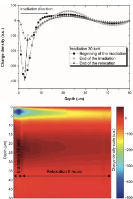
The effects of irradiation on insulating films can also be monitored with stimuli techniques [32]–[34]. Such data are useful when testing and studying materials for space applica-tions. Thus, Fig. 7 shows the charge and field distributions obtained by LIMM in a 50 µm gold-coated PTFE sample irradiated with an electron beam. The accumulation of charge near the sample surface during irradiation and its spreading and evacuation after stopping the irradiation can be observed.
Adapted experimental set-ups can allow obtaining 2D and 3D charge or polarization mapping in thin films [15], [35]– [38]. The study of electrets is a typical application. An exam-ple is shown in Fig. 8, where TPM and FLIMM have been used to carry out mapping of three-dimensional polarization in a 12 µm-thick PVDF films with the aid of a focused laser mounted on a controlled X-Y translation stage. It is shown in particular that even for such thin samples, inhomogeneities in the polarization can be encountered.
B. Coaxial configuration (cables)
As previously asserted, the principles of the stimuli methods can be used in any geometry, particularly in coaxial configura-tions, which make them suitable for measurements on power cables. This is of interest for assessing real cable insulation. For the developing sector of HVDC, space charge measure-ments in cable-like configurations are of significant impor-tance, as the different manufacturing process with respect to flat samples and the existence of a temperature gradient in the insulation of a power cable triggers phenomena that cannot be properly investigated otherwise. Consequently, PEA and TSM-based techniques allowing space charge measurements in cable-like configurations have been proposed.
Fig. 7. Electric field and space charge distributions in a thin PTFE sample irradiated with an electron beam of 30 keV. Charge accumulation and relaxation are shown. Measurements made in short-circuit conditions by LIMM [32].
Fig. 9 presents a typical PEA implementation. Variants exist in which the pulse voltage is applied to the conductor at cable end [39]. In the presented example, the measurement cell uses capacitive coupling to apply voltage pulses (dozens of ns, several kV, 400 Hz to 10 kHz) through the outer screen of the cable. HVDC voltages up to several hundreds of kV can be applied on the conductor using dedicated setups [40]. In order to apply a thermal gradient between the cable core and the outer screen, a cable loop heated by a heating trans-former is used, allowing measurements under thermal gradient. Examples of space charge profiles measured in a medium voltage cable in voltage-on and voltage-off conditions under temperature gradient are given in Fig. 10. They have been acquired while applying during 90 minutes a 60 kV voltage on the cable core (electric field of 18 kV/mm near the core and of 10 kV/mm near the outer screen), under a temperature gradient of 20◦C (70◦C on the core and 50◦C on the outer screen). The figure allows putting into evidence negative charge build-up occurring in the bulk of the insulation. The method was also applied to probe multilayer insulations in coaxial geometry.
A TSM implementation for power cables is shown in Fig. 11. It allows applying up to 500 kV dc to insulating thicknesses up to 25 mm, under temperature gradients obtained using heating transformers inserted in the cable loop. Two cables are used during the experiments: the studied cable and a second cable, which has the role to compensate the polarization and conduction currents during the space charge measurement.
The TSM measurement cell includes a coaxial thermal diffuser, where the thermal step is created on the outer semicon of the measured cable by the sharp arrival of a cold liquid
Fig. 8. Polarization maps at different depths z with respect to the surface in 12 µm-thick poly (vinylidene fluoride-trifluoroethylene)) (PVDF-TrFE (65%–35%)) films poled at 70 kV/mm. Measurements made in short-circuit conditions by TPM (top) and FLIMM (bottom) [38].
(Fig. 12). The measurement instrument is connected to the compensation cable, which is in series with the measured one during the space charge test. Field and charge profiles, measured in a long-term aged HVDC cable prototype (2600 h) under a temperature gradient of 14◦C (80◦C on the core, 66◦C on the outer semicon) and a voltage of -150 kV (43 kV/mm near the core), are presented in Fig. 13. They show a maximum field distortion after 15 days (up to 80 kV/mm), followed by a smoothing of the electric field distribution up to 105 days under stress. Field distribution may tend toward the purely resistive distribution, but this is far from being obvious even after 105 days testing. Double charge injection at contacts
Fig. 9. Diagram of a PEA measurement cell set up for space charge measurements on power cables [30].
Fig. 10. Space charge measurements by PEA in a medium voltage cable submitted to dc stress (-60 kV) under temperature gradient (70/50◦C) [41].
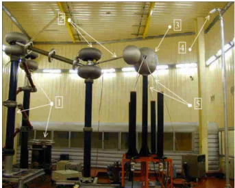
Fig. 11. TSM setup for space charge measurements in HVDC cables. 1: HVDC Supply; 2: Voltage divider and HV switch; 3: cables junction sphere; 4: HV monitoring device (field mill); 5: Cable under test and compensation cable fitted with oil-filled lab terminals [42].
seems to prevail during the ageing campaign, even if negative charge build-up is fading whereas positive charges are pro-gressing toward the bulk of the insulation. Thus, as a key result of this investigation, maximum field distortions and space charge levels are observed after 10–15 days ageing. Beyond
Fig. 12. Thermal diffuser (400 mm long) used to generate the thermal step from the outer screen of a cable [42].
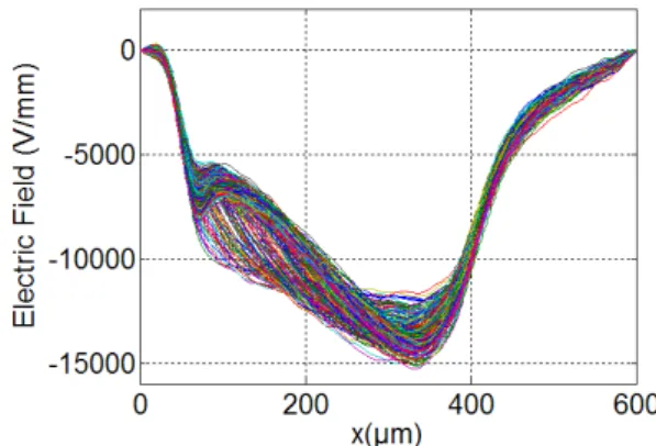
Fig. 13. Electric field distributions obtained by TSM in a cable during long-time dc conditioning under thermal gradient. Capacitive and resistive (steady state) distributions included for comparison [42].
this duration, the distortions are getting weaker, as negative charges start to be evacuated or recombined and positive ones are building up.
It must be underlined that information such as that illus-trated in the above examples constitutes a significant input for insulation design and assessment of the behavior of HVDC equipment, which requires a high degree of reliability, and can be obtained only by direct measurement with stimuli methods.
C. Microelectronic structures
If we take the case of a thermal method for an example, Eq. (1) shows that the measured signal is proportional to the overall capacitance of the sample and to the integral of the field multiplied by the α coefficient, which can vary with the depth coordinate with respect to the nature of the different layers composing the structure. Thus, the technique is fully applicable to electronic structures as metal-insulator-semiconductor (MIS) capacitors. In the case of a metal-oxide-semiconductor (MOS) structure for which the composition is shown in Fig. 14, the measured signal i(t) will carry information about the position and the amount of charges contained in the insulating oxide, in the semiconductor and at the interface between the two materials.
Typical dimensions of MOS structures are of the order of nanometers to microns for the oxide and of several hundreds of microns for the doped semiconducting layer (substrate). In order to study phenomena related to reliability and ageing of such components and for designing new structures, it is important to be able to locate as precisely as possible the elec-tric charges within the oxide and at the oxide/semiconductor interface. Indeed, the charges accumulated in the insulating
8
the field multiplied by the α coefficient, which
can vary with the depth coordinate with respect
to the nature of the different layers composing
the structure. Thus, the technique is fully
applicable to electronic structures as
metal-insulator-semiconductor (MIS) capacitors. In
the case of a metal-oxide-semiconductor (MOS)
structure for which the composition is shown in
Fig. 14, the measured signal i(t) will carry
information about the position and the amount
of charges contained in the insulating oxide, in
the semiconductor and at the interface between
the two materials.
ΔT0>0 T CSi Bias voltage Vg Vox SiO2 Al Cox CSi Si-SiO2 interface Cox αSi αox Vs Vs Si I(t) I(t) pA pA Charged Si
Fig. 14. Thermal method applied to a metal-oxide-
semiconductor (MOS) structure. The measured signal is
the derivative of the influence charge with time,
providing information on the oxide and semiconductor
charge [16-17].
Typical dimensions of MOS structures are
of the order of nanometers to microns for the
oxide and of several hundreds of microns for
the doped semiconducting layer (substrate). In
order to study phenomena related to reliability
and ageing of such components and for
designing new structures, it is important to be
able to locate as precisely as possible the
electric charges within the oxide and at the
oxide/semiconductor interface. Indeed, the
charges accumulated in the insulating layer and
at the interface may provoke malfunction of the
component even if the insulating layer does not
break down. The classical methods used in
micro-electronics are either destructive
(etch-off technique) or of insufficient spatial
resolution (only the charge close to the
substrate can be assessed by the
capacitance-voltage method). Determining the doping
profile in the semiconductor is also of interest
for improving manufacturing. In all these fields,
significant progress can be made through the
use of stimuli methods.
N-type Silicon Nd= 1015cm-3 Nd+= 1017cm-3 500µm 120nm 500nm 500nm Aluminum Aluminum 100-300nm SiO2 (oxide) Surface 0,19 cm2 Thermal SiO2 Thermal diffuser -5V >V > +5V Current amplifier pA I(t)
C
SiC
oxSpace charge zone in Si
Fig. 15. Experimental set up for thermal step
measurements on a MOS structure [16-17].
0s 1s 2s 3s 4s 5s 6s 7s 8s 9s 10s -60pA -40pA -20pA 0A 20pA 40pA 60pA -1V, T0h -3V, T0h -5V, T0h 0.5V, T0h -0.5V, T0h 1V, T0h 3V, T0h 5V, T0h T her m al S tep C ur rent Time
Fig. 16. Typical TSM signals measured for different
voltages V
gapplied to a MOS sample [16].
Interesting information on the charge within
such a structure can be obtained relatively
easily by using a low thermal stimulus of
several degrees [16-17]. Fig. 15 shows such a
setup where a thermal stimulus is applied with
the aid of a liquid circulating in a radiator in
contact with the measured sample (TSM). The
signals measured for different voltages applied
to the structure V
gare shown in Fig. 16: it can
be seen that a characteristic signal is obtained
for a given voltage, as the semiconductor is
driven into accumulation, depletion or
inversion regime. The I(V
g)|
Maxdata can be
plotted to obtain a characteristic of the structure
(Fig. 17), then by combining it with low
frequency capacitance-voltage measurements
one can obtain the total charge of structure and
the charge characteristics to the oxide and the
interface (Fig. 18).
Complete components, like trench-gated
IGBT can be characterized in such ways in
order to assess the evolution of the electrical
Fig. 14. Thermal method applied to a metal-oxide- semiconductor (MOS) structure. The measured signal is the derivative of the influence charge with time, providing information on the oxide and semiconductor charge [16], [17].
Fig. 15. Experimental set up for thermal step measurements on a MOS structure [16], [17].
layer and at the interface may provoke malfunction of the component even if the insulating layer does not break down. The classical methods used in micro-electronics are either destructive (etch-off technique) or of insufficient spatial reso-lution (only the charge close to the substrate can be assessed by the capacitance-voltage method). Determining the doping profile in the semiconductor is also of interest for improving manufacturing. In all these fields, significant progress can be made through the use of stimuli methods.
Interesting information on the charge within such a structure can be obtained relatively easily by using a low thermal stimulus of several degrees [16], [17]. Fig. 15 shows such a setup where a thermal stimulus is applied with the aid of a liquid circulating in a radiator in contact with the measured sample (TSM). The signals measured for different voltages applied to the structure Vg are shown in Fig. 16: it can
be seen that a characteristic signal is obtained for a given voltage, as the semiconductor is driven into accumulation, depletion or inversion regime. The I(Vg)|Max data can be
plotted to obtain a characteristic of the structure (Fig. 17), then by combining it with low frequency capacitance-voltage measurements one can obtain the total charge of structure and the charge characteristics to the oxide and the interface (Fig. 18).
Complete components, like trench-gated IGBT, can be char-acterized in such ways in order to assess the evolution of the
Fig. 16. Typical TSM signals measured for different voltages Vg applied to
a MOS sample [16].
Fig. 17. Maximum of the measured thermal step currents IM axfrom Fig.
16 plotted versus the gate voltage Vg.
electrical state of the oxide [43]. It is worth to mention that, in general, the sensitivity of the thermal methods is at least one order of magnitude above that of the capacitance-voltage method, thus allowing putting into evidence changes into the electrical state of the insulators that cannot be observed otherwise [17], [44].
To reduce side effects, the heat flux must be concentrated as much as possible in the gate area. One way to achieve this is to provoke the thermal perturbation by a non-contact method, for instance by using a laser pulse, i.e. using the TPM. This also presents the advantage of diminishing the thermal inertia of the system, thus allowing tending toward much higher resolutions. An example of such a measurement made on a MIS structure composed of 300 nm-thick Si3N4 coated on a 1018 cm−3
p-Fig. 18. Total charge of the MOS structure (Q0) and oxide + interface charge
(Q0− QS) versus substrate potential VS.
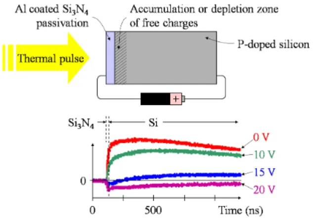
Fig. 19. TPM applied to a metal- insulator- semiconductor (MIS) structure and transient voltage signals measured for different voltages applied to the sample [45].
doped Si substrate is shown in Fig. 19. The thermal stimulus was generated with 0.4 mJ – 50 ps laser pulses. In this case, the acquired signal contains more information on the electric field distribution across the oxide and the substrate, as the sampling period is much closer to the transit times of the thermal wave across the two layers: provided that the temperature diffusion through the sample is accurately known, such measurement can allow to closely approach the electric field distribution in the sample.
PWP methods can also be used to study microelectronic components as Schottky diodes, PN diodes and MIS struc-tures. Similarly to the thermal methods, the spatial resolution obtained with the setups used is presently not sufficient to resolve the fine structure of the charge distribution at an interface. The whole charge quantity is determined instead but that already brings more information than the capacitance-voltage measurement technique. An example of measurements carried out with the same structure as the one of Fig. 19, except that the pressure wave is transmitted from the Schottky side
Fig. 20. LIPP method applied to a MIS structure and transient voltage signals measured for different voltages applied to the sample [46].
Fig. 21. Amplitude of the MIS interface peak as the function of the applied voltage [47].
of the sample as illustrated in Fig. 20, is given in the latter. The PWP signal presents two clear peaks, the first being the signature of the Schottky interface and the second the one of the MIS interface. Discerning the two interfaces is already a great improvement compared to the capacitance-voltage technique. With the applied capacitance-voltage variation, charge variation occurs mainly at the MIS interface. Plotting the amplitude of the second peak as a function of applied voltage leads to similar results than the one found with the thermal methods (Fig. 21), as shown in Fig. 14. Note however that the voltage is applied in the opposite way in the two figures.
The above examples put into evidence that measurement methods usually implemented for thicker materials give in-teresting new information in the case of electronic structures. However, mainly the overall charge quantity could be accessed so far with such methods, and the details of the distributions remain elusive. Full access to the charge and field repartitions requires an increase in the resolutions, which is one of the challenges to be overcome in the near future.
D. Synthesis of the features of the stimuli methods
Although the described families of methods are similar in the information they can provide [2], their implementation is complementary. Consequently, choosing one of them for a particular application depends on the targeted thickness, the targeted resolution, the acceptable duration of the measure-ment and of the signal-to-noise ratio, as well as on the degree of sophistication of the needed equipment.
Thus, thermal methods provide high sensitivity and a good spatial resolution close to interfaces without requiring wide bandwidth measuring systems. However, far from the inter-faces the spatial resolution decreases owing to the physics of thermal diffusion. Methods as LIMM and TPM are well-suited for thin samples (dozens of microns and below), where they can provide resolutions of the order of the micron near the electrode where the thermal stimulus is applied, but the low amount of heat available limits their use for thicker samples. The TSM can be used on much higher thicknesses, as there is theoretically an infinite amount of energy available from the stimulus. The TPM is a fast method (the signal duration is of the order of the µs), while TSM signals last from several µs to several minutes and LIMM characterization requires durations of the order of several dozens of minutes.
Pressure-wave-propagation and electro-acoustic methods give a similar spatial resolution throughout the thickness, but require wide bandwidth measuring system and their sensi-tivities are usually one order of magnitude lower than for the thermal methods. In turn, their fast response (µs) allows analysis of rapidly varying phenomena. Thermal and pressure-wave-propagation methods have good signal to noise ratios, and therefore can be used for thick samples (e.g., up to 30 mm and above for the TSM). Electro-acoustic methods provide a better decoupling between signal and electric stress and therefore can be safely used under fields close to electrical breakdown situations.
IV. RECENT ACHIEVEMENTS AND CHALLENGES
There is today a growing interest in setting up techniques able to supply high and very high spatial resolutions, especially in view of closely studying interface phenomena and very thin structures. The best resolutions achievable at the present time are of the order of 1 µm for the thermal methods and of 5 to 10 µm for the acoustic methods. Obtaining higher spatial resolutions requires a significant increase of the bandwidth of both the perturbation and the detection set-up. Indeed, spatial resolution is closely related to bandwidth since time and space are connected through diffusion or propagation process [48]. It must also be kept in mind that, whatever the method, the resolution increases with the decrease of the thickness and the increase of the stimulus magnitude. Thus, submicronic resolutions can be reachable only on very thin samples (< 50 µm). However, increasing the resolution in thicker structures (> 100 µm) is also of interest, as the homogeneity degree of such structures is generally higher than 1 µm due to the manufacturing process.
Though the noise level should be taken into account to determine the reachable spatial resolution, the direct resolution is roughly given by (Dt)1/2 in the case of thermal methods (D is the thermal diffusivity of the sample and t is the time) and by vst in the case of electro-acoustic methods (vs is the
sound velocity). In the case of the thermal methods, (Dt)1/2 represents the position for which the temperature variation is half the one at the interface. D is of the order of 10−7 m2/s in polymeric materials and of the order of 10−6 m2/s in silicon dioxide. Therefore, a resolution below 100 nm in
Fig. 22. Principle of thermal methods with femtosecond laser pulses. A pump beam perturbs the sample. The induced charge displacement generates an electromagnetic wave which is measured by electro-optic (EO) sampling. A delay stage provides the time sweep.
organic layers and components requires a bandwidth higher than 10 MHz, whilst the bandwidth needed for oxides is of the order of 0.1 to 10 GHz. In the first case, nanosecond thermal pulses are required, while femtosecond pulses are needed in the second case. Conventional heaters or pulse generators are no longer adapted and the bandwidth of the usual measuring instruments is not sufficient. New kinds of implementation are required.
Tests where the thermal perturbation is produced by a femtosecond laser pulse in a thin sample have been carried out [49]. When charges are perturbed by heat or by the elastic waves, they emit an electromagnetic wave which can be measured by electro-optic sampling (Fig. 22). Though a spatial resolution better than 50 nm in silicon dioxide could be expected, which is equivalent to 22 nm in polymeric materials, the signal to noise ratio is very poor and obtaining convincing results is still a long way to go with all optical instrumentation.
The technology for obtaining spatial resolutions below 100 nm is therefore at reach, although requiring dedicated equipment such as wide bandwidth acousto-optic modulators for heat excitation. Though most of the needed instruments are now available, reaching the proposed goal remains a challenge, as several experimental and theoretical problems must be solved.
First of all, the perturbation needs to be correctly applied and the signal must be detected above the noise. Measuring the signal is however not sufficient to accurately estimate the charge distribution with the thermal method. Indeed, results drastically depend on the boundary conditions applied in the deconvolution calculations. The simultaneous measurement of the signal and of the interface temperature is of great help, as it allows accessing directly to the stimulus and thus increases the calculation precision for temperature distribution across the material. The feasibility of bolometric measurements from the heated electrode have already been demonstrated [50], but care must be paid to the experimental set up, in particular to the terminals for limiting additional load capacitance and noise increase (Fig. 23).
As the thermal “wave” applied to the electrode attenuates while it diffuses toward the sample bulk, the resolution de-creases with the distance from the thermally excited electrode. To increase the bulk resolution, it is then necessary to increase the amount of heat transferred to the sample. For analyzing thicker samples, or if thick electrodes are used (e.g., semicon electrodes), the use of a temperature step is preferable, as the amount of heat supplied to the sample is then virtually infinite.
Fig. 23. Experimental set-up proposed for very high resolution thermal method with heat pulse technique [49]. The sample is under voltage and the surface temperature is measured by bolometry. For that purpose, a continuous current flows through the heated electrode and the voltage appearing is measured.
This can be achieved with a fluid at a given temperature. In this case, the challenge relies in optimizing the thermal transfer between the fluid and the sample in order to increase the measurement dynamics as much as possible. Recent studies have shown that resolutions of the order of 1 µm and below can be theoretically reached with such a setup in 100 µm-thick insulating samples provided with 30 µm-µm-thick semicon electrodes [51].
Whatever the form of the thermal stimulus, obtaining the precise amplitude of the thermal excitation by direct mea-surements is not really useful, since calibration procedures can be used to scale the signal amplitude [11]; only the time evolution of the temperature is required in order to perform the mathematical deconvolution of the Eq. (1), which is a Fredholm equation of the first kind. However, a problem which must be addressed is the improvement of the temperature matrix conditioning, either by mathematical techniques or by the adaptation of the thermal stimulus (boundary conditions), allowing to obtain a less ill-posed inverse problem. A sig-nificant work concerning thermal and signal analysis must therefore be performed for improving signal deconvolution.
In the case of the acoustic methods, the resolution is deter-mined by the stimulus width, and for the PEA, by the thickness of the acoustic actuator [52]–[54]. The classical PEA appara-tus, with a 5 ns-short duration pulse and a Poly(vinylidene fluoride)–PVDF–piezoelectric sensor of 9 µm-thick, allows electrical characterization of the order of 200 to 500 µm-thick dielectric materials by measuring the spatial and temporal evo-lution of internal charge distributions with a spatial resoevo-lution of about 10 µm. In order to improve the spatial resolution, it is necessary to reduce the piezoelectric sensor thickness and the pulse duration. According to the discerning resolution criterion [55], two planes of charges can be distinguished when they are spaced by a minimum distance of 2.1 µm when using a 1 µm thick piezoelectric sensor and a ns-short duration pulse.
Increasing the spatial resolution requires a bandwidth in-crease as formerly shown. Since the velocity of sound is about 2000 m/s in polymeric materials, obtaining resolutions as high as 100 nm requires a 10 GHz bandwidth. Until now, pressure-wave-propagation and pulsed-electro-acoustic methods have been implemented with wide bandwidth stimuli such as pulses. But for a 10 GHz bandwidth, the power required to generate a significant signal is too important. The overcome is to use continuous wave stimuli at different frequencies. One great advantage of such stimuli is that electrical matching can be used to drastically improve the coupling coefficient and thus
Fig. 24. Experimental set-up proposed for very high resolution pulsed-electro-acoustic or pressure-wave-propagation methods. Matching circuits at the generation and measurement sides are used to optimize the power transfer and thus the signal to noise ratio.
the signal level.
Such a scheme is presented in Fig. 24 in the case of the pulsed-electro-acoustic method or, one should say, the modulated-electro-acoustic method. A generator produces a continuous electric wave at a given frequency which passes through a matching circuit in order to optimize the energy transfer to the sample. Elastic waves generated by the charges travel through the sample and a wave-guide to reach a high frequency transducer. Here again, a matching circuit is used to measure the signal response with an improved signal to noise ratio. The procedure is repeated at various frequencies from 100 MHz to 10 GHz in order to reconstruct the space charge distribution signal from its spectrum. The same scheme can be used for the pressure-wave-propagation method by simply using the generator at the transducer side and the sample at the measurement side.
In these schemes however, coupling is a key parameter since it is necessary to transmit very short duration elastic waves from one material to another. Since it is admitted that an interface is transparent if its thickness is smaller than 1/20 of the smallest wavelength, the interface needs to be roughly better than 5 nm to reach 100 nm spatial resolution. Moreover, the elastic wave must not diffuse on any impurity once transmitted into the material. This requires, in addition, that the used material must be sufficiently pure, such as crystals. A work around can be a measurement of the electro-mechanical conversion energy when the stimulus is applied as recently proposed [56]. In that case, the response of the material is measured from the energy of the stimulus which is not converted. This simplifies the material couplings and the measuring setup, but requires to uncouple a small signal from a large one.
On another level, the increasing interest for HVDC trans-missions led to a demand of on-site space charge measurement installations, able to be used in voltage-on conditions directly on components with thick insulating layers like HVDC cables. The challenges encountered in this field are related mainly to the attenuation of the stimulus in very thick samples and to the influence of the HVDC environment. Recent work reported PEA and TSM implementations able to be used on full-size HVDC cables with insulating thicknesses up to 30 mm [57], [58]. This kind of space charge probes are now being used during HVDC cable prequalification ageing tests (Fig. 25) and could be key tools in the development of future extra high voltage transmission apparatus (up to 800 kV).
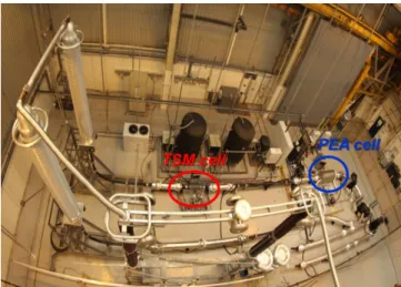
Fig. 25. Full-size HVDC cable loop set up for a prequalification ageing programme, including TSM and PEA cells for space charge measurements [57].
Finally, one interesting way to explore using the direct stimuli space charge measurement techniques is the domain of dielectric liquids. Thus, when a liquid dielectric is put into contact with a solid wall, an electrical double layer (EDL) containing charges of opposite sign appear at the solid/liquid interface. Many studies have been made to measure the EDL charge, but its theoretical distribution has not been confirmed experimentally yet, as so far there has been no method allow-ing direct measurement of space charge profiles in dielectric liquids. This is where direct space charge measurement meth-ods can bring significant information. Latest developments have demonstrated the feasibility of using a thermal stimulus to analyze the solid/dielectric interface field [59]. Although further developments are still to be made both at the theoretical and experimental level, the obtained results are encouraging in the perspective of new fallouts for stimuli methods.
V. CONCLUSIONS AND PROSPECTS
Lying on the principle of using low external stimuli to perturb the equilibrium of insulating samples or structures, the direct, non-destructive space charge measurement techniques have been continuously developed for the last three decades to determine and monitor electric field and charge distributions in a wide panel of solid dielectrics of various thicknesses submit-ted to multiple types of stress (electrical, thermal, radiative). Their use is now being extended to microelectronic structures, full-size components for electric power transmission and liquid dielectrics.
High resolutions down to the submicronic level are now at reach. They will hopefully allow in the next decade to study very thin samples, solid/solid and solid/liquid interfaces. This will undoubtedly contribute to increase the understanding and control of the physical mechanisms which govern charge transport and trapping, and open the way to new applications in the domain of electrical engineering and electronics.
REFERENCES
[1] Y. Zhang, J. Lewiner, C. Alqui´e, and N. Hampton, “Evidence of strong correlation between space-charge buildup and breakdown in cable
“Analysis of response of pyroelectric optical detectors,” Journal of Applied Physics, vol. 45, pp. 3296–3303, 1974.
[4] R. E. Collins, “Analysis of spatial distribution of charges and dipoles in electrets by a transient heating technique,” Journal of Applied Physics, vol. 47, pp. 4804–4808, 1976.
[5] R. E. Collins, “Practical application of the thermal pulsing technique to the study of electrets,” Journal of Applied Physics, vol. 51, pp. 2973–2986, 1980.
[6] F. I. Mopsik and A. S. Dereggi, “Numerical evaluation of the dielectric polarization distribution from thermal-pulse data,” Journal of Applied Physics, vol. 53, pp. 4333–4339, 1982.
[7] S. B. Lang and D. K. Das-Gupta, “Laser-intensity-modulation method: A technique for determination of spatial distributions of polarization and space charge in polymer electrets,” Journal of Applied Physics, vol. 59, pp. 2151–2160, 1986.
[8] J. L. Franceschi and V. Haas, “Laser thermoacoustic modulation for space charge measurement,” Applied Physics Letters, vol. 70, pp. 2236–2237, 1997.
[9] A. Toureille and J. P. Reboul, “The thermal-step-technique applied to the study of charge decay in polyethylene thermoelectrets,” in 6th International Symposium on Electrets,(ISE 6) Proceedings., Sep 1988, pp. 23–27.
[10] S. Sakai, M. Ishida, M. Date, and T. Furukawa, “Changes in photo-induced pyroelectric transients during polarization reversal in VDF-TrFE copolymers,” in [1991 Proceedings] 7th International Symposium on Electrets (ISE 7), Sep 1991, pp. 472–476.
[11] P. Notingher, S. Agnel, and A. Toureille, “Thermal step method for space charge measurements under applied dc field,” IEEE Transactions on Dielectrics and Electrical Insulation, vol. 8, pp. 985–994, 2001. [12] A. Cernomorcenco and P. Notingher Jr., “Application of the thermal
step method to space charge measurements in inhomogeneous solid insulating structures: A theoretical approach,” Applied Physics Letters, vol. 93, p. 192903, 2008.
[13] A. Petre, D. Mary, and D. Marty-Dessus, “Electroluminescence and space charge measurements for the study of PEN ageing under UV irradiation,” Journal of Optoelectronics and Advanced Materials, vol. 6, pp. 1049–1054, 2004.
[14] A. Petre, D. Marty-Dessus, L. Berquez, and J.-L. Franceschi, “A comparison of different mathematical treatments for solving the inverse problem in focused laser intensity modulation method,” Japanese Journal of Applied Physics, Part 1: Regular Papers and Short Notes and Review Papers, vol. 43, pp. 2572–2579, 2004.
[15] A. Petre, D. Marty-Dessus, L. Berquez, and J. L. Franceschi, “Space charge cartography by FLIMM on sem-irradiated PTFE thin films,” Journal of Electrostatics, vol. 64, pp. 492–497, 2006.
[16] L. Boyer, O. Fruchier, P. Notingher, S. Agnel, A. Toureille, B. Rousset, and J. L. Sanchez, “Analysis of data obtained using the thermal-step method on a MOS structure: An electrostatic approach,” IEEE Transactions on Industry Applications, vol. 46, pp. 1144–1150, 2010. [17] L. Boyer, B. Rousset, P. Notingher Jr., S. Agnel, and J. L. Sanchez,
“Measurement of charge evolution in oxides of DC stressed MOS structures,” in 2010 IEEE Industry Applications Society Annual Meeting, Oct 2010, pp. 1–8.
[18] J. M. Reboul and F. Mady, “Space charge measurements by the alternating thermal wave method: thermal analysis and simulations for data processing improvement,” in Proceedings of the 2004 IEEE International Conference on Solid Dielectrics (ICSD), vol. 1, July 2004, pp. 256–259.
[19] P. Notingher, A. Toureille, S. Agnel, and J. Castellon, “Determination of electric field and space charge in the insulation of power cables with the thermal step method and a new mathematical processing,” IEEE Transactions on Industry Applications, vol. 45, pp. 67–74, Jan 2009. [20] P. Laurenc¸eau, G. Dreyfus, and J. Lewiner, “New principle for the
determination of potential distributions in dielectrics,” Physical Review Letters, vol. 38, pp. 46–49, 1977.
[21] P. Laurenc¸eau, J. Ball, G. Dreyfus, and J. Lewiner, “Une m´ethode nouvelle de d´etermination de la distribution spatiale des potentiels dans les di´electriques (in French),” Comptes rendus de l’Acad´emie des sciences, vol. 283, pp. 135–138, 1976.
and W. Eisenmenger, “Investigation of piezoelectricity distributions in poly(vinylidene fluoride) by means of quartz- or laser-generated pressure pulses,” Journal of Applied Physics, vol. 55, pp. 2769–2775, 1984.
[25] T. Maeno, H. Kushibe, T. Takada, and C. M. Cooke, “Pulsed electro-acoustic method for the measurement of volume charges in E-beam irradiated PMMA,” in Conference on Electrical Insulation Dielectric Phenomena - Annual Report 1985, Oct 1985, pp. 389–397.
[26] T. Takada, T. Maeno, and H. Kushibe, “An electric stress-pulse technique for the measurement of charges in a plastic plate irradiated by an electron beam,” IEEE Transactions on Electrical Insulation, vol. EI-22, pp. 497– 501, 1987.
[27] J. B. Bernstein, “Analysis of the electrically stimulated acoustic-wave method for observing space charge in semi-insulating films,” Physical Review B, vol. 44, pp. 10 804–10 814, 1991.
[28] E. Motyl, “Comparison between step and pulsed electroacoustic techniques using both PVDF and LiNbO3 transducers,” Journal of Electrostatics, vol. 51-52, pp. 530–537, 2001.
[29] R. Bodega, P. H. F. Morshuis, and J. J. Smit, “Space charge mea-surements on multi-dielectrics by means of the pulsed electroacoustic method,” IEEE Transactions on Dielectrics and Electrical Insulation, vol. 13, pp. 272–281, 2006.
[30] P. Notingher and G. Teyssedre, “Performance of the materials used in the development of HVDC cables,” presented at the European Seminar on materials for HVDC cables and accessories : Performance, Modeling, Testing, Qualification (Jicable HVDC’13), Perpignan, France, November 2013, pp. 776–779.
[31] A. Toureille, P. Notingher Jr., N. Vella, S. Malrieu, J. Castellon, and S. Agnel, “The thermal step technique: An advanced method for studying the properties and testing the quality of polymers,” Polymer International, vol. 46, pp. 81–92, 1998.
[32] S. Bouchareb, V. Griseri, and L. Berquez, “In situ space charge profile measurements on electronic irradiated material by LIMM,” in 2013 IEEE International Conference on Solid Dielectrics (ICSD), June 2013, pp. 776–779.
[33] X. T. Nguyen, S. Bouchareb, V. Griseri, and L. Berquez, “Post-electronic irradiation measurements by PEA and FLIMM methods on dielectric films,” in 2011 Annual Report Conference on Electrical Insulation and Dielectric Phenomena, Oct 2011, pp. 812–815.
[34] X. T. Nguyen, V. Griseri, and L. Berquez, “In-situ space charge measurements on dielectrics during electronic irradiation by PEA,” in 2013 Annual Report Conference on Electrical Insulation and Dielectric Phenomena, Oct 2013, pp. 226–269.
[35] D. Marty-Dessus, L. Berquez, A. Petre, and J. L. Franceschi, “Space charge cartography by FLIMM: A three-dimensional approach,” Journal of Physics D: Applied Physics, vol. 35, pp. 3249–3256, 2002. [36] A. Mellinger, R. Singh, and R. Gerhard-Multhaupt, “Fast thermal-pulse
measurements of space-charge distributions in electret polymers,” Review of Scientific Instruments, vol. 76, p. 013903, 2005.
[37] A. Mellinger, R. Singh, M. Wegener, W. Wirges, R. Gerhard-Multhaupt, and S. B. Lang, “Three-dimensional mapping of polarization profiles with thermal pulses,” Applied Physics Letters, vol. 86, p. 082903, 2005. [38] C. D. Pham, A. Petre, L. Berquez, R. Flores-Suarez, A. Mellinger, W. Wirges, and R. Gerhard, “3D high-resolution mapping of polarization profiles in thin poly(vinylidenefluoride-trifluoroethylene) (PVDF-TrFE) films using two thermal techniques,” IEEE Transactions on Dielectrics and Electrical Insulation, vol. 16, pp. 676–681, 2009.
[39] T. Takada, “Acoustic and optical methods for measuring electric charge distributions in dielectrics,” IEEE Transactions on Dielectrics and Elec-trical Insulation, vol. 6, pp. 519–547, 1999.
[40] N. Hozumi, H. Suzuki, T. Okamoto, K. Watanabe, and A. Watanabe, “Direct observation of time-dependent space charge profiles in XLPE cable under high electric fields,” IEEE Transactions on Dielectrics and Electrical Insulation, vol. 1, pp. 1068–1076, 1994.
[41] B. Vissouvanadin, “Mat´eriaux de cbles `a isolation synth´etique pour des applications au transport d’´energie HVDC (in french),” Ph.D. dissertation, University of Toulouse, 2013.
[42] J. Castellon, P. Notingher Jr., S. Agnel, A. Toureille, J. F. Brame, P. Mirebeau, and J. Matallana, “Electric field and space charge
measurements in thick power cable isulation,” IEEE Electrical Insulation Magazine, vol. 25, pp. 30–42, 2009.
[43] S. Baudon, “ ´Etude de l’influence des contraintes appliqu´ees sur l’´evolution des propri´et´es di´electriques des couches minces isolantes dans les composants semiconducteurs de puissance (in french),” Ph.D. dissertation, University of Montpellier, 2013.
[44] L. Boyer, “Analyse des propri´et´es de l’oxyde de grille des com-posants semi-conducteurs de puissance soumis `a des contraintes ´electrothermiques cycliques : vers la d´efinition de marqueurs de vieil-lissement (in french),” Ph.D. dissertation, University of Montpellier, 2010.
[45] S. Hol´e, T. Ditchi, and J. Lewiner, “Can non-destructive space charge measurement techniques have fallout in other fields?” in Proceedings of the 11th International Symposium on Electrets, October 2002, pp. 32–35.
[46] S. Hol´e and J. Lewiner, “Direct measurement of trapped and free charge distributions in semiconductors,” Applied Physics Letters, vol. 84, pp. 1308–1310, 2004.
[47] S. Hol´e, “Mesure des distributions de charges d’espace : des isolants aux structures `a semi-conducteurs (in french),” Habilitation Thesis, University of Paris 6, 2007.
[48] S. Hol´e, “Resolution of direct space charge distribution measurement methods,” IEEE Transactions on Dielectrics and Electrical Insulation, vol. 15, pp. 861–871, 2008.
[49] G. Dagher, S. Hol´e, and J. Lewiner, “A preliminary study of space charge distribution measurements at nanometer spatial resolution,” IEEE Transactions on Dielectrics and Electrical Insulation, vol. 13, pp. 1036– 1041, 2006.
[50] C. Filloy-Corbrion, C. Boue, E. G´eron, T. Ditchi, J. Lucas, S. Hol´e, P. Notingher, S. Agnel, D. Marty-Dessus, L. Berquez, and G. Teysse-dre, “Surface temperature measurement for space charge distribution measurements with thermal methods,” IEEE Transactions on Dielectrics and Electrical Insulation, vol. 22, pp. 1506–1511, 2015.
[51] S. Zhao, J. Laurentie, P. Notingher, J. Castellon, A. Allais, A. Combessis, G. Perego, and L. Boyer, “High resolution thermal step system for space charge measurements in materials for HVDC insulation: Design and setup,” in 2016 IEEE International Conference on Dielectrics (ICD), vol. 1, July 2016, pp. 231–234.
[52] M. Arnaout, L. Berquez, F. Baudoin, and D. Payan, “Contribution to improving the spatial resolution of a pulsed electro acoustic cell measurement: An analysis of acoustics waves propagation,” in 2010 10th IEEE International Conference on Solid Dielectrics, July 2010, pp. 1–4. [53] L. Galloy, L. Berquez, F. Baudoin, and D. Payan, “PSpice modeling of the acoustic detector for a pulsed electro-acoustic cell,” in 2013 IEEE International Conference on Solid Dielectrics (ICSD), June 2013, pp. 468–471.
[54] K. Kumaoka, T. Kato, H. Miyake, and Y. Tanaka, “Development of space charge measurement system with high positionalal resolution using pulsed electro acoustic method,” in Proceedings of 2014 International Symposium on Electrical Insulating Materials, June 2014, pp. 389–392. [55] S. Hol´e and J. Lewiner, “High-resolution multidimensional space charge measurement using elastic wave methods,” Physical Review B -Condensed Matter and Materials Physics, vol. 64, p. 104106, 2001. [56] L. Hamidouche, E. G´eron, T. Ditchi, and S. Hol´e, “High frequency
spectroscopy for high spatial resolution space charge measurements,” presented at the 15th International Symposium on Electrets (ISE), Baltimore, MD, August 2015, IX. 8.
[57] A. Tzimas, G. Lucas, K. J. Dyke, F. Perrot, L. Boyer, P. Mirebeau, S. Dodd, J. Castellon, and P. Notingher, “Space charge evolution in XLPE HVDC cable with thermal-step-method and pulse-electro-acoustic,” in Proceedings of European Seminar on materials for HVDC cables and accessories : Performance, Modeling, Testing, Qualification (Jicable ’15), Versailles, France, June 2015, A8.1.
[58] L. Boyer, P. Mirebeau, S. Girard, T. Garcia, M. Plopeanu, J. Castellon, P. Notingher, S. Agnel, A. Toureille, D. Jossien, and Y. Depuidt, “Development of an industrial space charge measurement facility for extruded HVDC full scale cables,” in European Seminar on materials for HVDC cables and accessories : Performance, Modeling, Testing, Qualification (Jicable ’15), Versailles, France, June 2015, A8.2. [59] J. C. Laurentie, T. Paillat, Y. Chnidir, A. Toureille, G. Touchard,
and P. Notingher, “Space charge measurement in liquid dielectrics: theoretical and experimental considerations,” International Journal of Plasma Environmental Science and Technology, submitted.
![Fig. 20. LIPP method applied to a MIS structure and transient voltage signals measured for different voltages applied to the sample [46].](https://thumb-eu.123doks.com/thumbv2/123doknet/14401953.510122/9.892.93.408.85.290/applied-structure-transient-voltage-signals-measured-different-voltages.webp)
![Fig. 23. Experimental set-up proposed for very high resolution thermal method with heat pulse technique [49]](https://thumb-eu.123doks.com/thumbv2/123doknet/14401953.510122/10.892.71.422.83.166/fig-experimental-proposed-resolution-thermal-method-pulse-technique.webp)