HAL Id: hal-00676234
https://hal.archives-ouvertes.fr/hal-00676234
Submitted on 5 Mar 2012HAL is a multi-disciplinary open access archive for the deposit and dissemination of sci-entific research documents, whether they are pub-lished or not. The documents may come from teaching and research institutions in France or abroad, or from public or private research centers.
L’archive ouverte pluridisciplinaire HAL, est destinée au dépôt et à la diffusion de documents scientifiques de niveau recherche, publiés ou non, émanant des établissements d’enseignement et de recherche français ou étrangers, des laboratoires publics ou privés.
Investigation of DC distribution by measuring and
modelling power supply devices for buildings with PV
production
Cédric Jaouen, Franck Barruel, Bernard Multon
To cite this version:
Cédric Jaouen, Franck Barruel, Bernard Multon. Investigation of DC distribution by measuring and modelling power supply devices for buildings with PV production. EVER 2010, Mar 2010, MONACO, Monaco. 7p. �hal-00676234�
Investigation of DC distribution by measuring and
modelling power supply devices for buildings with PV
production
Cédric JaouenLaboratoire des Systèmes Solaires, Institut National de l’Energie Solaire (CEA-INES) 50, avenue du Lac Léman, 73377 Le Bourget du Lac
And SATIE, ENS Cachan Bretagne, CNRS, UEB, av. Robert. Schuman F-35170 Bruz E-mail: cedric.jaouen@cea.fr
Franck Barruel
Laboratoire des Systèmes Solaires, Institut National de l’Energie Solaire (CEA-INES) 50, avenue du Lac Léman, 73377 Le Bourget du Lac
E-mail: franck.baruel@cea.fr Bernard Multon
SATIE, ENS Cachan Bretagne, CNRS, UEB, av. Robert. Schuman F-35170 Bruz E-mail: bernard.multon@bretagne.ens-cachan.fr
Abstract: Due to governmental incentive policies, most of the photovoltaic panels installed in France
are connected to the power grid, thus requiring power transformation components. Since any type of load can be potentially fed with direct current, we investigated DC distribution by measuring and modelling power supply devices. This paper presents measurement methods, models and validation, with concrete application for a multimedia workstation. Finally, we expose the prospects of our work whose goal is to optimize the value of DC voltage to minimize energy consumption (especially global energy requirement) throughout the life cycle.
Keywords: Direct current, local distribution network, PV production, global energy requirement, power supply devices,
1. Introduction
Since the last building standards or eco-labels were created, the trend is to reduce building energy consumption down to 50kWh/m²/an. Whereas the global energy saving is firstly due to thermal savings, we propose to study potential electrical savings in various stages of conversion. In fact, this reduction changes ratio inside the building energy consumption, taking electrical consumption out again, as shown in fig. 1.
Figure 1 : Energy consumption distribution inside buildings according to buildings standards or eco-labels [1].
Currently, commercial or residential buildings, host loads which can be divided in three groups [2]:
Resistive loads, incl. heating loads; they are sensitive to RMS values.
Electronic loads, especially multimedia loads ; they are supplied with direct current
Electromechanical loads, incl. HVAC systems, cold appliance and pumping systems etc; and discharge lamps, which are supplied with alternative current through a DC bus stage
But still, electrochemical loads without speed control (grid-supplied induction motors and universal motors) stand as exceptions to this rule. However, recent work [3] revealed that using variable speed control on these electromechanical loads (passing trough a DC stage) could reduce energy consumption by 20%. In addition to these usual loads, a new one relying on an electrochemical battery fed with direct current is expected to play an important role in the near future: the electric vehicle. As a consequence, any type of load can be potentially fed with direct current and present the following topologies, as shown in fig. 2.
Figure 2 : Topologies for actual loads.
Moreover, due to incentive policies in the world, most of photovoltaic installations (solar power plants or building-integrated photovoltaic) are connected to the power grid by a photovoltaic inverter which transforms the direct current coming from the panels into an alternative current flowing through the power grid. Therefore, the owners of photovoltaic installations recover their production on the power grid to supply their loads.
Although the fact of supplying loads with direct current coming from solar panels without any power transformation seems to be obvious, nevertheless, precise simulations need to be
done in order to choose the best supplied voltage level.
2. Discussion of past works and positioning of the study
The DC distribution topic has been already tackled. Some papers have already shown the reduction of conduction losses induced by a DC distribution [4-5]. The first one calculated feasibility of several voltage levels on a case study conserving cables as they are and carry out an economic evaluation of a DC system. The second one, made a theoretical study comparing a three phases distribution network with a DC one. Other papers presented some distribution schemes [6-7] according with loads type. Paper [8] proposes to compare a DC distribution with an AC one, for a photovoltaic system with storage and supported by the grid, used for lighting appliances. This comparison is performed by measuring efficiency of commercial converters (solar inverters, DC and AC power supply devices) and simulating each distribution scheme with classical lighting use. We propose to complement them by modelling converters so that the potential benefit of a DC distribution network may be quantified in terms of energy efficiency at different voltage levels. The global aim of our study is to check the reliability of DC distribution scheme as presented in fig. 3. Nevertheless, we restrict this paper to the power supply of electronic devices, such as computer, phone, printer etc; hence power supply devices could become charger for mobile appliances.
Figure 3 : Proposal of a DC Distribution network.
In this article dealing with measurement methods, we achieved a simulation of power supplies with load to investigate the DC power distribution in PV-equipped buildings. First we present our methodology to establish the property of power supply devices. Then, we expose our model and its validation. With this model, we present our first result about local DC distribution network for a multimedia
Electronic loads Resistive loads Electromechanical loads Solar panels Possible Storage
workstation. Finally, we expose our future study on voltage level supply.
3. Establishment of properties of power supplies devices
Before modeling power supply devices we need to examine how it does work. For electronic devices, the aim of the power supply is to transform AC into DC. We propose a characterization process which contains four steps.
A Energy measurements
We firstly need to known the electrical requirement of loads (input and output power, voltage, current…) which present constraints for the power supply device. Currently, the output voltage is constant and we only need to record power profile. This measurement is made at the entry of power supply, as shown in fig. 4.
Figure 4 : Measurement scheme.
For instance, look at the power profile for a charger of mobile phone for a complete charge of the battery, shown in fig. 5.
0 1 2 3 4 5 6 7 0 20 40 60 80 Time (min) Power (W )
Figure 5 : Averaged input power profile for a complete charge of a mobile phone.
This step determines the operating power points. By using this data as input for our model, we are able to calculate energy efficiency for all operating point rather than only efficiency value at rated power.
B Identification of topology
In a second time, we need to identify two stages (if possible) inside the power supply in order to separate losses due to the use of AC/DC conversion from the DC/DC conversion. We
analyze the topology of the circuit and trace its electrical scheme. After the study of several power supply devices for electronic appliances, we propose their typical topology, as shown in fig. 6.
Figure 6 : Typical structure for power supplies of electronic appliance.
It contains a diode bridge rectifier associated with a flyback switch-mode power supply (SMPS) and a filtering device before and after each stage. We consider this topology for the rest of this paper.
C Losses analyzes
Changing AC local distribution network for a DC one firstly means to remove the AC/DC converter. The first step is to quantify losses inside this stage. Measuring voltage and current at wall socket, between AC/DC and DC/DC stage and at the load, allow to calculate losses inside the two stages and the whole power supply devices. These measurements are made with the real load and with a programmable load to cover the whole power range of the power supply. The programmable load imposes a constant voltage level to the output of power supply in order to recreate classical operating conditions. As shown in fig. 7, losses are concentrated in DC/DC stage in actual power supply devices. 0 10 20 30 40 50 60 70 80 90 100 0 20 40 60 80 100 % P_load/P_nominal Efficiency (% )
DC/DC converter (programmable load) AC/DC converter (programmable load) Power supply (programmable load) DC/DC converter (real load) AC/DC converter (real load) Power supply (real load)
Figure 7 : Efficiency of AC/DC and DC/DC stages for a mobile phone charger (Prated=4.56W).
However, French nominal grid voltage is 230VAC and electrical appliances operate at
several VDC. The voltage gap achieved by
DC/DC converter could explain their poor
Input Power meter Under Tested Power Supply Load Output Power meter F ilt e ri n g d e v ic e s F ilt e ri n g d e v ic e s F ilt e ri n g d e v ic e s
efficiency. Therefore it could be interesting to explore others voltage levels to find the best one. In order to find it, we need to create a model of losses inside DC/DC converter.
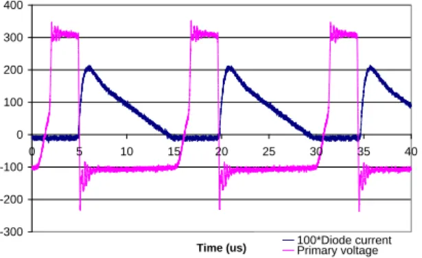
D Waveform analyzes
The last step consists in assessing the way to command the DC/DC conversion with a waveform analysis. We examine the diode current (x 100) and the primary voltage of the transformer, as shown in fig. 8.
-300 -200 -100 0 100 200 300 400 0 5 10 15 20 25 30 35 40
Time (us) 100*Diode currentPrimary voltage Figure 8 : Analyzing the command.
The switch begins to conduct when the current passing through the diode reaches zero. These waveforms are a feature of self-oscillating mode.
4. Modelling power supply devices With these specifications, we are able to create a model of losses for the typical power supply. Investigating DC local distribution network means to model only DC/DC converters, therefore we present model of losses inside a flyback SMPS, as shown in fig. 9, controlled by self oscillating mode. This model takes the switch losses (conduction and commutation), the losses of the passive elements, and the magnetic losses into account.
Figure 9 : Electrical scheme considered for modelling.
A Equations of flyback SMPS
The self oscillating mode induces a power control by the switching frequency. Moreover, the power demands of the load is an input for our model, thus we could easily calculate this frequency: 2 2
)
*
1
(
*
*
²
*
2
1
DC s s sV
m
V
P
L
m
V
T
f
All the losses inside DC/DC converters depend on current passing through the primary and secondary of the transformer (i1, i2). In all
electronic appliances, the voltage output of power supply (VS) should be considered as
constant, therefore the duty cycle is constant too. Consequently we could simply express these currents:
L
T
V
I
DC*
2
*
²
*
1
3 * * 3 1
L T V I DC RMS s sV
P
I
2
3 1 * * * * 2
L m T V I DC RMSWith these equations, we could also establish losses inside the different components of flyback SMPS.
B Losses of the switch
Currently, the switches use in such ranges of frequency and voltage could be MOSFETs or IGBTs. As our future study tends to reduce input voltage of power supply devices, we keep up only MOSFET switch for our model. Losses inside MOSFET could be summed up by two terms: conduction losses and switching losses. Conduction losses could be easily determined by neglecting the forward voltage, through the following equation where Rton is the static
drain-source on resistance.
²
P
MOSconduction
R
ton
I
1RMSFor switching losses, we suppose that this loss is due to capacitance between the gate and the drain of the switch. This capacitance is charged and discharged from 0 to VDC with the average
primary current through the resistance of the gate Rg. [9] express this loss by:
gs com gd g DC
V
V
Q
R
V
I
T
1 switching MOS1
P
ΔQgd is the charge contains in the intrinsic
capacitance Cgd and Vcom is the output voltage of
the switch driver.
C Losses of the diode
Like the switch, losses inside a diode could be divided in two parts. With piece-wise linear model, conduction losses depend on forward
resistance and forward voltage drop (Rd_f, Vd_f)
through the formula:
²
P
diode conduction
V
don
I
2
R
don
I
2RMS Switching losses depends on fluctuation of current. The self oscillating mode induced negligible switching losses.D Losses of the magnetic component
These losses can be separated in two terms: conduction losses and magnetic losses. Conduction losses can be expressed by:
²
²
P
magneticconduction
R
1
I
1eff
R
2
I
2effR1 and R2 are respectively primary and
secondary resistances. Magnetic losses are a combination of eddy current losses and hysteresis losses. We neglected skin and proximity effect losses. Each loss depends on the frequency f and the excursion of magnetic field ΔB and they are expressed by:
2
)
( B
f
P
ec
P
h
(
f
B
)
2In first time, we neglect variation of magnetic losses, in relation with power demands, and we consider it equal to a constant.
E. Others losses
We should also consider losses inside filtering element and command. Inside power supply devices that we have studied, filtering devices were a first order filter composed of a resistance and a capacitance. With the different currents passing trough filtering resistance and capacitance (IR, IC), we calculate losses with the
expression: 2 R f R
R
I
P
P
C
ESR
I
C2 The consumption of power supply devices without any load is considered as the power requirement of command system (control circuits and MOS gate driver consumption).F. Model reliability
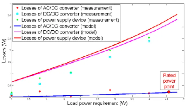
Before generalizing this model to other electronic devices, we compare our model with experimental measurement, as shown in fig. 10.
Figure 10 : Model vs measurements, comparison of losses for a mobile phone charger.
The differences between model and measurements for DC/DC converter can be explained by our hypothesis which considered magnetic losses as a constant. Its influence is predominant for small power demands. This approximation will be corrected before future simulation on voltage level. This model brings the distribution of losses inside power supply devices too, as shown in fig. 11.
Losses of filtering after AC/DC stage
5% Losses of diode bridge rectifier 1% Losses of filtering after DC/DC stage 24% Losses of DC magnetic componant 27% Losses of DC switch 16% Losses of command system 1% Losses of DC diode 26%
Figure 11 : Distribution of losses in a mobile phone charger at rated operating point.
Currently, the main losses are at the DC/DC stage due to the important difference between entrance and output voltage (from 325V to 5 V for a mobile phone charger). By using DC local network, we could reduce input voltage and thus constraints on semiconductor and magnetic components.
5. A first DC network simulation After the validation of our model, we extend it to other electronic appliances. We want to make a first simulation of a multimedia workstation composed of a laptop, a printer, a scanner, a phone, a mobile phone, an internet terminal. Firstly, we don’t want to change the components chosen by the manufacturer. Therefore we compare a current distribution network with a 320V DC one (voltage presents after the rectifier in power supply devices of electronic apppliances). In addition to power profile, which is measured during characterization process, we
need statistics about classical use of these devices. Paper [10] proposes a precise study about multimedia loads including power profile, use duration, consumption of sleeplessness. With this data we are able to design typical power profile for each load for one day, as shown in fig. 12.
Figure 12 : Typical power profile for a multimedia workstation at home.
These profiles are shown with normalized power (to rated power of each power supply). Almost all electronic devices are simultaneously switched on and forget to totally switch off (inducing consumption of sleeplessness) when we stop to use. With this data we are able to calculate energy consumption of our multimedia workstation for one day, as shown in fig. 13.
Figure 13 : Daily losses of a multimedia workstation.
It’s important to notice that our assumption about the constancy of magnetic losses generate overestimated energy losses. However the difference between the today distribution and the 320V DC one remain minimal (20 W.h). Moreover, only losses of converters are taken into account. Inside a building, we should add losses inside a general inverter placed upstream from the local distribution network if the loads are supplying by the grid, but so losses of a MPPT DC/DC converter of the photovoltaic installation. In each case, conduction losses inside wiring should be added too. According to efficiency of converters, the 320VDC distribution
network is not interesting because the gap between network voltage and end-user voltage is too high and realized by DC/DC converter
again. Nevertheless we can’t exclude it before an assessment of its Global Energy Requirement like we will present further. Whereas the grid voltage is fixed by standards, the output voltage of photovoltaic systems can be chosen. Moreover, input voltage of rectifier could be easily modified by using a transformer which presents an efficiency close to 100% (if current passed through it is sinusoidal). According to these observations, it seems to be interesting to study other voltage levels.
6. Future study of DC voltage level
A Global aim of the study
As we present in first part, DC distribution scheme seems to be obvious but this pertinence should be checked. Before comparing the DC distribution scheme with the classical one, we need to find the optimal DC voltage level(s). But is there an optimum value? Classical studies achieved optimization according to electrical losses for wires or efficiency at rated operating point for converters, but think different. If we realized a new distribution scheme which saves electric energy, and so primary energy, during its use, we don’t want that its fabrication induce bigger energy consumption than the classical scheme. Therefore, we will use a Life Cycle Assessment (LCA) to quantify environmental impact of DC distribution network. Rather than analysing all criteria included in LCA, we will focus on Global Energy Requirement (GER) which takes primary energy consumption during all the cycle life into account. This study could be divided into three steps. Firstly, we will find a model for the variation of losses in relation to voltage levels. Secondly, we will determine the GER of the different component in comparison with voltages levels. And finally, we could optimize a DC distribution network and compare with the actual one.
B Variation of losses in relation with voltage levels
As we presented it in part 4, losses are related to characteristic parameters such as resistance, forward voltage etc; the optimization of voltage levels involve doing new dimensioning process at each voltage and thus change components. Actual electronic components are designed for voltage levels which are fixed by classical appliances forming a non continuous range. In order to compare a classical voltage with a custom-made voltage on the same frame of
reference, we need to find a model for the variation of characteristic parameters with constraints of the components (voltage, current, frequency…). Our reasoning will be to study actual component in all their range to deduce our models in order to apply them in our optimization process.
C Global Energy Requirement of electronic components
Characteristic parameters are related to the size of active material inside the components. Its dimension gives us information on the quantity of active material. We will base our analysis of GER on the energy cost of active materials and energy consumption during its use. Like for the variation of losses in relation with voltage levels, we study actual components in order to model the quantity of active materials in relation with voltage levels. In addition to this quantity, LCA databases allow finding the energy impact of materials.
D Optimization and comparison of local distribution network
As we proposed sooner, the cost function for the optimization process will be based on GER. Moreover, we will choose two case-studies: a household and an office. Before, we need to develop models for other types of load, choose a topology for a global AC/DC converter placed between grid and DC distribution network and finally create a model for to photovoltaic converter. The aim is to conclude about DC distribution network and its performance functions in the sizing of PV installations.
7. Conclusion
DC local distribution network appears obvious given the needs of actual loads and the influence on grid of new components such as renewable energies and electric vehicles. We propose to begin by proving this supposition on electronic devices, and present a characterization process which allows creating a model of losses for converters. Findings of these characterizations induced a focus on flyback switch-mode power supply using self oscillating modes and pointed up the poor efficiency of actual DC/DC converters. After we checked the reliability of the model, we extended it to several electronic devices to conclude that the removal of the AC/DC stage in actual power supply devices doesn’t allow an important energy saving. Our first results induce us to explore other voltage
levels. Therefore, we have exposed our future study on voltage levels. We propose to find an optimal voltage level by design optimizations of the power supplies in relation with the global energy requirement. This approach will be extended to other converters and simulation of two different case-studies will be achieved to conclude about the feasibility of DC local distribution network.
References
[1] Agence Locale de l’Energie de l’agglomération lyonnaise, “L’ancien c’est l’avenir ? Ou comment rendre économe en énergie un logement existant”, in ALE infos, Vol 23, 2008.
[2] D. Crudele et al, “Commercial and industrial applications getting ready for direct current power distribution,” in IEEE Power Systems
Conference and Exposition PSCE'04, New
York: 2004.
[3] H. Nasution and M. Nawi Wan Hassan, “Potential electricity savings by variable speed control of compressor for air conditioning systems,” in HNICEM,
Manilia, Spain, 2005.
[4] A. Sannino, et al, “Feasability of a DC network for commercial facilities,” in IEEE
Transactions on Industry applications, vol.
39, Oct. 2003.
[5] M. Starke et al, “AC vs. DC Distribution A loss comparison,” in IEEE PES T&D, Chicago, USA, 2008.
[6] K Engelen, et al, “The Feasibility of Small-Scale Residential DC Distribution Systems,” in IEEE Industrial Electronics Society, CNAM Paris, France 2006.
[7] P-W Lee et al, “Power distribution system for future home,” in IEEE International
conference on power electronics and drive systems, Hong-Kong, China, 1999
[8] M. Sechilariu, “Production décentralisée d'énergie électrique d'origine renouvelable et éclairage basse consommation,” in IBPSA, INSA Lyon, France, nov. 2008
[9] P. Leturcq, “Semi-conducteurs de puissance unipolaires et mixtes (partie 2)”, in TI
D3109, 2002
[10] Enertech, “Mesure de la consommation des usages domestiques de l’audiovisuel et de l’informatique”, in Rapport final projet
![Figure 1 : Energy consumption distribution inside buildings according to buildings standards or eco-labels [1]](https://thumb-eu.123doks.com/thumbv2/123doknet/12880626.369999/2.892.473.787.886.1025/figure-energy-consumption-distribution-buildings-according-buildings-standards.webp)