HAL Id: cea-01974229
https://hal-cea.archives-ouvertes.fr/cea-01974229
Submitted on 8 Jan 2019
HAL is a multi-disciplinary open access
archive for the deposit and dissemination of
sci-entific research documents, whether they are
pub-lished or not. The documents may come from
teaching and research institutions in France or
abroad, or from public or private research centers.
L’archive ouverte pluridisciplinaire HAL, est
destinée au dépôt et à la diffusion de documents
scientifiques de niveau recherche, publiés ou non,
émanant des établissements d’enseignement et de
recherche français ou étrangers, des laboratoires
publics ou privés.
Methodology to Separate Channel Conductions of Two
Level Vertically Stacked SOI Nanowire MOSFETs
Bruna Cardoso Paz, Mikael Casse, Sylvain Barraud, Gilles Reimbold, Maud
Vinet, Olivier Faynot, Marcelo Pavanello
To cite this version:
Bruna Cardoso Paz, Mikael Casse, Sylvain Barraud, Gilles Reimbold, Maud Vinet, et al.. Methodology
to Separate Channel Conductions of Two Level Vertically Stacked SOI Nanowire MOSFETs.
Solid-State Electronics, Elsevier, 2018, 149, pp.62-70. �10.1016/j.sse.2018.08.012�. �cea-01974229�
Methodology to Separate Channel Conductions of Two Level Vertically Stacked SOI
Nanowire MOSFETs
Bruna Cardoso Paz1, Mikaël Cassé2, Sylvain Barraud2, Gilles Reimbold2, Maud Vinet2, Olivier Faynot2
and Marcelo Antonio Pavanello1
1Department of Electrical Engineering, Centro Universitário FEI, São Bernardo do Campo, Brazil 2Département des Composants Silicium – SCME/LCTE, CEA-LETI Minatec, Grenoble, France
bcpaz@fei.edu.br
Abstract—This work proposes a new method for dissociating both channel conductions of two levels vertically stacked inversion mode nanowires (NWs) composed by a Gate-All-Around (GAA) level on top of an Ω-gate level. The proposed methodology is based on experimental measurements of the total drain current (IDS) varying the back gate bias (VB), aiming the extraction of carriers’ mobility of each level
separately. The methodology consists of three main steps and accounts for VB influence on mobility. The
behavior of non-stacked Ω-gate NWs are also discussed varying VB through experimental measurements
and tridimensional numerical simulations in order to sustain proposed expressions of mobility dependence on VB for the bottom level of the stacked structure. Lower mobility was obtained for GAA in
comparison to Ω-gate. The procedure was validated for a wide range of VB and up to 150°C. Similar
temperature dependence of mobility was observed for both Ω-gate and GAA levels.
Keywords—vertically stacked nanowires; SOI; mobility; back gate bias; tridimensional numerical simulations; temperature
I. INTRODUCTION
Multiple gate MOSFETs have attracted the interest of semiconductor industry due to strong immunity against short channel effects and great scalability because of improved electrostatic coupling [1]–[3]. Ω-gate and GAA MOSFETs with nanoscale cross-section, also denominated as nanowires, turned into candidates for future technological nodes due to their performance [2], [4]. Such devices are fabricated with close dimensions for both silicon thickness (HFIN) and fin width (WFIN), around 10nm. In order to
fulfill higher drive current requests and increase the on-state current by footprint (ION/WFIN), nanowires
have been recently vertically stacked thanks to advances on tridimensional integration process [5]–[7]. Once vertically stacked NWs present overall channel width (Weff) proportional to the number of stacked
levels (or beams), these devices have higher aspect ratio, which is necessary for NWs to reach industrial targets for saturation current [8].
The implementation of vertically stacked NWs brings technological challenges such as the reduction of intrinsic parasitic capacitance and integration of carriers’ mobility boosters. These problems have been recently addressed by the innovative structure fabricated at CEA-LETI, combining inner spacers and SiGe source/drain in vertically stacked p-type NW MOSFETs [7]. The overall effective mobility of these stacked NWs was investigated in [9], while [10] presented a methodology to perform individual electrical characterization of each NW level including explicit expressions for the low field mobility (µ0) and
the channel conductions of staked multiple gate devices using VB [11] does not take into account transport
parameters dependence on the back bias, the methodology proposed in [10] improves [11]. In this work, we extend [10] by including experimental measurements and tridimensional numerical simulations of non-stacked Ω-gate NWs varying VB in order to explain physical effects in the potential, electric field and
holes mobility under different back bias conditions. Such explanations are important to understand the vertically stacked NWs behavior and, therefore, sustain the expressions used for mobility dependence on VB in the proposed methodology for individual electrical characterization, once the bottom level of the
stacked structure is Ω-shaped. Moreover, this work brings deeper details of the proposed methodology step by step, so it can be easily reproduced. Discussions concerning temperature influence on VB
dependence are also presented in this work.
The paper is organized as follows: Section II details the devices characteristics for both stacked (Section II-A) and non-stacked NWs (Section II-B). Section III presents the main physical effects of applying VB
on mobility of non-stacked Ω-gate NWs (Section III-A), the proposed methodology to dissociate channel conductions of two levels vertically stacked NWs (Section III-B) and temperature influence on VB
dependence (section III-C). Finally, Section IV points out the main conclusions of this work.
II. DEVICES CHARACTERISTICS
A. Vertically stacked NWs
Transistors are [110]-oriented vertically stacked p-type inversion mode nanowires MOSFETs with two levels, being the bottom level Ω-gated and the top level GAA. Figure 1 shows Transmission Electron Microscopy (TEM) images of the studied stacked NWs cross section (a) and the longitudinal section (b). Usually the vertically stacked NWs have an Ω-gated bottom level while the upper levels are GAA because the fabrication process starts from Fully Depleted (FD) SOI wafers. The first Si channel lies on top of the buried oxide and the upper channels are fabricated on top of SiGe layers, which are replaced after selective etching, giving place to the surrounded gate stack of GAA NWs. From Figure 1.a, it is possible to note that the front gate of the bottom NW is electrostatically coupled with the back gate. Although narrow triple gate MOSFETs present lower back gate bias (VB) influence in comparison to
planar MOSFETs [12], the potential lines coming from the back gate manage to reach the Si channel through the interface between Si and buried oxide. On the other hand, the top NW is independent of VB
because it is surrounded by the gate stack. Despite the lower impact of VB over the electrical parameters
of narrow Ω-NWs, since the bottom NW is VB dependent while the top one is VB independent, back
biasing can be used as a tool to separate the channels conduction. The interest of using back bias in this work is attached to the methodology proposed in Section III to perform individual electrical characterization for future technology optimization.
Devices have been fabricated at CEA-LETI, starting from Silicon-On-Insulator (SOI) wafers with 145nm buried oxide thickness (tBOX) and using a replacement metal gate (RMG) process to obtain a gate stack
composed by HfO2/TiN/W, resulting in effective oxide thickness (EOT) of 1.15nm. Each level has a
10nm thick undoped Si channel and both levels are attached by common metal gate and Si0.7Ge0.3:B
fabricated in multi finger structures with 50 fins in parallel and channel length (L) of 100nm. Further fabrication details of the stacked-NWs studied in this work can be found in [7].
(a) (b)
Figure 1. Vertically stacked SOI nanowire cross section (a) and longitudinal section (b) TEM images.
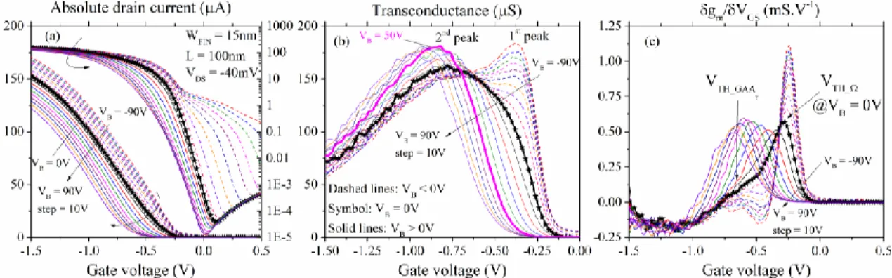
Figure 2 presents drain current, IDS (a), transconductance, gm (b), and its derivative, δgm/δVGS (c), as a
function of the front gate voltage (VGS) for stacked NW with WFIN = 15nm and L = 100nm, at low drain
voltage (VDS = -40mV), varying VB from -90V to 90V. In these figures the curves with symbols refer to
VB = 0V. During the measurements, VB was applied at the substrate of the whole wafer, which is isolated
from the active channels by the thick buried oxide. Although ±90V may seem like extremely high bias condition, it is important to remember that tBOX = 145nm. For simplicity, considering the same linear
potential drop across the front and back interface, 90V applied at 145nm-thick oxide would correspond to ~0.7V applied at the same oxide with thickness of 1.15nm. The applied back bias values must be adjusted according to the technology of the studied SOI MOSFET to avoid reliability and degradation issues due to high vertical electric field.
Figure 2.a shows expected shift of curves to the left as VB increases due to threshold voltage (VTH)
variation. Moreover, small back conduction is noted in the subthreshold region of logarithmic curves for negative back gate values.
Figure 2.b shows two distinguished peaks for gm depending on VB. Results suggests some VTH mismatch
between bottom and top levels once the two peaks are still slightly perceived at VB = 0V, the first for VGS
-0.4V and the second for VGS -0.75V. Two effects are observed and overlapped. First, the gm peak
decreases with VB increase for negative values (dashed lines) and for high positive VB (higher than 50V).
Second, for sufficiently low VB a second gm peak appears at higher VGS voltages. This second gm peak
presents the opposite behavior from 0V < VB < 50V. The effect that explains the first behavior is related
to the effective mobility changing with VB, which will be detailed in Section III-A. The second effect
happens due to VTH mismatch, the closer both threshold voltages get, the higher the transconductance,
once both conductions are overlapped from their starting point, where no strong mobility degradation is observed yet due to surface roughness.
Figure 2.c confirms the existence of VTH mismatch between top and bottom levels at VB = 0V. The
constant peak in Figure 2.c is insensitive to VB and related to the threshold voltage of the top NW
(VTH_GAA), while the other one is sensitive to VB and corresponds to the threshold voltage of the bottom
Ω-NW (VTH_ΩG). No peak is observed due to back conduction because of its small contribution, as
Ti
Step 4-5.
Release of Si wires and
RMG module (HfO2/TiN/W)
Ti Si Hf Ti W
(b)
(a)
Omega-Shaped Gate bottom wire to maintain a good electrostatic integrityindicated in Figure 2.a and expected in narrow Ω-NWs. VTH mismatches could be related to charge traps
in the GAA-NW, which presents much lower VTH and is more susceptible to defects after RMG process
fabrication in comparison to the bottom level.
Figure 2. |IDS| (a), gm (b) and |δgm/δVGS| (c) as a function of VGS for stacked NW with WFIN = 15nm, L =
100nm, VDS = -40mV and VB from -90 to 90V.
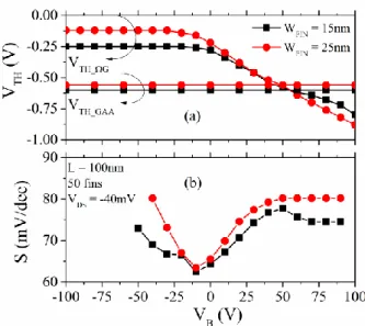
Figure 3 shows threshold voltage, VTH (a), and subthreshold slope, S (b), as a function of VB for stacked
NWs with WFIN = 15 and 25nm and L = 100nm, at VDS = -40mV. The threshold voltage has been
extracted by the double derivative method. The subthreshold slope has been extracted from ∂VGS/∂(logIDS) curves, considering an average around the minimum value to account for ~1-2 decades of
IDS. Figure 3.a presents VTH for both bottom (VTH_ΩG) and top (VTH_GAA) NWs extracted from ∂gm/∂VGS
peaks in Figure 2.c. Threshold voltage mismatches between bottom and top NWs are found to be 0.32 and 0.34V for WFIN = 15 and 25nm, respectively, at VB = 0V. It is observed that VTH_ΩG exhibits a plateau for
VB < -10V because the back interface of the bottom NW operates in inversion, which degrades the overall
subthreshold slope. For VB > -10V, the bottom NW enters in full depletion and VTH_ΩG decreases linearly
with VB increase, while VTH_GAA remains constant once the top NW is VB independent. Due to thin silicon
layer, the bottom NW never reaches accumulation [14]. At VB = 50V, VTH_ΩG = VTH_GAA. The NW level
with lower |VTH| conducts at lower |VGS| and, therefore, dominates the subthreshold slope behavior of the
overall structure. The IDS of the NW level with higher |VTH| is orders of magnitude lower comparing to the
other NW level, at a given VGS in the subthreshold regime, so its subthreshold characteristic is hidden in
the I-V curve of the overall structure. For VB > 50V, |VTH_ΩG| > |VTH_GAA|, thus the subthreshold
characteristics observed in IDS are determined by the GAA-NW. This explanation is consistent with
Figure 3. VTH and S as a function of VB for stacked NWs with WFIN = 15 and 25nm, L = 100nm and VDS
= -40mV.
B. Non-stacked Ω-NWs
Once the overall behavior of the stacked structure varying VB is determined by the bottom level,
non-stacked Ω-NWs will be also studied in order to better understand the non-stacked NWs behavior with VB.
Transistors are silicon [110]-oriented Ω-NWs SOI MOSFETs in multi finger structures with 10 fins in parallel, HFIN = 11nm, L = 100nm, tBOX = 145nm and gate stack composed by HfSiON/TiN (EOT =
1.4nm). Figure 4 shows TEM image (a) and schematic (b) of the devices fabricated at CEA–Leti [15], [16].
(a) (b) Figure 4. Non-stacked SOI NW cross section TEM image (a) and schematic (b).
Figure 5 presents IDS (a) and gm (b) as a function of VGS for non-stacked NW with WFIN = 15nm and L =
100nm, at VDS = -40mV, varying VB from -80V to 80V. Although Figure 5.a shows the same behavior for
IDS with VB as in Figure 2.a, a single gm peak is observed in Figure 5.b, once the non-stacked transistor is
a single level NW. As VB increases, the maximum gm decreases in a practically constant rate, suggesting
stronger mobility degradation effect as VB gets higher. Such behavior is coherent with results in Figure
2.b for negative back bias. The physical effects resulted from VB influence will be discussed in details in
Figure 5. |IDS| (a) and gm (b) as a function of VGS for non-stacked NW with WFIN = 15nm, L = 100nm, VDS
= -40mV and VB from -80 to 80V.
III. RESULTS AND DISCUSSION
A. Back bias dependence for non-stacked Ω-NWs
Tridimensional numerical simulations were performed in Sentaurus Device Simulator, from Synopsys [17]. Same dimensions and materials as in fabricated Ω-NWs were used to build the simulated structures in Sentaurus Process [18], as shown in Figure 6. Transport parameters of Inversion and Accumulation
Layer Mobility Model were calibrated according to measured I-V curves in Figure 5. Fixed charges of
6×1012cm-2 were placed at the silicon/buried oxide interface to adjust the threshold voltage of the back
interface. Moreover, simulations account for the following physical effects: mobility degradation due to vertical and lateral electric fields, Shockley-Read-Hall effect and Auger recombination, bandgap narrowing dependence on temperature and doping, Fermi statistics and density gradient quantization.
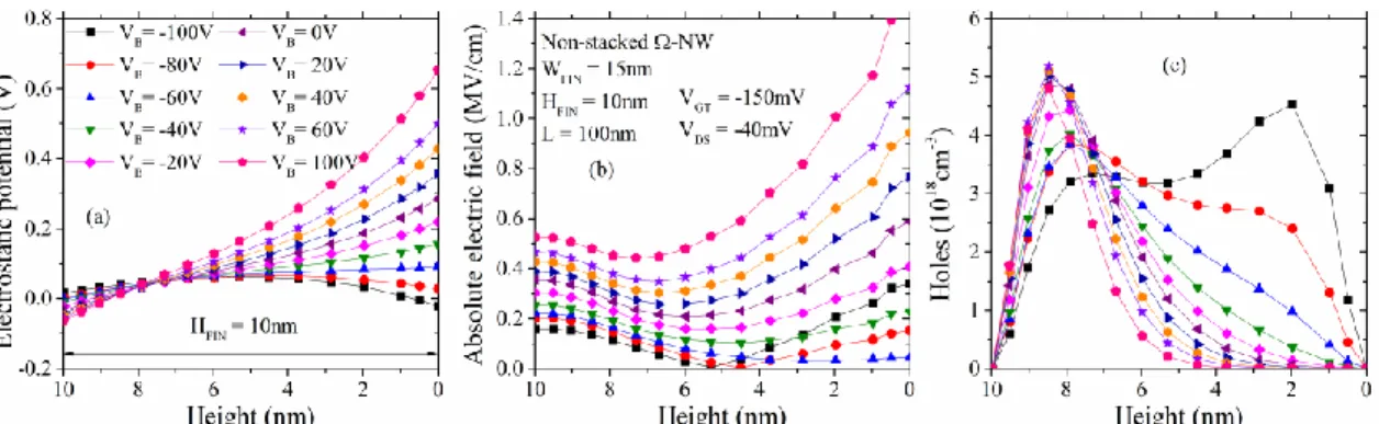
Figure 6. Ω-gate nanowire TCAD structure originated from Sentaurus Process and used for tridimensional numerical simulation. Longitudinal section (a), perspective (b) and cross section (c).
Figure 7 presents simulated results extracted along the vertical cut of non-stacked NW cross-section for the electrostatic potential (a), electric field (b) and holes concentration (c) at gate voltage overdrive (VGT
= VGS − VTH) of -150mV, VDS = -40mV and VB ranging from -100V to 100V. Height = 0nm indicates
silicon/buried oxide interface and Height = 10nm indicates silicon/front oxide interface. Figure 7.a shows inversion at the front gate for all VB values and back inversion for VB = -80V and -100V, where the back
bias is negative enough to induce back conduction. The inflection point that separates inversion from depletion appears around 7.5nm far from the silicon/buried oxide interface indicating that inversion layer occurs up to 2.5nm far from the front interface. These effects are clearer in Figure 7.c, where the front and back conductions are observed by the peaks of holes concentration, around 2nm close to the front interface for VB from 100V to -60V and then a second peak appearing close to the back interface for VB =
-80V and -100V. Figure 7.a also shows the electrostatic potential decrease with VB increase at the front
interface and opposite behavior at the back interface. Potential changing is reflected in the holes concentration in Figure 7.c, where the peak at the front interface increases with VB increase at the front
interface and opposite behavior is verified at the back interface.
Figure 7.b shows the electric field increase with VB increase, which leads to stronger mobility degradation
[1]. Moreover, it is observed in Figure 7.c that the conduction peak moves into the center of the silicon layer with VB reduction. The center of the transistor should present higher effective mobility due to
smaller electric field (see Figure 7.b) and lower surface roughness scattering in the case of fabricated devices. Indeed, as discussed in [19], the inversion charge distribution in the channel is modulated by VB.
Therefore, after the analysis of Figure 7, it is possible to state that the effective mobility is expected to reduce with VB increase because of holes concentration increase and its position change along the NW
channel.
Figure 7. Simulated results for the electrostatic potential (a), electric field (b) and holes concentration (c) as a funtion of fin height for non-stacked NW with WFIN = 15nm, HFIN = 10nm, L = 100nm, VDS =
-40mV, VGT = -150mV and VB from -100 to 100V.
Figure 8 shows holes mobility along the vertical cut of non-stacked NW cross-section at VGT = -150mV,
VDS = -40mV and VB varying from -100V to 100V. Holes mobility follows the inverse of the electric field
behavior, increasing with VB decrease and being higher in the center of the silicon layer. In practice,
comparing to mobility closer to the front oxide interface, mobility in the center and closer to the buried oxide of fabricated devices must be even higher than those in simulations, because of smaller defects and better interface quality at the second interface [20], which are not considered in these simulations.
Besides, it is observed that holes mobility closer to the buried oxide decreases with VB decrease for VB =
-80V and -100V, which happens because of holes concentration increase in this region, where some back conduction starts to appear, as verified in Figure 7.c.
Figure 8. Simulated results for holes mobility as a funtion of fin height for non-stacked NW with WFIN =
15nm, HFIN = 10nm, L = 100nm, VDS = -40mV, VGT = -150mV and VB from -100 to 100V.
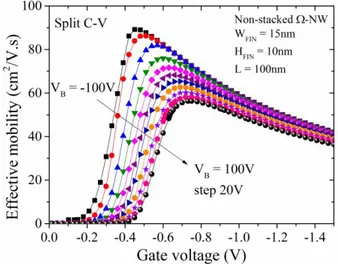
Figure 9 shows µeff as a function of VGS for simulated non-stacked NW varying VB from -100V to 100V.
Results were calculated by split C-V technique [21]. As expected from gm results in Figure 5 and
explained by results in Figure 7, the effective mobility shows significant degradation with VB increase (up
to 37% considering maximum mobility variation from VB = -100V to 100V). Curves shift to the right
indicate VTH decrease with VB increase, where ∆VTH/∆VB has been extracted around -1.1mV/V from I-V
simulations. Similar result has been obtained from measurements in Figure 5, where ∆VTH/∆VB =
-1.0mV/V. Figure 9 also shows that µeff differences among curves with different VB reduces with VGS
increase, indicating that first order mobility degradation coefficient (θ1) increases with VB reduction. This
assumption is confirmed in Section III-B after complete extraction of mobility parameters through the proposed methodology.
Figure 9. Simulated results for µeff extracted by split C-V method as a funtion of VGS for non-stacked NW
with WFIN = 15nm, HFIN = 10nm, L = 100nm, VB from -100 to 100V.
Symbols in Figure 10 show extracted µ0 as a function of VB for simulated and measured non-stacked
NWs. Dashed lines indicate linear fitting of data points. For simulations, results were obtained by taking the maximum µeff from Figure 9, calculated from split C-V method. For measurements, as devices present
small capacitance level, split C-V could not be applied and results were obtained through Y-function method [22], where the low field mobility represents µeff at VGT = 0V. Once Y-function method do not
predict Coulomb scattering mobility degradation [23], Y-function µ0 results are expected to be slightly
higher than those extracted by split C-V. Independent on the methodology, both simulations and measurements can be represented by linear expressions with acceptable errors (smaller than 5% and 8% for simulations and measurements, respectively). Moreover, similar µ0 dependence on VB is observed for
both simulations (slope = -0.17cm2/V2.s) and measurements (slope = -0.21cm2/V2.s), as expected after I-V
calibration. Higher slope obtained for measurements could be related to the better interface quality at the second interface in comparison to the first interface, which increases even more the effective mobility when the inversion channel shifts to the center of Si layer.
Figure 10. µ0 as a funtion of VB for simulated and measured non-stacked NWs with WFIN = 15nm, HFIN =
10nm, L = 100nm and VDS = -40mV. Dashed lines indicate linear regression of data points, where errors
obtained are smaller than 5% and 8% for simulations and measurements, respectively.
B. Methodology for mobility dissosiation in stacked NWs
Once measured IDS – VGS curves varying VB are obtained for stacked NWs, it is possible to dissociate the
bottom and top levels mobility contribution in 3 steps, by using the following proposed methodology. In order to show the extended validity of the proposed methodology, a wide range and large number of VB
values were taken into account. Since linear equations are used to express mobility dependence on VB, the
technique can also be successfully employed with much fewer IDS – VGS curves and lower VB values.
Concerning the range of geometrical parameters for the application of the proposed methodology, WFIN
and HFIN must be equal or larger than 10nm, so quantum effects can be considered negligible. Moreover,
Step 1.
In order to obtain the overall parameters related to the sum of contributions of Ω- and GAA-NWs, Y-function method is applied to the measured IDS. At this step, VGS range where Y-function is applied must
be chosen to capture the back bias influence on low field mobility of the Ω-NW. From the dashed lines in Figure 2.b, where VB < 0V, it is observed that gm peak significantly decreases with VB increase on the
same way as observed in Figure 5.b for non-stacked NW. Moreover, Figure 3 shows that negative values of VB lead to constant VTH_Ω and VTH_GAA. When both top and bottom levels present constant threshold
voltage with VB variation, IDS_ΩG and IDS_GAA do not shift along VGS. In this case, the overlap between the
two currents must not influence the extraction of VB dependence. Therefore, gm variation at negative VB
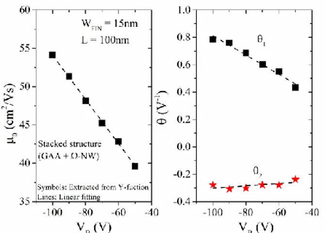
should be only linked to µeff effect. Figure 11 shows µ0 and first and second order mobility degradation
coefficients (θ1 and θ2) extracted from Y-function, varying VB. The gate capacitance per unit of area
(COX) and the effective channel width (Weff) used in Y-function methodology are 2.7×10⁻⁶F/cm2 and
8.5×10⁻⁶cm, respectively. Symbols represent the extracted results and lines indicate linear regression of
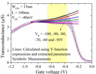
data points. Figure 12 shows gm as a function of VGS for the stacked NW, where symbols indicate the
measurements and the lines were obtained from Y-function expressions, using the extracted parameters shown in Figure 11. The agreement among lines and symbols in Figure 12 indicates that VGS range
chosen for the application of the Y-function methodology (highlighted in yellow) clearly captures gm
variation with VB.
Figure 11. Step 1. Overall low field mobility (a) and mobility degradation coefficients (b) as a function of VB for vertically stacked NWs with WFIN = 15nm and L = 100nm. Results were extracted from the total
IDS, which corresponds to the characteristics of the whole stacked structure, i.e. sum of GAA and Ω-NW
Figure 12. Step 1. Measurements and Y-function model results of gm as a function of VGS for stacked NW
with WFIN = 15nm, L = 100nm and VDS = -40mV. The area painted in yellow indicates the VGS range
chosen to apply the Y-function methodology.
As previously discussed in Section III-A, a linear dependence between mobility parameters and VB is
expected for Ω-NWs. Moreover, linear expressions can be considered with small errors for a wide VB
range. Therefore, the bottom level first and second order mobility degradation coefficients and low field mobility can be written as θ1,ΩG = Aθ1 + aθ1×VB; θ2,ΩG = Bθ2 + bθ2×VB and µ0,ΩG = Cµ0 + cµ0×VB. On the
other hand, the GAA level mobility parameters are constants and given by θ1,GAA, θ2,GAA and µ0,GAA.
From Figure 11, the linear fittings of data points lead to the extraction of slope and intercept, where the slopes indicate the VB dependence of the parameters. As the GAA-NW contribution does not change with
VB, slopes extracted from Figure 11 can be exclusively attributed to the bottom Ω-NW and correspond to
aθ1, bθ2 andcµ0.
Step 2.
For VB ≥ 0, as there is no back conduction, the stacked NW drain current can be written as
IDS(VB ≥ 0) = IDS,ΩG(VB) + IDS,GAA (1)
where the drain currents of Ω- and GAA-NWs, at low VDS, are given by
IDS,ΩG(VB)= Weff,ΩG×COX L μ0,ΩG(VB)×VGT,ΩG(VB)×VDS 1+θ1,ΩG(VB)×VGT,ΩG(VB)+θ2,ΩG(VB)×VGT,ΩG2(VB) (2) IDS,GAA= Weff,GAA×COX L μ0,GAA×VGT,GAA×VDS
1+θ1,GAA×VGT,GAA+θ2,GAA×VGT,GAA2
(3)
Considering that mismatches of WFIN and HFIN between bottom and top levels are negligible, as suggested
by TEM images (Figure 1), the effective channel widths are Weff,ΩG = (2HFIN + WFIN) and Weff,GAA =
(2HFIN + 2WFIN). For the sake of simplicity, we approximate the Weff expression of the Ω-NW to the one
WFIN, which decreases Weff in few nanometers. Opposite effect is observed for the bottom surface, which
is partially surrounded by the gate. Since the opposite characteristics may compensate each other, the calculated Weff should not present strong deviation in comparison to the real dimension. Good accuracy is
desired when calculating Weff, because an error of +X% in Weff results in an error of –X% in µ0/(1 +
θ1VGT + θ2VGT2). This error of –X% should be distributed among the three parameters. For the studied
stacked NW with WFIN = 1.5×10⁻⁶cm and HFIN = 1.0×10⁻⁶cm, Weff,ΩG = 3.5×10⁻⁶cm and Weff,GAA = 5.0×10 -6cm.
Subtracting (1) at a given VB1 ≥ 0 from (1) at VB2 > VB1, the resulting current will only depend on IDS,ΩG,
once IDS,GAA is constant with VB and annulated by the subtraction. If the difference between the total
currents at two different VB values is called ∆IDS(VB), then
∆IDS(VB) = IDS(VB1≥0) – IDS(VB2>VB1) = IDS,ΩG(VB1) – IDS,ΩG(VB2) (4)
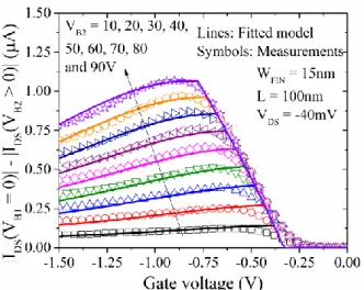
Fitting (4) to experimental measurements allow determining the remaining mobility parameters for the bottom Ω-NW, which are the intercepts Aθ1, Bθ2 and Cµ0. Figure 13 shows ∆IDS as a function of VGS for
VB1 = 0V and several positive VB2 values, ranging from 10V to 90V. Good agreement is obtained
comparing measurements and fitted expression (4).
Figure 13. Step 2. Measurements and model results of ∆IDS as a function of VGS for stacked NW with
WFIN = 15nm, L = 100nm and VDS = -40mV.
Step 3.
After step 2, IDS,ΩG can be fully calculated, once all parameters for the bottom level are determined.
Fitting IDS measurements to (1), it is possible to extract the top level parameters θ1,GAA, θ2,GAA and µ0,GAA.
Figure 14 shows IDS measured curves and fitted expression (1) for positive VB ranging from 10V to 90V.
It is important to keep positive VB values at this step because there is no back conduction component
comprised in the total current. Good agreement is obtained for all VB values comparing measurements
Figure 14. Step 3. Measurements and model results of |IDS| as a function of VGS for stacked NW with WFIN
= 15nm, L = 100nm and VDS = -40mV.
Figure 15 presents the schematics of the entire procedure, highlighting all the extracted parameters and respective steps.
Figure 15. Schematic representation of the proposed method highlighting steps 1 to 3.
Figure 16 presents the obtained parameters for both Ω- and GAA-NWs of the stacked structure. Similar µ0,ΩG is found by comparing the stacked bottom level (79 – 0.26VB) to the non-stacked Ω-NW in Figure
10 (80 – 0.21VB), corroborating with the validity of the proposed method. Lower µ0 is obtained for
GAA-NW in comparison to bottom Ω-GAA-NW, which could be related to the defects that might have shifted its VTH
(Figure 3). Besides, lower mobility is expected for GAA in comparison to Ω-shaped structures due to detrimental stronger contribution of (100)/[110] surface for holes [24].
Figure 16. Parameters extracted through the proposed methodology for stacked NWs with WFIN = 15nm
and L = 100nm.
In case of many GAA stacked levels over one Ω-gate level, it would still be possible to apply the proposed methodology and extract the mobility parameters of the Ω-NW. If an approximation where all GAA-NWs present similar characteristics (dimensions, defects and mobility scattering) can be considered reliable for a given technology, the mobility parameters could be also extracted for the GAA levels. Since uniformity for GAA-NWs is hard to obtain during the fabrication process of several stacked levels, the technique applicability would depend on how interesting the extraction of average behaviors for the GAA-NWs would be.
C. Temperature dependence for stacked NWs
By applying the proposed methodology in stacked NWs under different temperature conditions, it is possible to study the temperature dependence on the back bias influence on mobility. Stacked NWs have been measured from 25°C up to 150°C and µ0 has been extracted for both bottom and top levels through
the proposed method. It is important to mention that nanowires present quantum confinement effects at cryogenic operation [25], so the methodology should be no longer valid at very low temperatures. Figure 17 shows results of the low field mobility as a function of VB at different T, for the bottom Ω-NW with
WFIN = 25nm, L = 100nm and VDS = -40mV. It is observed the expected mobility decrease with T
increase [26], reducing from 68cm2/V.s (at 25°C and V
B = 0V) to 52cm2/V.s (at 150°C and VB = 0V),
which represents 21% of degradation. Lower mobility obtained for WFIN = 25nm (68cm2/V.s at 25°C and
VB = 0V) in comparison to WFIN = 15nm (79cm2/V.s at 25°C and VB = 0V, in Figure 16) is due to higher
(100)/[110] surface contribution, as already discussed in [9], [24]. Moreover, Figure 17 shows that µ0
slopes significantly decrease with T increase, suggesting stronger back bias influence at lower T conditions.
Figure 17. Extracted µ0,ΩG as a function of VB for bottom Ω-NW of stacked transistor with WFIN = 25nm,
L = 100nm and VDS = -40mV. Temperature varies from 25°C to 150°C.
Figure 18 presents µ0 as a function of T for both top and bottom NWs, indicating clear temperature
influence on µ0 dependence on VB. At VB = 0V, both Ω- and GAA-NWs present similar µ0 slope with
temperature variation (Δµ0/ΔT), -0.12cm2/V.s.°C and -0.11cm2/V.s.°C, respectively. As VB decrease
pushes the inversion channel to the center of the silicon layer, as studied in Figure 7.c, reduced surface roughness contribution and higher phonon scattering contribution are expected. Unlike surface roughness scattering, phonon scattering is high T dependent, which leads to strong µ0 T-dependence with VB. For
positive VB, carriers are pushed against the interface and surface roughness limited contribution is
dominant. Since this mobility degradation mechanism is T independent, µ0 is almost constant varying T.
The same trend for Δµ0/ΔT with VB variation has been observed in non-stacked Ω-NWs MOSFETs, as
indicated in Table 1. Results of Δµ0/ΔT for the bottom level of stacked NW in Figure 18 and non-stacked
Ω-NW with WFIN = 20nm, L = 100nm have been summarized in Table 1 at VB = -30, 0 and 30V. Mobility
T-dependence has been evaluated considering measurements with T ranging from 25°C to 150°C.
Figure 18. Extracted µ0 as a function of T for both top GAA- and bottom Ω-NWs of stacked transistors
Table 1. Δµ0/ΔT for VB = -30, 0 and 30V for the bottom level of stacked NW and non-stacked Ω-NW
with similar dimensions.
Δµ0/ΔT (cm2/V.s.°C) Bottom level Ω-NW WFIN = 25nm, L = 100nm Non-stacked Ω-NW WFIN = 20nm, L = 100nm VB = -30V -0.15 -0.27 VB = 0V -0.12 -0.21 VB = 30V -0.09 -0.15 IV. CONCLUSIONS
This work detailed the effect of back bias in Ω-gated NWs through experimental measurements and tridimensional numerical simulations. It has been verified the importance of considering VB dependence
on the effective mobility extraction, because µ0 is significantly affected by the holes concentration
reduction and displacement with VB decrease. A linear behavior between mobility and VB has been
evidenced in non-stacked Ω-NWs and also in the bottom level of stacked NWs. Such dependence must be taken into consideration to correctly describe IDS of narrow NW SOI transistors.
A methodology to separate mobility contributions of each level of stacked NW structure has been proposed by means of VB variation. The proposed methodology has been validated using experimental
and tridimensional simulated data. The method is valuable for technology optimization, once it has shown to be a powerful tool for electrical parameters extraction, allowing µ0 accurate description in a wide range
of VB. Lower µ0 extracted for top level GAA-NWs in comparison to bottom Ω-NWs are in agreement
with results in literature, due to stronger (100)/[110] surface contribution and surface roughness degradation.
The proposed method has been also applied in stacked NWs up to 150°C to study µ0 T-dependence with
VB. Results are consistent with physical effects known for mobility scattering mechanisms dependence on
temperature, validating the proposed methodology. Mobility dependence on T for Ω-NWs remarkably varies with VB in the studied range.
ACKNOWLEDGEMENTS
The authors would like to acknowledge the French Public Authorities from NANO 2017 program, CNPq and São Paulo Research Foundation (FAPESP) grant 2015/10491-7.
This work is also partially funded by the SUPERAID7 (grant N° 688101) project.
REFERENCES
[1] J. P. Colinge, M. H. Gao, A. Romano-Rodriguez, H. Maes, and C. Claeys, “Silicon-on-insulator ‘gate-all-around device,’” in Electron Devices Meeting, 1990. IEDM ’90. Technical Digest.,
International, 1990, pp. 595–598.
[2] R. Coquand et al., “Scaling of high-k/metal-gate Trigate SOI nanowire transistors down to 10nm width,” in 2012 13th International Conference on Ultimate Integration on Silicon (ULIS), 2012, pp.
[3] K. J. Kuhn, “Considerations for Ultimate CMOS Scaling,” IEEE Trans. Electron Devices, vol. 59,
no. 7, pp. 1813–1828, Jul. 2012.
[4] R. Coquand et al., “Strain-induced performance enhancement of tri-gate and omega-gate nanowire FETs scaled down to 10nm Width,” in 2012 Symposium on VLSI Technology (VLSIT), 2012, pp. 13–
14.
[5] H. Mertens et al., “Gate-all-around MOSFETs based on vertically stacked horizontal Si nanowires in a replacement metal gate process on bulk Si substrates,” in 2016 IEEE Symposium on VLSI
Technology, 2016, pp. 1–2.
[6] C. Dupre et al., “15nm-diameter 3D stacked nanowires with independent gates operation: ΦFET,” in
2008 IEEE International Electron Devices Meeting, 2008, pp. 1–4.
[7] S. Barraud et al., “Vertically stacked-NanoWires MOSFETs in a replacement metal gate process with inner spacer and SiGe source/drain,” in 2016 IEEE International Electron Devices Meeting
(IEDM), 2016, pp. 17.6.1-17.6.4.
[8] T. Al-Ameri and A. Asenov, “Vertically stacked lateral Si80Ge20 nanowires transistors for 5 nm
CMOS applications,” in 2017 Joint International EUROSOI Workshop and International Conference
on Ultimate Integration on Silicon (EUROSOI-ULIS), 2017, pp. 101–104.
[9] B. Cardoso Paz et al., “Electrical characterization of vertically stacked p-FET SOI nanowires,”
Solid-State Electron., vol. 141, pp. 84–91, Mar. 2018.
[10] B. C. Paz et al., “New method for individual electrical characterization of stacked SOI nanowire MOSFETs,” in IEEE SOI-3D-Subthreshold Microelectronics Technology Unified Conference, 2017.
[11] C. Dupré et al., “Method for 3D electrical parameters dissociation and extraction in multichannel MOSFET (MCFET),” Solid-State Electron., vol. 53, no. 7, pp. 746–752, Jul. 2009.
[12] S. J. Park, D.-Y. Jeon, L. Montès, S. Barraud, G.-T. Kim, and G. Ghibaudo, “Impact of channel width on back biasing effect in tri-gate MOSFET,” Microelectron. Eng., vol. 114, pp. 91–97, Feb.
2014.
[13] J. M. Hartmann et al., “Mushroom-free selective epitaxial growth of Si, SiGe and SiGe:B raised sources and drains,” Solid-State Electron., vol. 83, pp. 10–17, May 2013.
[14] S. Cristoloveanu, S. Athanasiou, M. Bawedin, and P. Galy, “Evidence of Supercoupling Effect in
Ultrathin Silicon Layers Using a Four-Gate MOSFET,” IEEE Electron Device Lett., vol. 38, no. 2, pp. 157–159, Feb. 2017.
[15] R. Coquand et al., “Strain-Induced Performance Enhancement of Trigate and Omega-Gate Nanowire
FETs Scaled Down to 10-nm Width,” IEEE Trans. Electron Devices, vol. 60, no. 2, pp. 727–732,
Feb. 2013.
[16] S. Barraud et al., “Performance of Omega-Shaped-Gate Silicon Nanowire MOSFET With Diameter Down to 8 nm,” IEEE Electron Device Lett., vol. 33, no. 11, pp. 1526–1528, Nov. 2012.
[17] “Sentaurus Device User Guide, Version C-2009.06.” Synopsys, 2009.
[18] “Sentaurus Process User Guide, Version A-2007.12.” Synopsys, 2007.
[19] E. G. Marin, F. G. Ruiz, A. Godoy, I. M. Tienda-Luna, C. Martinez-Blanque, and F. Gámiz, “Impact
of the Back-Gate Biasing on Trigate MOSFET Electron Mobility,” IEEE Trans. Electron Devices, vol. 62, no. 1, pp. 224–227, Jan. 2015.
[20] L. Pham-Nguyen, C. Fenouillet-Beranger, A. Vandooren, T. Skotnicki, G. Ghibaudo, and S. Cristoloveanu, “In Situ Comparison of Si/High- κ and Si/ SiO2 Channel Properties in SOI MOSFETs,” IEEE Electron Device Lett., vol. 30, no. 10, pp. 1075–1077, Oct. 2009.
[21] K. Romanjek, F. Andrieu, T. Ernst, and G. Ghibaudo, “Improved split C-V method for effective
mobility extraction in sub-0.1-µm Si MOSFETs,” IEEE Electron Device Lett., vol. 25, no. 8, pp. 583–585, Aug. 2004.
[22] G. Ghibaudo, “New method for the extraction of MOSFET parameters,” Electron. Lett., vol. 24, no. 9, pp. 543–545, Apr. 1988.
[23] S. Takagi, A. Toriumi, M. Iwase, and H. Tango, “On the universality of inversion layer mobility in Si MOSFET’s: Part I-effects of substrate impurity concentration,” IEEE Trans. Electron Devices,
vol. 41, no. 12, pp. 2357–2362, Dec. 1994.
[24] M. Koyama et al., “Study of carrier transport in strained and unstrained SOI tri-gate and omega-gate silicon nanowire MOSFETs,” Solid-State Electron., vol. 84, pp. 46–52, Jun. 2013.
[25] J. P. Colinge, “Quantum-wire effects in trigate SOI MOSFETs,” Solid-State Electron., vol. 51, no. 9,
pp. 1153–1160, Sep. 2007.
[26] E. A. Gutiérrez-D., “Chapter 1 - Physics of Silicon at Cryogenic Temperatures,” in Low Temperature