Networking and Storage: The Next Computing Elements in
Exascale Systems?
Alberto Lerner1 Rana Hussein1 Andr´e Ryser1 Sangjin Lee2∗ Philippe Cudr´e-Mauroux1 1University of Fribourg 2Hanyang University
Switzerland South Korea
Abstract
Many large computer clusters offer alternative computing elements in addition to general-purpose CPUs. GPU and FPGAs are very common choices. Two emerging technologies can further widen the options in that context: in-network computing (INC) and near-storage processing (NSP). These technologies support computing over data that is in transit between nodes or inside the storage stack, respectively. There are several advantages to moving computations to INC and NSP platforms. Notably, the original computation path does not need to be altered to route data through these subsystems; the network and the storage are naturally present in most computations.
In this paper, we describe the evolutionary steps that led to INC and NSP platforms and discuss how they can improve critical computing paths in large-scale database systems. In the process, we comment on the constraints that the current generation of these platforms present as well as expose why we believe them to be relevant to the next generation of exascale platforms.
1 Motivation
The networking and storage stacks have always carried some computing power. Network switches can triage billions of packets per second. Solid-state drives (SSDs) can scramble and encode gigabytes of data per second (for error correction purposes [9]). Despite such computing power, applications have no access to how the devices process the data, other than by issuing IO requests. The functionality of these devices has been closed to changes. Opening them would require supporting a certain level of programmability.
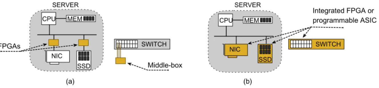
Nonetheless, the benefits of executing application logic close to networking and storage devices are known [17, 40]. New algorithms that take advantage of proximity to the data become viable and provide both performance and power consumption gains. Figure 1(a) illustrates how FPGAs and network “middle-boxes” can create these opportunities.
The lack of programmability in network and storage devices has impacted not only applications. It has also hindered the advancement of these platforms. On the networking side, new protocols emerge that depend heavily on hardware to run at high-speeds. Fixed-function devices, the ones that have their functionality “baked”
Copyright 2020 IEEE. Personal use of this material is permitted. However, permission to reprint/republish this material for advertising or promotional purposes or for creating new collective works for resale or redistribution to servers or lists, or to reuse any copyrighted component of this work in other works must be obtained from the IEEE.
Bulletin of the IEEE Computer Society Technical Committee on Data Engineering
!"# $%$ &'()!* &&+ ,(! !"# $%$ &&+ ,(! &'()!* -"./0 $122345678 (9:4;<=:42>-"./>7< ?<7;<=@@=634>/&(! A=B A6B &%CD%C &%CD%C
Figure 1: Alternative in-network computing and near-storage processing platforms. (a) Using “bump-in-the-wire” FPGAs or network “middle-boxes” to create early application logic sites. (b) Leveraging programmability within the device for application logic.
into the hardware, may need to undergo a full, lengthy development cycle before they can run new protocols. Recently, a solution emerged where a new class of networking devices started supporting programmability (e.g., in programmable switches [6] and “smart” NICs [44]). The protocols these devices run are expressed as software programs.
The need for programmability also emerged on storage platforms recently. SSDs are designed to shield applications from the intricacies of managing flash memory. However, evidence appeared that SSDs often miss the right performance decisions because of the separation between it and the applications [3]. A more modular SSD design, deemed open-channel, was proposed that allows a host (a server), rather than the SSD itself, to make certain low-level decisions. The modules that run on the host are software-based, therefore programmable.
Developers soon realized that the programmability could also be used by applications. It made it possible to inject application code directly into the networking and storage stacks. Figure 1(b) depicts such a scenario. In-network computing and near-storage processing emerged as the disciplines that leverage processing power in the network and storage stacks, respectively, for application purposes.
An application that benefits from INC or NSP contains, by definition, algorithms running in different com-puting elements of a system. These algorithms ought to communicate at high speed. The most commonly used interconnect for such systems has been based on the PCIe bus standard [8]. At this time, the standard is being revised to operate at higher speeds. PCIe is also being extended with mechanisms to support cache coherence protocols to run atop of it [12, 14].
Despite their potential, INC and NSP platforms are not without challenges. INC is a more mature technology with increasingly popular programmable models that shield the developer from the intricacies of the devices. Such programming models, however, are quite different from a general-purpose CPU’s. In contrast, NSP often uses general-purpose processors—but much less powerful ones than server-class CPUs. In both cases, porting algorithms to these platforms requires rethinking the algorithms to fit either a different model or a less-powerful environment.
In this paper, we elaborate on the above challenges and opportunities of adopting INC and NSP as platforms to improve application performance. We summarize the contributions of this paper are as follows:
• We discuss the evolution and recent advancements of INC and NSP platforms; • We present specific computation tasks that can benefit from them;
• We describe the challenges that still remain in order to use INC and NSP as application platforms; • Finally, we present the benefits of adopting the current generation of INC and NSP.
The rest of this paper is structured as follows. We discuss the programmability of the network and storage stacks in more detail in Section 2. We show examples of computing paths that can leverage INC and NSP capabilities in Section 3. We comment on the evolution of the PCIe interconnect and the possibilities it opens
in Section 4. We discuss the challenges and opportunities of adopting INC and NSP platforms in Section 5. We elaborate on how ready for adoption the technologies are in Section 6, before concluding in Section 7.
2 An Abridged History of INC and NSP
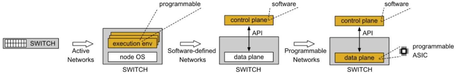
There have been many attempts to conciliate speed and flexibility in networking hardware devices. Figure 2 depicts the main ideas behind the relevant milestones in that context.
!"#$%& '()*+,! -('./(0+102'* )2.2+102'* 34# -('./(0+102'* )2.2+102'* 34# 3-.56*+ 7*.8(/9: :(;.82/* 1/(</2==2>0* 3!#% !(;.82/*?)*;5'*) +7*.8(/9: 4/(</2==2>0* +7*.8(/9: :(;.82/* 1/(</2==2>0* *@*-A.5('+*'6
!"#$%& !"#$%& !"#$%&
Figure 2: Evolution of the network stack towards programmability.
Active Networks, one of the first attempts, proposed a standard architecture for more flexible network de-vices [10]. The goal of the architecture is to enable changes to the device behavior—–typically to implement new protocols—–via the execution of user-driven customization. There are two main components in such a device. First, a node operating system that manages basic IO functionality, including processing, storage, and transmission. Second, multiple Execution Environments (EE) that support the execution of programs containing packet-processing logic. Applications can inject code into the device through an API, which generates special packets for the device to execute. Active networks proved to be very flexible; however, they ran considerably slower than their fixed-function counterparts.
Software-Defined Networks (SDN), a later attempt at a more flexible network, is also centered around a standard device architecture [23]. The main feature of the architecture is the separation of the control plane (policy definition) from the data plane (policy implementation). The control plane would contain information such as routing tables; the data plane would use that information to forward packets without sacrificing speed. An SDN device could adopt a new protocol if the SDN standard recognizes that protocol. Introducing new protocols, however, still required changes in the SDN standard itself and sometimes also on the devices. The main issue was that SDN only supports custom logic on the control plane. Protocols that depended on special per-packet logic need to send these packets to the control plane, which in turn processes them, pushing the results back to the data plane. The additional path cannot sustain line-rate, as one calls the individual port speed of a switch.
In a more recent development, Programmable Dataplanes (also referred to as Programmable Networks) allowed custom logic on the data plane [2]. The cornerstone of this technology is a generation of programmable ASICs (chips) that supports a certain degree of stateful packet processing without compromising speed [6]. This balance is captured by a programming model called Protocol Independent Switch Architecture (PISA) [38]. PISA shields the programmer from various device intricacies and, because it was designed to be protocol-independent, it proved adept at expressing application computations as well. Programmable networks created the conditions for a new generation of applications to push specialized logic into the network, i.e., to perform in-network computing.
We now turn our attention to the evolution of the storage stack. Just as with networks, the idea of near-storage processing is not new, but the driver for altering this stack has been more application-centric than in networking. In the early 2000s, a seminal proposal, called Active Disks, gained traction that aimed at transforming hard drive controllers into data-processing platforms [35]. These controllers often carried a small, general-purpose
processor that was somewhat over-dimensioned for its purpose. Applications could place logic on that processor, and access/modify the data blocks that were streaming in and out of the hard drive. The computing power of these controllers ultimately proved to be underwhelming, and the industry saw little need to improve them.
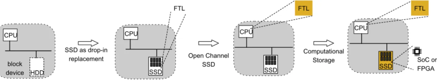
Eventually, SSDs based on NAND-flash displaced hard drives in many applications. Managing flash mem-ory requires considerably more computing power than a magnetic medium, and flash memmem-ory error rates are very high, which requires computational-intensive error correction techniques [9]. Moreover, the industry de-cided that SSDs should be drop-in replacements for hard drives. SSDs execute internally a compatibility layer called Flash Translation Layer (FTL) for that purpose [13]. All these factors turn SSDs into relatively powerful embedded devices.
A proposal soon emerged to leverage SSD controllers for database query processing using smart SSDs [15]. As with active disks, the computing capacity on early devices was not sufficient for most computations in practice [16]. It would take a new generation of devices to accommodate fast database logic [21]. However, the industry focus was more on making devices faster than on making them smarter. Performance wasting was an issue, as the FTL not always makes the best decisions from an application’s point of view. Some efforts emerged that tried to make SSD architectures more open to configurations. Figure 3 captures the essential steps of this effort. !"" #$%&' ()*+&) ,-)./012..)$ 33" 0%4-5626+%.2$ 36%728) 33" 09: ;<= 33" 09: ;<= 3%0/%7 ;9>? ;<= 33" 09: 33"/2@/(7%-A+./ 7)-$2&)4).6 09:
Figure 3: Evolution of the storage stack towards programmability.
Open Channel SSDs appeared from a growing understanding that many of the FTL tasks were better per-formed leveraging application knowledge [3]. In an open-channel SSD, some of the FTL responsibilities are removed from the device. Instead, they run on the host housing the SSD or even inside individual applica-tions [30]. Naturally, these devices expose a lower-layer view of the underlying flash medium.
With more exposure to SSD architectural details, several works emerged to build tooling around these de-vices. These efforts range from frameworks to program SSD controllers [33], to performance measurement tooling [26], to even full SSD rapid prototyping platforms [24]. At the same time, a class of works appeared that deploy application code on SSDs, making them a Computational Storage platform [32, 37, 43]. The common thread in these works is that they increase the existing computing power of the devices by building them on platforms such as a System-on-a-Chip (SoC) or an FPGA. The tooling and the additional computing capacity paved the way for Near-Storage Processing.
One problem that remains open, however, is the lack of a consensus around a programming model. While there are recent proposals in that sense (e.g., in [18]), these models leave many aspects undefined. For instance, they have not addressed how to interface application logic with internal device mechanisms. An application that wishes to influence the IO scheduling policy of a device directly has no means to do so. There is also no consensus on how to shield an application developer from specific aspects of different devices.
3 Alternative Computing Paths
INC and NSP provide alternative sites beyond a CPU where applications can place logic. This fundamentally changes the traditional data movement patterns we see in CPU-centric algorithms, potentially bringing perfor-mance and power savings benefits. We illustrate these possibilities in this section by presenting and discussing
several use cases in large-scale data management. 3.1 In-Network Data Aggregation
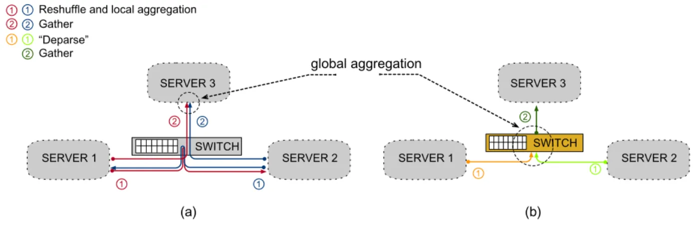
Data aggregation is a very common operation in data management. Aggregation involves grouping data by specific criteria and calculating summaries over each group. A typical example is the GROUP BY clause in SQL. When the data volume is large, the operation can involve several servers, e.g., as in a rack-wide computation. Figure 4(a) illustrates one possible way to solve such a distributed aggregation.
The servers agree on how to partition the data, taking into consideration the grouping key. This divides the work into disjoint, independent tasks. Each server reshuffles its data while performing the aggregation over its assigned partition, as data arrives. Eventually, all the machines send their aggregation results to an elected server, which combines them into a global result. Note that throughout all these interactions, the switch performs data transmissions only. !"#$%& !"#$%& '() '*) !+,-+,./ !+,-+,.0 !+,-+,.1 !+,-+,./ !+,-+,.0 !+,-+,.1 2 3 ,45678894.(:;.9<=(9.(>>?4>(@A<: B(@64? 2 3 2 3 3 2 2 2 2 CD4E(?54F 2 3 3B(@64? >9<*(9.(>>?4>(@A<:
Figure 4: Data aggregation scenario (e.g., SQL GROUP BY). (a) With a “passive” switch, the servers first repartition the data and work on aggregating its assigned partition locally. Then, an elected server gathers all partitions and performs the global aggregation. (b) On an INC platform, an “active” switch can, in typical situations, perform the global aggregation in one step and transmit the results to an elected server. We use a given color to represent each unique data stream in the computation.
In Figure 4(b), we show that using the switch as an active element simplifies the entire computing path [25]. We assume that the switch is programmable and that it can be leveraged to hold an entire aggregation table. The size of such a table is often manageable, as it is proportional to the number of groups involved, rather than the size of the dataset. Note that the servers need not reshuffle the data nor perform an aggregation on a partition. Because programmable switches perform computations at line-speed, the aggregation table on the switch will be completed as soon as the last server finishes transmitting its tuples, and can then be sent immediately to an elected server.
Not all computations are suitable for INC deployment. The important caveats include: (a) the number of steps the switch can execute over each packet is limited; (b) the kind of instructions the switch can perform is also constrained; and (c) programmable network devices adhere to a programming model that imposes a forward logic-style onto algorithm design. Loops and complex branching are strongly discouraged, although possible. In practice, these restrictions reduce the choices of data structures the switch can support. In particular, the aggregation described in Figure 4(b) requires a hash table to be adapted to INC constraints. In this case, the number of collisions can be handled on the switch up to a certain bound. Relaxing this constraint involves using a technique called “overflowing” [25], which allows treating long collision chains outside the switch without a noticeable performance penalty in most cases.
These limitations notwithstanding, a large class of computations can benefit from INC platforms [34]. More-over, processing data on the switch tends to scale well as the number of servers grows in the cluster. The number of switches naturally grows with the number of servers.
3.2 Near-Storage Checkpoint Derivation
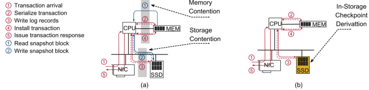
We now describe an opportunity that arises specifically in an in-memory database system. Like most DBMSs, in-memory databases guarantee durability using a persistent transaction log. Because the log can get arbitrarily long, it would be impractical to recover from a crash just by replaying it. Therefore, databases also perform a periodical checkpoint (e.g., by taking a snapshot) of the current memory state and write it to persistent storage, often SSDs. A recovery algorithm can load the snapshot and replay the portion of the log acquired after the checkpoint. In in-memory databases, the log and checkpoint are the only workloads written to disk.
The logging and checkpointing processes compete for both disk and memory bandwidth. Figure 5(a) shows these contention points. The checkpointing process reads the database contents from the main-memory while it is being queried/modified. The checkpointing process also issues write requests to the SSD, which have to be scheduled along with the logging workload. The contention is responsible for the throughput reduction that many systems experience during checkpoints.
!!" #$% &'& ()# * + * + , -. )/0!123456 #7689:2;/1 "63;<411;2/ &6=23>? #2/16/1;2/ !123456? #2/16/1;2/ @4A @BA * + , -. C34/D481;2/?433;<4E !63;4E;F6?134/D481;2/ G3;16?E25?36823HD? )/D14EE?134/D481;2/ * + )DDI6?134/D481;2/?36D:2/D6 G3;16?D/4:D721?BE289 J64H?D/4:D721?BE289 !!" #$% &'& ()# * + , -.
Figure 5: Checkpoint computation scenario. (a) Transaction logging (red) and checkpoint (blue) are two parallel processes. They compete for memory and disk bandwidth. (b) A checkpoint could be derived by processing the transaction log inside an SSD. The solid lines represent data; the dashed ones, control and/or return.
The key observation here is that partial snapshots, which can serve as checkpoints, can be derived from the log stream directly. We believe that such derivations may very well occur inside a smart SSD. We show in Figure 5(b) that once we move that process to the device, the contention points disappear.
Note, however, that the processing power on an SSD is far smaller than that of a general-purpose CPU. We cannot possibly expect to move the same algorithm we used on a CPU into an NSP platform and obtain similar performance results. Creating a checkpoint derivation algorithm for an SSD requires finding snapshot approximations that the device can process at the necessary pace. We comment on Section 5 how specific architectural changes on smart SSDs can make this task easier.
3.3 Low Latency Database Replication
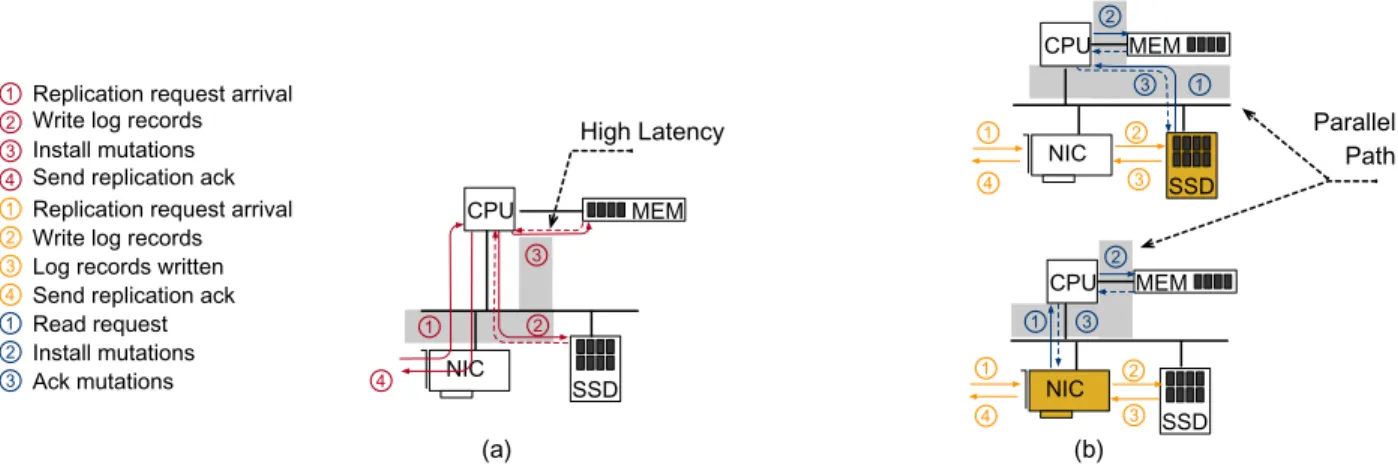
Another code path that can benefit from either INC or NSP is that of a replica node in a database system. On a master node, transactions need to be serialized via a concurrency control algorithm. The latter typically runs on a CPU. The replica node code-path is simpler because the serial order of the transactions was already determined. The CPU takes the modifications coming from the network card and persists them on disk in the same order it received them. Subsequently, it updates its data structures and sends a notification to the master node that it accepted the transaction. Figure 6(a) depicts such an interaction.
!!" #$% &'& ()# * + , -* + ./01234567892 !!" #$% &'& ()# * + , * , -* + , -:6;</845/=72>6?@6A524>>/B4< C>/562<=02>68=>DA2 )7A54<<2E@545/=7A * + , :64D2>6?@6A5 )7A54<<2E@545/=7A F8G2E@545/=7A !67D2>6;</845/=7248G * + , -:6;</845/=72>6?@6A524>>/B4< C>/562<=02>68=>DA2 3=02>68=>DA2H>/55672 !67D2>6;</845/=7248G $4>4<<6< $451 !!" #$% &'& ()# * + , -, + I4J IKJ
Figure 6: Database replica node scenario. (a) Each transaction log entry is first persisted in storage and then applied to memory, as the CPU coordinates the replication. (b) If an “active” NIC or SSD coordinates the process, the persistence and memory update paths can proceed in parallel.
Note that the replica code path incurs in latency. The master node may be withholding the original transaction until the replication path is completed. We can optimize this code path in at least two ways. Using NSP, the NIC would send the modification stream directly to a smart SSD. In turn, the SSD could be programmed to coordinate the interaction instead of the CPU. The SSD would notify the NIC after it persisted the changes, reducing the latency. It would also, in parallel, allow the CPU to read (and perform) the modifications. An alternative path exists where the NIC itself would perform the coordination. Figure 6(b) shows both cases. This scenario involves having the NIC and the SSD communicate without any CPU intervention. This type of communication is called peer-to-peer DMA [8] and it has been used in other contexts before, such as direct access to a remote disk (e.g., NVMe-over-Fabrics [19]).
4 Upcoming Interconnects
INC and NSP platforms rely on an interconnect to communicate with other computing elements in a system. PCIe has been the de facto interconnect for quite a while [8]. PCIe is a point-to-point bus with a variable number of lanes dedicated to devices. Each lane can transfer close to 1GB/s on the current standard version, Gen 3. Cards attached to the bus can use 1×, 2×, 4×, 8×, or 16× lanes to achieve a theoretical maximum of 16 GB/s bidirectional bandwidth.
Newer devices are creating the need for faster speeds. For instance, the standard NIC port speeds are about to go from 100 Gb/s to 400 Gb/s, which a single Gen 3 PCIe slot can no longer support. The PCIe standard had moved to 2 GB/s lanes on Gen 4. The following iteration of the standard, Gen 5, brings 4 GB/s lanes with a theoretical bi-directional bandwidth of 64GB/s for 16× device.
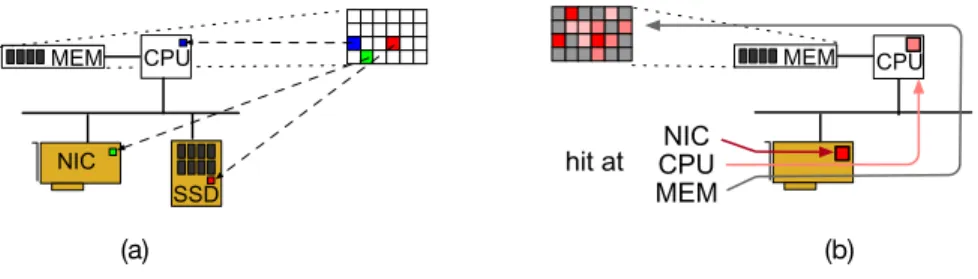
There is another compelling feature that new versions of PCIe buses will bring: cache coherence. This feature allows computing elements to negotiate who may be caching a given portion of memory at any given time. It also determines who has the license to write to that memory address. Coordinating access to single memory address allows all the computing elements to share a single view of memory, as Figure 7(a) shows. There are two flavors of coherency: one in which the CPU has a prominent role in controlling the memory, called asymmetric, and one in which all computing elements play a similar role, called symmetric.
At the time of writing, there are four upcoming interconnects offering both high speed and coherence: CAPI [39], CCIX [12], CXL [14] and Gen-Z [22]. CCIX and Gen-Z support symmetric coherence, unlike CAPI or CXL, which support asymmetric coherence. CAPI is a competing standard to PCIe. CCIX and CXL use only
!!" #$% &'& ()# #$% &'& (a) (b) *+,-.,-()# #$% !"!
Figure 7: Cache coherency scenarios: (a) a NIC and an SSD may be responsible for writing to specific addresses in memory that can be read by other elements, and (b) a NIC can be responsible for caching (and writing to) very hot pages while leaving the CPU responsible for less accessed pages.
PCIe, while Gen-Z can use ethernet as well as PCIe. The range of PCIe is short enough to work only within the confines of a chassis, while ethernet allow to connect across chassis. This opens up the possibility of CCIX or CXL being applied simultaneously with Gen-Z to form coherence domains that cross server boundaries.
Cache coherency allows for new INC and NSP design use cases. For instance, one may extend the caching hierarchy beyond the CPU. Figure 7(b) illustrates this possibility. Some distributed applications may cache hot data items in the NIC [41]. With coherence, the NIC can also request write access to such an item and update it. Any other computing element that requests to cache that address would then see the updates.
5 Challenges and Opportunities
We mentioned above some immediate difficulties that arise when deploying current generation INC and NSP platforms. In this section, we elaborate on further challenges and opportunities that we believe would unlock more of the potential of these platforms.
In-Network Stateful Computations. Data management primarily involves stateful computations, i.e., algo-rithms that access a result from a previous iteration and generate a new result at the next one. The aggregation operation discussed in Section 3.1 is one such algorithm. Maintaining state in-network, particularly in switches, is currently very challenging. Programmable switches rely on high-speed memories that, for cost reasons, are present in limited amounts. Moreover, switches have a very strict “allowance” of how many instructions they can execute per packet and what those instructions can do. These restrictions make maintaining data structures other than a hash table on a switch possible but difficult. Even some common operations on hash tables, such as collision management, require some adapting, as we discussed above.
We miss a computing model that can relax those restrictions to a certain extent while still keeping the ability to run logic at line-speed. Supporting such a model would most likely require introducing new hardware onto programmable switches. We believe such a model is possible, but the field of in-network computing is still new. There is not yet a clear list of missing operations from applications beyond networking protocols on which to base new switch hardware capabilities.
SSD-Application Interface. A regular SSD makes several decisions such as IO scheduling and page mapping based solely on observing the stream of IO commands it receives [28]. When application logic executes inside the device, it becomes an additional stream of IO commands. The internal and external streams would likely compete with one another. A straightforward way to manage the new internal streams is to pretend they came from outside and to proceed as usual.
An alternative way would be to allow the application logic and the device to interact. Consider again the checkpoint derivation scenario we describe in Section 3.2. It generates new IO requests at a given pace. Depend-ing on the current load on the SSD, the checkpoint stream can be too fast or too slow for the device to handle.
Ideally, we want a means for the device and the application logic to negotiate that pace. There is an opportunity here to establish a communication model that supports this kind of interaction.
SSD Channel Architecture. An SSD’s bandwidth and capacity are a result of combining many relatively limited NAND flash packages (chips) [27]. A typical arrangement is to group the packages in disjoint sets called channels. There are anywhere between 8 to 32 channels in a typical SSD. This arrangement has proved adequate when data pages are transferred in and out of the device.
The introduction of application logic into an SSD, however, can cause data pages to be moved across pack-ages—possibly between channels. For instance, we describe in Section 3.2 how an NSP process can read pages from a transaction log and write them, after some manipulation, as pages of a checkpoint. In a traditional SSD architecture, this pattern would consume bandwidth from both the origin and the destination channels. We be-lieve that there may be other package interconnect architectures beyond channels that are more suited to the data movements above. To the best of our knowledge, there has been no study about interconnects that involve architectures other than fixed channels.
Code-Variant Generation and Selection. INC and NSP platforms introduce additional hardware heterogeneity to computing platforms. An algorithm implementation that works well on a given switch may not work on a different one, due to architectural differences. The generation and selection of variant implementations is a known problem; it appeared before in domains such as GPUs [36].
To complicate matters, some algorithms are flexible enough to be deployed either on a NIC or on the switch to which it connects. The selection of the most appropriate platform constitutes an optimization step that compounds to the variant selection problem above. Currently, the programmer is responsible for making such choices. There is an opportunity for creating higher-level tooling that would aid in these decisions. Runtime Resource Management. In a regular setting, the operating system mediates every single network and storage IO between applications and devices. The OS does so by interposing itself between the two. What, then, should be the role of the OS when a portion of the applications reside inside the device?
One potential solution is to accept that applications may want to access a device directly, without mediation. Such is the premise of Arrakis [31], which tricks an application into interacting with virtual versions of the devices, and redesigns the kernel to provide the expected protections under such assumptions.
6 Discussion
Notwithstanding the challenges and opportunities described in the previous section, INC and NSP platforms are a reality. The question arises as to whether they are ready for adoption. In this section, we break this question into a list of sub-questions and answer each one in turn.
Are there diverse offerings of INC and NSP platforms? INC can be realized by many different hardware targets, both on switches and NICs. In terms of programmable switches, there are at least three silicon man-ufacturers producing programmable ASICs: Barefoot (Intel) Tofino [1], Broadcom Trident 4 [5], and Cavium (Marvel) Xpliant [11]. Together, these chips appear in several commercial offerings from companies such as Cisco and Arista. SmartNICs are also widely available, ranging from FPGA-centric accelerators such as Xilinx Alveo [42] to more software-oriented platforms such as Netronome [29]. The offering for programming lan-guages and abstractions is also diverse. A prevalent language is P4 [7], but there are variations such as NPL [4] and even C libraries in some cases [29].
NSP is also a rich environment with many prototyping and commercial platforms available. For instance, SSDs are starting to emerge that introduce application specializations. Samsung has recently announced the KV-SSD, which incorporates Key Value store logic within its firmware [20]. One issue with such offerings is that they add application functionality but do not expose programmability. The interested reader should look
at [33] for an extensive list of specialized SSD and NSP-platforms available at the time of writing.
What are the advantages of INC and NSP compared to “CPU-centric” alternatives? While there is no study yet of an exacale platform that resorts to both INC and NSP, the expected benefits are a combination of increased performance, lower energy expenditure, and lower CPU utilization. There a numerous works that provide partial results.
For INC, data manipulations such as the one described in Section 3.1 were studied before [25]. We can expect to see the performance of many typical queries improve by a factor of 2× by using programmable switches at moderate network speeds. The power consumption in these switches is estimated to be only 12.4% higher than their fixed-function counterparts, and, anecdotally, the switches cost about the same. The operations-per-Watt ratio on some INC platforms such as smartNICs was also studied before [41]. For instance, a variant of the caching scenario we discussed in Section 4 reports a 17× better power utilization as compared to a regular CPU. NSP platforms deliver similar benefits. According to [21], the performance of scans and joins can see per-formance improvements between 5× and 47×, the cost of equipping an SSD to support near-storage processing is less than 1% of its total cost, and the energy-efficiency compared to performing those operations on a CPU can be up to 45× better.
Are there standards in place to guarantee the portability and longevity of the solutions? There is a big difference from a standardization point of view between INC and NSP technologies. As mentioned above, INC has broadly embraced P4 as a programming language. The latest edition of the language, P416, allows different target platforms to express their capabilities. A compiler can generate specific code from a unique source to different, maybe even disparate, devices. These feature makes the language flexible enough to work on future devices, which can only help its adoption.
In contrast, there is not yet a consensus on how computational storage should be programmed. We even miss a standard around what an open-channel SSD should be, which would arguably be a necessary step.
7 Conclusion
In this paper, we reviewed how the evolution of the network and storage stacks have unlocked their computing power. Applications can not only request services from these stacks, but also embed logic into them. We showed that with a careful redesign, algorithms running on INC or NSP platforms could present a reduced amount of data movement, lower CPU utilization, less energy consumption, or a combination of these.
We also discussed several challenges that INC and NSP still face. Despite these limitations, we commented on a current generation of INC- and NSP-enabled devices that are available off-the-shelf. We believe that the emergence of the network and storage stacks as computing elements creates promising ways to scale typical data management computations.
Acknowledgments. This project has received funding from the European Research Council (ERC) under the European Unions Horizon 2020 research and innovation programme (grant agreement 683253/GraphInt).
References
[1] Barefoot Tofino and Tofino 2 Switches. https://www.barefootnetworks.com/products/brief-tofino-2/.
[2] R. Bifulco, and G. R´etv´ari. A Survey on the Programmable Data Plane: Abstractions, Architectures, and Open Problems. HPSR, June, 2018.
[3] M. Bjøling, J. Gonz´alez, and P. Bonnet. Lightnvm: The Linux Open-Channel SSD Subsystem FAST, February, 2017. [4] Broadcom NPL. Network Programming Language. https://nplang.org/.
[5] Broadcom. Broadcom Trident 4. https://www.broadcom.com/products/ethernet-connectivity/switching/strataxgs/bcm56880-series.
[6] P. Bosshart, G. Gibb, H.-S. Kim, G. Varghese, N. McKeown, M. Izzard, F. Mujica, and M. Horowitz. Forwarding Metamorphosis: Fast Programmable Match-Action Processing in Hardware for SDN. SIGCOMM CCR, 43(4):99– 110, 2013.
[7] P. Bosshart., D. Daly, G. Gibb, M. Izzard, N. McKeown, J. Rexford, C. Schlesinger, D. Talayco, A. Vahdat, G. Vargh-ese, and D. Walker. P4: Programming protocol-independent packet processors. ACM SIGCOMM CCR, 44(3):87–95, 2014.
[8] R. Budruk, D. Anderson, and E. Solari. PCI Express System Architecture. Pearson Education, 2003.
[9] Y. Cai, S. Ghhose, E.F. Haratsch, Y. Luo, and O. Mutlu. Error Characterization, Mitigation, and Recovery in Flash-Memory-Based Solid-State Drives. Proc. of the IEEE, 105(9), 1666–1704, 2017.
[10] K.L. Calvert, S. Bhattacharjee, E. Zegura, and J. Sterbenz. Directions in Active Networks. IEEE Comm. Magazine, 36(10):72–78, 1998.
[11] Cavium. XPliant Ethernet Switch Product Family. www.cavium.com/XPliant-Ethernet-Switch-Product-Family.html [12] CCIX Consortium. An Introduction to CCIX. White Paper,
https://www.ccixconsortium.com/wp-content/uploads/2019/11/CCIX-White-Paper-Rev111219.pdf
[13] T.-S. Chung, D.-J. Park, S. Park, D.-H. Lee, S.-W. Lee, and H.-J. Song. A Survey of Flash Translation Layer. J. of Syst. Archit., 55(5–6):332–343, 2009.
[14] D.D. Sharma. An Introduction to Compute Express Link. White Paper,
https://docs.wixstatic.com/ugd/0c1418 d9878707bbb7427786b70c3c91d5fbd1.pdf.
[15] J. Do, Y.S. Kee, J.M. Pzatel, C. Park, K. Park, and D.J. DeWitt. Query Processing on Smart SSDs: Opportunities and Challenges. SIGMOD, June, 2013.
[16] J. Do, S. Sengupta, and S. Swanson. Programmable Solid-State Storage in Future Could Datacenters. CACM, 62(6):54–62, 2019.
[17] J. Fang, Y.T.B. Mulder, J. Hidders, J. Lee, and H.P. Hofstee. In-Memory Database Acceleration on FPGAs: A Survey. VLDB Journal, October, 2019.
[18] B. Gu, A.S. Yoon, D.H. Bae, I. Jo, J. Lee, and J. Yoon. Biscuit: A Framework for Near-Data Processing of Big Data Workloads. SIGARCH Comp. Arch. News, 44(3):153–165.
[19] Z. Guz, H. Li, A. Shayesteh, and V. Balakrishnan. Performance Characterization of NVMe-over-Fabrics Storage Disaggregation. ACM Trans. on Storage, 14(4):1553–3077, 2018.
[20] Y.-S. Ki. Key Value SSD Explained – Concept, Device, System, and Standard. SNIA SDC, September, 2017. [21] S. Kim, H. Oh, C. Park, S. Cho, S.-W. Lee, and B. Moon. In-Storage Processing of Database Scans and Joins. Inf.
Sci., 327(C):183–200, 2016.
[22] P. Knebel, D. Berkram, A. Davis, D. Emmot, P. Faraboschi, and G. Gostin. Gen-Z Chipset for Exascale Fabrics. HotChips, August, 2019.
[23] D. Kreutz, F.M.V. Ramos, P.E. Ver´ıssimo, C.E. Rothenberg, S. Azodolmolky, and S. Uhlig. Software-Defined Net-working: A Comprehensive Survey. Proc. of the IEEE, 103(1):14–76, 2015.
[24] J. Kwak, S. Lee, K. Park, J. Jeong, and Y.H. Song. Cosmos+ OpenSSD: Rapid Prototype for Flash Storage Systems. ACM Trans. on Storage, to appear.
[25] A. Lerner, R. Russein, and P. Cudr´e-Mauroux. The Case for Network Accelerated Query Processing. CIDR, January, 2019.
[26] A. Lerner, J. Kwak, S. Lee, K. Park, Y.H. Song, and P. Cudr´e-Mauroux. It Takes Two: Instrumenting the Interaction between In-Memory Databases and Solid-State Drives. CIDR, January, 2020.
[28] E.H. Nam, B. S. J. Kim, H. Eom, and S. L. Min. Ozone (O3): An Out-of-Order Flash Memory Controller Architec-ture. IEEE Transactions on Computers, 60(5):653–666, 2011.
[29] Netronome. Agilio CX SmartNICs. https://www.netronome.com/products/agilio-cx/
[30] J. Ouyang, S. Lin, S. Jiang, Z. Hou, Y. Wang, and Y. Wang. SDF: Software-Defined Flash for Web-Scale Internet Storage Systems. ASPLOS, 2014.
[31] S. Peter, J. Li, I. Zhang, D.R.K. Ports, D. Woos, A. Krishnamurthy, T. Anderson, and T. Roscoe. Arrakis: The Operating System Is the Control Plane. ACM TOCS, 33(4), 2015.
[32] I.L. Picoli, P. Bonnet, and P. T¨oz¨un. LSM Management on Computational Storage. DaMoN, July, 2019.
[33] I.L. Picoli, N. Hedam, P. Bonnet, and P. T¨oz¨un. Open-Channel SSD (What Is It Good For). CIDR, January, 2020 [34] D.R.K. Ports, and J. Nelson. When Should The Network Be The Computer. HotOS, May, 2019.
[35] E. Riedel, C. Faloutsos, G.A. Gibson, and D. Nagle. Active Disks for Large-Scale Data Processing. IEEE Computer, 34(6):68–74, 2001.
[36] V. Rosenfeld, M. Heimel, C. Viebig, and V. Markl. The Operator Variant Selection Problem on Hetergoneous Hardware. ADMS, August, 2015.
[37] Z. Ruan, T. He, and J. Cong. INSIDER: Designing In-Storage Computing System for Emerging High-Performance Drive. Usenix ATC, July, 2019.
[38] A. Sivaraman, A. Cheung, M. Budiu, C. Kim, M. Alizadeh, H. Balakrishnan, G. Varghese, N. McKeown, and S. Licking. Packet transactions: High-level programming for line-rate switches. SIGCOMM, August, 2016.
[39] J. Stuecheli, B. Blaner, C.R. Johns, and M.S. Siegel. CAPI: A Coherent Accelerator Processor Interface. IBM Journal of Research and Development, 59(1):1–7, 2015.
[40] J. Teubner, and L. Woods. Data Processing on FPGAs. Morgan & Claypool Publishers, 2013.
[41] Y. Tokusashi, H. Matsutani, and N. Zilberman. LaKe: The Power of In-Network Computing. ReConFig, December, 2018.
[42] Xilinx. ALVEO Adaptable Accelerator Cards for Data Center Workloads.
https://www.xilinx.com/content/xilinx/en/products/boards-and-kits/alveo.html
[43] L. Woods, Z. Istv´an, and G. Alonso. Ibex: An Inteligent Storage Engine with Support for Advanced SQL Offloading. Proc. of the VLDB, 7(11):963–974.
[44] N. Zilberman, Y. Audzevich, G.A. Covington, and A.W. Moore. NetFPGA SUME: Towards 100 Gbps as Research Commodity. IEEE Micro, 34(5):32–41, 2014.