Design, Implementation, and Evaluation of
High-Efficiency High-Power Radio-Frequency
Inductors
by
Roderick S. Bayliss III
S.B., Massachusetts Institute of Technology (2020)
Submitted to the Department of Electrical Engineering and Computer
Science
in partial fulfillment of the requirements for the degree of
Master of Engineering in Electrical Engineering and Computer Science
at the
MASSACHUSETTS INSTITUTE OF TECHNOLOGY
February 2021
© Massachusetts Institute of Technology 2021. All rights reserved.
Author . . . .
Department of Electrical Engineering and Computer Science
January 15, 2021
Certified by . . . .
David J. Perreault
Professor of Electrical Engineering and Computer Science
Thesis Supervisor
Accepted by . . . .
Katrina LaCurts
Chair, Master of Engineering Thesis Committee
Design, Implementation, and Evaluation of High-Efficiency
High-Power Radio-Frequency Inductors
by
Roderick S. Bayliss III
Submitted to the Department of Electrical Engineering and Computer Science on January 15, 2021, in partial fulfillment of the
requirements for the degree of
Master of Engineering in Electrical Engineering and Computer Science
Abstract
Radio-Frequency (RF) power inductors are critical to many application spaces such as communications, RF food processing, heating, and plasma generation for semicon-ductor processing. Insemicon-ductors for high frequency and high power (e.g., tens of MHz and hundreds of watts and above) have traditionally been implemented as air-core solenoids to avoid high-frequency core loss. These designs have more turns than magnetic-core inductors and thus high copper loss; their high loss and large size are both major contributors to the overall system efficiency and size.
One contribution of this thesis is a magnetic-core inductor design approach that leverages NiZn ferrites with low loss at RF, distributed gaps and field balancing to achieve improved performance at tens of MHz and at hundreds of watts and above. This approach is demonstrated in a 13.56 MHz, 580 nH, 80 𝐴𝑝𝑘magnetic-core inductor
design that achieves a quality factor of > 1100, a significant improvement over 𝑄∼600 achieved by conventional air-core inductors of similar volume and power rating.
This thesis additionally describes the difficulties in experimentally measuring in-ductor quality factors with very high current and very low loss at very high frequency. Several measurement techniques are proposed and evaluated to enable consistent mea-surement of inductor resistance at these operating points.
Finally, these design techniques are extended to an inductor design which achieves “self-shielding” in which the magnetic field generated by the element is wholly con-tained within the physical volume of the structure rather than extending into space as a conventional air-core inductor would. This development enables significant re-ductions of system enclosure volume and improvements in overall system efficiency.
Thesis Supervisor: David J. Perreault
Acknowledgments
I’ve been very blessed with the opportunity to study at MIT and work with the power electronics group. Tony, Mohammad, Jessica, Mike, Ben Cary, John Zhang, Alex
Jurkov, Anas, Yiou, Alex Hanson, and Rachel Yang have been the most amazing of friends. Thank y’all for always listening to my complaints about RF voodoo and being
incredibly supportive. You have inspired me to pursue a career in power electronics and for that I will be forever grateful.
I’d also like to thank MIT Motorsports for dealing with my foolish design mistakes (including but not limited to blowing up a very expensive inverter) and strengthening
my practical electrical engineering skills. I will never forget the long nights spent in shop working to finish the car and having fun while doing it. Elijah, Suzy, Maxwell,
Fawaaz, Stefan, Dani, and Becca, thank you especially for being such amazing friends! I would like to thank Fair-rite and MKS for sponsoring this work. Fair-rite both
provided and manufactured the core pieces used in the prototype inductor and MKS provided helpful RF insight and equipment.
My fraternity brothers at Nu Delta are some of the closest friends I’ll ever have. So many fun adventures and late nights and unforgettable memories. I’d like to
especially thank Kebar, Johan, and Yaateh.
I literally wouldn’t be here today without my parents! My entire family has
showered me with love and supported me along this crazy adventure. Mom and dad, pops, uncle, Ben, Reese, auntie Yvonne, Mr. and Mrs. Paseman, Raymond, Sabrina,
Andrew, Stephanie, and auntie Tamara, thank you!
Thank you to all the professors that have guided me along this path.
Char-lie, Dave, and Heidi especially have been nothing but kind, nurturing, sweet, and thoughtful. I cannot overstate how important they were to my growth as an
electri-cal engineer and human.
Finally, I don’t think I’d be where I am today without Katherine Paseman. She
helped guide me towards electrical engineering and has been so supportive and kind. I love you!
Contents
1 Introduction 15
2 Magnetics Materials Characterization 17
2.1 Performance Factor . . . 18
2.2 Test Fixture . . . 19
2.3 Results . . . 20
2.3.1 Example Core Loss Data . . . 20
2.3.2 Performance Factor Graphs . . . 21
3 Proposed High Power RF Inductor Structure and Design 23 3.1 Introduction . . . 23
3.2 RF Distributed Gap Dumbbell Inductor Design . . . 24
3.2.1 Design Overview . . . 24
3.2.2 Field Balancing and Quasi-Distributed Gaps for Improved Per-formance . . . 25
3.2.3 Optimum Aspect Ratio . . . 27
3.2.4 End Cap Height . . . 28
3.2.5 Wire Size and Capacitance . . . 29
3.2.6 Loss Distribution . . . 30
3.3 Conclusion . . . 31
4 Example 580 nH Inductor Design and Construction 33 4.1 Simulation Results . . . 33
5 Quality Factor Measurement Test Fixture 39
5.1 Motivation . . . 39
5.2 Transformer-Based Test Fixture Design . . . 41
5.2.1 Tuning Requirements . . . 44
5.2.2 Transformer Power Handling . . . 45
5.3 Local Rectification/RF Detection . . . 47
5.3.1 Earth Abnormalities . . . 47
5.3.2 Voltage Doubler RF Probe . . . 49
5.4 Air-Core Comparison . . . 52
5.4.1 Inductor Effective Volume . . . 53
5.4.2 Q Spoiling . . . 53
5.5 Results . . . 53
5.6 Sources of Discrepancy . . . 54
6 Self-Shielded Inductor Structure and Design Guidelines 57 6.1 Problem Motivation . . . 57
6.2 Self-Shielded Structure . . . 58
6.2.1 Scripting and Constraints . . . 59
6.3 Results . . . 62
6.3.1 Distributed Gap Turn Spacing . . . 64
6.4 Future work . . . 64
6.4.1 Thermal Limitations . . . 64
6.4.2 End Turn Effects . . . 65
6.4.3 Mechanical Design . . . 67
7 Conclusion 69 7.1 Key Takeaways . . . 69
7.2 Future Work . . . 70
B High Power Inductor Python Script 83
C Shielded Inductor Script 87
D Capacitor Divider PCB 91
E Voltage Doubler PCB 97
F Ferrite Discs CAD Drawings 103
List of Figures
2-1 Magnetic materials loss measurement fixture schematic. . . 19
2-2 Measured core loss data for Hitachi Metals’ ML91S ferrite material. . 20
2-3 Compiled Performance Factor Graphs . . . 22
3-1 CAD model of the RF distributed gap inductor. . . 25
3-2 Magnetic circuit model for the “dumbbell” inductor . . . 26
3-3 ANSYS FEA simulation illustrating the current crowding phenomenon 26 3-4 Quality factor vs. Aspect Ratio . . . 28
3-5 End Cap Height Sweep . . . 29
3-6 Wire Radius Sweep . . . 30
4-1 CAD model of the RF distributed gap inductor. . . 34
4-2 Magnetic Flux Lines of Proposed Inductor . . . 35
4-3 Current Distribution of Proposed Inductor . . . 36
4-4 Copper Coil Former Fixture . . . 37
5-1 Capacitor Voltage Divider Schematic . . . 42
5-2 Simplified Inductor Quality Factor Measurement Fixture Schematic . 43 5-3 Inductor quality factor validation test fixture with prototype inductor. 43 5-4 Example Input Impedance . . . 45
5-5 Inductor Quality Factor Measurement Fixture Schematic Including Parasitics. . . 46
5-6 Birds’ Eye View of Transformer Coupled Resonant Tank Test Fixture. 46 5-7 “Ground to Ground” Probe . . . 48
5-9 Voltage Doubler RF Probe Schematic . . . 49
5-10 Example Voltage Doubler RF Probe and Capacitor Divider Calibration 50 5-11 Voltage Doubler RF Probe Calibration Fixture . . . 51
5-12 Voltage Doubler RF Probe Calibration Fixture Schematic . . . 51
5-13 Measured and Simulated Inductor Performance at 13.56 MHz. . . . . 54
5-14 Thermal Images of Inductor Running at Nearly Full Load Current. . 55
5-15 Inductor Model Including Parasitic Parallel Capacitance . . . 55
6-1 Schematic Polar Cutaway of Self-Shielded Inductor . . . 58
6-2 Self-Shielded Inductor Magnetic Circuit Model . . . 60
6-3 3-D View of Optimal Self-shielded Inductor . . . 62
6-4 Copper Loss By Turn, Sensitivity to z-Position in Window . . . 66
6-5 Schematic Polar Cutaway of Self-Shielded Inductor with Ungapped Ferrite Added to the Window . . . 67
6-6 Copper Loss By Turn, Sensitivity to z-Position in Window, Adding Ungapped Ferrite in Window . . . 68
F-1 CAD Drawing of Ferrite End Cap. . . 104
F-2 CAD Drawing of Ferrite Center Disc. . . 105
G-1 CAD Drawing of Top Capacitor Plate. . . 108
List of Tables
2.1 Magnetic Materials Component List . . . 20
4.1 Geometry of the Proposed Inductor . . . 34
5.1 Voltage Doubler Part Numbers . . . 51
6.1 Comparison Between ANSYS and MATLAB Predictions of Self-Shielded Inductor Structure . . . 63
Chapter 1
Introduction
Typically, magnetic components dominate the size and loss in power electronics. Due to magnetics fundamentals, these components perform worse as they’re made smaller
presenting an unfortunate trade-off between power handling capability and size [12]. Given the necessity of magnetics within many power electronics designs, designers are
placed into a tough corner of fighting strict system requirements and physical limits.
An important subspace of the power field that is a focus in this research is radio
frequency (RF) power electronics. RF is a very wide field encompassing historic challenges like telecommunications and emerging spaces like high power wireless power
transfer and plasma etching. Magnetics designers within this space are again faced with physical limitations that severely hamper their ability to innovate and succeed.
First, skin effect (a phenomenon that reduces the effective conduction area of a wire at AC) and proximity effect (in which fields generated by the inductor current impinge on
other conductors inducing eddy currents and loss) become increasingly exacerbated as frequencies are pushed higher into the RF regime. Second, magnetic materials
(often used to increase inductance or reduce fringing magnetic fields) often exhibit a loss characteristic that increases rapidly with frequency (i.e. 𝑃core ∝ 𝐾𝑓𝛼). Given these physical limitations (in addition to other limitations described later), designing efficient power inductors is a difficult task.
This thesis aims to develop techniques that enable vastly improved RF power in-ductors by leveraging advances in magnetic materials and innovative design
method-Chapter 2 prevents the investigation and characterization of several magnetic materials. Core loss can be a significant limiter of a design’s success especially at
higher frequencies where traditional MnZn ferrites fall flat. Through characterization of new materials such as NiZn ferrites, more efficient, higher frequency magnetic
elements can be produced, opening new design spaces (such as the use of magnetic materials in power magnetics at RF) that were previously closed.
Chapter 3 explores the design techniques and methodologies required to design high power, high frequency, magnetic-core inductors and presents a structure that
utilizes these materials to achieve high performing inductors. Through a combination of magnetic field shaping and quasi-distributed gaps, conductor loss is significantly
reduced compared to conventional air-core designs, yielding inductors with extremely high quality factors.
Chapter 4 presents an example RF inductor design utilizing the structure and design guidelines in chapter 3 yielding a modeled quality factor (Q) 1 of ≈1700 and
a measured quality factor of >1100.
Chapter 5 presents the measurement techniques required to validate this quality
factor. Accurately measuring the mΩ of resistance at a drive current of 80 𝐴pk and 13.56 MHz is no small task. The transformer-coupled resonant tank presented in this
chapter achieves the fundamental requirements of both the production of 80 𝐴pk RF current and utilizing only simple voltage measurements.
Chapter 6 extends the design techniques developed in chapter 3 to a fully “self-shielded” structure in which no magnetic flux exists outside the physical volume of
the structure. Using first principles loss and magnetics modeling and a brute force search, an optimized inductor design using this structure is presented and simulated.
1This thesis uses the following definition of inductor quality factor: 𝑄 = 𝜔𝐿
𝑅ESR, where 𝑅ESR is
the equivalent series resistance of the inductor at the frequency of interest. Note that this definition provides a value that is equal to 2𝜋(peak energy stored)/(energy dissipated in a cycle) for a sinusoidal drive at the frequency of interest.
Chapter 2
Magnetics Materials
Characterization
This chapter reviews a technique to accurately characterize the loss of magnetic
ma-terials in order to assess their potential for use in new power electronics’ applications. It also describes a test fixture used for measuring loss, and presents representative
data from these measurements. Magnetic materials such as ferrite or steel are ben-eficial in many designs as they typically provide non-zero relative permeability 𝜇𝑟,
enabling larger inductance per volume and greater design flexibility. However, these benefits do not come without the penalty of core loss. When magnetic materials are
subjected to a time-varying magnetic flux, they generate heat. Today, this loss is very hard to model and must be empirically measured to predict a design’s performance.
This places designers in a conundrum as manufacturer’s data at operating points of interest may not be reliable or even exist, and these losses are typically non-linear
requiring accurate measurement at a large-signal drive level.
In order to accurately measure the core losses in various magnetic materials, the technique developed in [4] was used. Through this technique, schematically shown
in Fig. 2-1, the device under test (DUT) inductor is resonated with a very low loss capacitor. By measuring the voltage across the capacitor (labeled 𝑣out) and the
voltage input to the tank (labeled 𝑣in), the quality factor and resistance of the inductor (assuming the resistance of the capacitor and external resistances are negligible) can
𝑣out 𝑣in = 1 1 − 𝜔2𝐶 𝑚𝐿𝑚+ (𝑗𝜔𝐶𝑚)(𝑅𝑐𝑢+ 𝑅core) (2.1) At resonance: ⃒ ⃒ ⃒ ⃒ 𝑣out 𝑣in ⃒ ⃒ ⃒ ⃒= (𝜔𝐶𝑚)−1 𝑅𝑐𝑢+ 𝑅core (2.2) 𝑅𝑐𝑢+ 𝑅core= 𝑉in,pk 𝑉out,pk 1 𝜔𝐶𝑚 (2.3) 𝑅core= 𝜔𝐿𝑉in,pk 𝑉out,pk − 𝑅𝑐𝑢 (2.4)
If the resistance of the wire used to wind the inductor (𝑅cu) and the resistance of
the capacitor (𝑅𝑐) are small compared to the equivalent core loss resistance (𝑅core), the total resistance of the tank is approximately 𝑅core.1 A 50 Ω : 3 Ω transmission
line transformer (PN AVTECH AVX-M4) was used to boost the low impedance of the series resonance to ≈ 50 Ω in order to extract pure, high power tones from the
power amplifier. If the power amplifier is loaded with a resistance too far from 50 Ω, it is unable to produce the high-power, single frequency sinusoids requested from it.
Finally, resonance is detected when the input and output voltage waveforms are 90∘ out of phase (with the input voltage leading). By adjusting the resonant capacitance
and slightly deviating the frequency input to the tank from the nominal, desired frequency, resonance can be reached and core loss measurements obtained.
2.1
Performance Factor
In order to easily compare different materials, magnetic material performance factor was used as a figure of merit [8],[6],[11]. Conventional performance factor is defined
by: ℱ = ^𝐵𝑓 where 𝑓 is the frequency of interest and ^𝐵 is the peak flux density that
a material has some specified core loss density (in this case 500 mW/cm3). Material
performance factor can be directly related to the power handling capability of an
1If non-negligible, 𝑅
cu can be approximated and 𝑅𝑐 measured under small-signal conditions or
RF PA 50 Ω 50 Ω : 3 Ω Trans. Line Transformer 𝐿𝑚 𝑅𝑐𝑢 𝑅core 𝐶𝑚 𝑅𝑐 + − 𝑣in + − 𝑣out
Figure 2-1: Magnetic materials loss measurement fixture schematic. The DUT in-ductor 𝐿𝑚 is resonated with a low-loss capacitor 𝐶𝑚. By measuring the ratio of
𝑣out : 𝑣in, the quality factor of the resonant tank can be calculated and the core loss extracted.The transmission line transformer used was of type AVTECH AVX-M4.
inductor or transformer using that material at a given volume [9]. Materials that can handle higher flux densities at higher frequencies for constant power loss are thus
“better” than other materials, allowing designers to quickly pick the best materials for their desired operation frequency. However, this performance factor metric does
not account for variations in winding loss with frequency, and thus overestimates the achievable performance of a magnetic component at frequencies where one is
skin-depth limited and cannot resolve this through use of litz wire or other methods. In order to capture the effect of skin effect limiting conduction area at higher frequencies,
the modified performance factor ℱ3 4 = ^𝐵𝑓
3
4 was introduced in [6], and is also utilized
here.2
2.2
Test Fixture
The test fixture used to accurately characterize these magnetic materials is shown in
Fig. 2-1. In order to generate sufficient core loss data, sweeps across frequency and drive level are used to generate graphs such as Fig. 2-2. Through interpolation (or
extrapolation if necessary), the peak flux density at 500 mW/cm3 of core loss can be extracted and the performance factor calculated. A MATLAB script (Appendix
2Resistance of a single layer winding 𝑅 grows at 𝑓1/2 due to skin depth reduction at higher
frequencies. Additionally, the maximum winding current for a given power loss is proportional to
𝑅−1/2, yielding the multiplication factor of 𝑓1/4 and the modified performance factor ℱ3 4 = ^𝐵𝑓
3 4.
RF Power Amplifier Amplifier Research 150A100B Transmission Line Transformer AVTECH AVX-M4
Capacitors ATC 100B Series Capacitors
1 10 100 100 1,000 𝐵pk [mT] V olumetric Core Loss 𝑃core,v [m W/cm 3 ] ML91S 1 MHz 2 MHz 3 MHz 4 MHz 5 MHz 500 mW/cm3reference
Figure 2-2: Measured core loss data for Hitachi Metals’ ML91S ferrite material.
A) was developed to perform this interpolation and generate the performance factor curve vs. frequency for each material.
2.3
Results
2.3.1
Example Core Loss Data
Presented in Fig. 2-2 is example core loss data for Hitachi Metals’ ML91S material gathered using the method described above. At higher frequencies, the core loss
increases for a given magnetic flux density, indicated by the graphs moving “left” or “up” as the frequency is raised.
2.3.2
Performance Factor Graphs
Core loss data was gathered for various materials using the methods described above.
Data entries labeled “Hanson” were obtained from the dataset in [6] while data entries labelled “Anna” were obtained from work done by a prior member in the group. The
FerroxCube dataset is a compilation of the highest performing materials from the 2013 Soft Ferrites and Accessories Data Handbook, with most of these ferrites being
MnZn. Fair-rite 67 performs extremely well in the 10-20 MHz range and was thus
0.1 1 10 0 50 100 Frequency [MHz] P erformance F actor [mT*MHz] 3F46 80 Anna EPCOS Fi 130 Fi 150
Hanson Ferroxcube Hanson Fair-Rite 67 HRM-40 ML-29D ML-X6A ML91S ML95S NEC Token Mystery Material NL-12S NL-X9
0.1 1 10 0 20 40 60 80 Frequency [MHz] P erformance F actor [mT*MHz 0 .75
] Modified Performance Factor
3F46 80 Anna EPCOS Fi 130 Fi 150
Hanson Ferroxcube Hanson Fair-Rite 67 HRM-40 ML-29D ML-X6A ML91S ML95S NEC Token Mystery Material NL-12S NL-X9
Chapter 3
Proposed High Power RF Inductor
Structure and Design
This chapter presents the design space and design methodology for a radio frequency
(RF) high power inductor based on the use of a ferrite core material and a distributed gap.
3.1
Introduction
Magnetic components often dominate the size and loss of power electronic systems. These design challenges are significantly exacerbated for high-power systems at RF
frequencies (e.g., the High-Frequency, or HF range of 3-30 MHz). First, conduc-tion losses become challenging because skin effect greatly reduces the available
ef-fective conduction area of a wire at RF, while proximity effect prevents a designer from overcoming this by adding additional winding layers1. Second, traditional
high-permeability power magnetic materials perform poorly in the HF range. A conse-quence of these considerations is that high-power RF inductors (such as for equipment
operating at ISM frequencies of 13.56 MHz and 27.12 MHz) are typically designed as coreless solenoids (e.g., [3]) or occasionally as single-layer-wound toroids (e.g., [5]).
1Techniques such as litz wire become ineffective at these frequencies because of the lack of
systems are pushed towards higher efficiencies and power densities, new approaches towards RF inductor design are necessary.
One contribution of this thesis is a low-loss RF inductor design approach that leverages prior work [14], [15] by adapting it for higher frequencies, much higher
power levels and larger sizes (e.g., kW power levels at tens of MHz). This design approach leverages high-performing low-permeability RF magnetic materials, and
uses quasi-distributed gaps, a single-layer winding, and field balancing to mitigate conductor loss at RF. We find that, by scaling the approach in [14], [15], to much
higher power and physical size, it is necessary to remove the permeable outer shell of the pot core and rely instead upon an uncontrolled flux return path through the
surrounding air. This is a different and much more constrained design problem. We demonstrate this approach in the design of a 580 nH, 80 𝐴𝑝𝑘, 13.56 MHz inductor
for RF power applications that achieves significant improvement in loss compared to conventional coreless designs at similar volumes.
3.2
RF Distributed Gap Dumbbell Inductor
De-sign
3.2.1
Design Overview
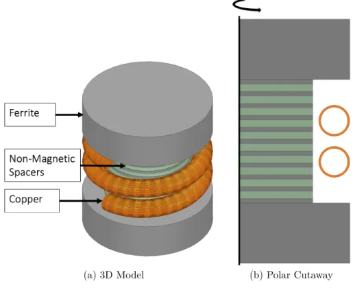
The proposed inductor structure uses a dumbbell-shaped core geometry with quasi-distributed gaps in the center post (Fig. 3-1). The center post is constructed of
alternating discs of ferrite and non-magnetic spacer material (e.g. plastic). Large ferrite end caps bookend a single-layer winding, which can be implemented with a
copper tube. The end caps shape the flux path so that a reduced portion of the flux fringes axially out of the core (i.e. out of the “top” and “bottom” in Fig. 3-1).
(a) 3D Model (b) Polar Cutaway
Figure 3-1: CAD model of the RF distributed gap inductor. Note that the polar cutaway of the structure doesn’t account for the spiral nature of the coil.
3.2.2
Field Balancing and Quasi-Distributed Gaps for
Im-proved Performance
In high-frequency inductors, current carrying is limited to conductor surfaces by skin
effect, and current crowds towards conductor surfaces near larger magnetic fields. Field balancing, a design approach centered around the distribution of the magnetic
fields around the conductors [14], [15], is one key technique used to dramatically in-crease the attainable performance in the proposed structure. Through this technique,
the copper loss is reduced by maximizing the effective conduction area available in the wire to carry current by providing balanced fields on the wire surfaces.
In the structures in [14], [15] and in the proposed structure (Fig. 3-1), the magnetic field flowing up the center post and flowing back down the return path can be balanced
to yield “double-sided conduction” in the wires, i.e. a skin of conduction close to the center post and a skin of conduction on the opposite side of the wires. In order to do
− +
𝑁 𝑖
ℛfringe
Figure 3-2: Magnetic circuit model for the “dumbbell” inductor. ℛcenterrepresents the magnetic path within the barrel of the solenoid while ℛfringe represents the magnetic path outside of the solenoid. The reluctance of the end caps is treated as negligible.
so, the reluctances in the magnetic circuit must be carefully designed. The magnetic
circuit model for the proposed solenoid “dumbbell” inductor is shown in Fig. 3-2, in which the end cap reluctances are approximated as being negligible. ℛcenter models
the lumped reluctance provided by the distributed gap core in the “barrel” of the solenoid while ℛfringe models the reluctance of the flux return path outside of the
solenoid. If these reluctances are equal, they sustain the same MMF drop and hence the same 𝐻 = 𝑑(𝑀 𝑀 𝐹 )𝑑𝑙 on both sides of the wire, yielding two layers of conduction.
An ANSYS finite element simulation [1] illustrates this effect in Fig. 3-3.
Figure 3-3: ANSYS FEA simulation illustrating the current crowding phenomenon. For the conductor on the right, the left hand side of the conductor is adjacent to the barrel of an air-core solenoid, a region with high reluctance and MMF drop com-pared to the outside of the solenoid. This MMF imbalance creates an asymmetry in the current distribution and increases loss. The conductor on the left is a miniatur-ized version of the wire in the proposed inductor and experiences much less current crowding due to the balanced nature of its surrounding magnetic fields. The example simulation runs at 13.56 MHz with an excitation current of 20 𝐴𝑝𝑘. The wires are 0.8
mm in diameter with the conductor on the right being part of a larger solenoid with an inner diameter of 6 mm.
The reluctance of the center post is set by using a quasi-distributed gap [7] as
opposed to a single large gap. The quasi-distributed gap can greatly reduce eddy current losses caused by magnetic fields fringing from the gap(s) [7]. By increasing
the number of gaps used in the structure, the strength of the fringing fields is reduced and the copper is able to be placed closer to the center of the structure. However,
thin discs suffer from a lack of mechanical rigidity and increased complexity, forcing a design tradeoff.
The reluctance of the return path is set by the overall size of the structure (ℛfringe ≈ 𝜇0𝜋𝑟0.9𝑡 2[13]). Here we see that the return-path reluctance decreases with the size of the structure, and therefore at a certain size and inductance target it is necessary to eliminate any other parallel return-path reluctance like the outer shell
of a pot core. That is, to achieve perfect double sided conduction, ℛfringe = 𝑁
2
2𝐿desired.
This requirement forces a strict relationship between the outer radius of the inductor
𝑟𝑡 and the number of turns 𝑁 where 𝑁 may be similarly constricted to small values
to reduce the copper loss incurred.
𝑟𝑡=
1.8𝐿desired
𝑁2𝜇 0𝜋
(3.1)
A python script (Appendix B) was developed which outputted design geometries to
achieve double-sided conduction. Given user input variables such as desired induc-tance, number of turns and gaps, the script returns the design geometries required
the simulate and construct the inductor.
3.2.3
Optimum Aspect Ratio
Given the lack of first principles models of the losses within the structure, several
manual sweeps are required to achieve an inductor which minimizes loss. One such design handle is the structure’s aspect ratio (defined as total diameter to height).
Smaller aspect ratios (i.e. taller, skinnier inductors) create a very long magnetic path
2Valid for structures where ℎ
𝑡 > 23𝑟𝑡 where 𝑟𝑡 and ℎ𝑡 are the outer radius and height of the
0.7 0.75 0.8 0.85 0.9 0.95 1 0
500 1,000 1,500
Aspect Ratio (diameter:height)
Q
Figure 3-4: Quality factor vs. Aspect Ratio. Several inductor designs were simulated with inductance, number of turns, and number of gaps constrained. Here it was found that the optimal aspect ratio was 0.9. Note, since the outer radius of the inductor is constrained per Equation 3.1, the volume of the inductor is variable. However, larger volumes do not necessarily imply larger quality factors. The design point of 𝑘 = 0.9 is also maximal on the Q vs. volume curve.
for flux to flow and provide very little core area. These two factors yield large core loss and create a lower bound on the aspect ratio. On the other end, large aspect
ratios (short, pancake-like inductors) constrain the usable wire diameter, yielding large copper losses. In between these two extremes, a low-loss design can be achieved.
An example of one such sweep is shown in 3-4. Here, the optimal aspect ratio was found to be 0.9.
3.2.4
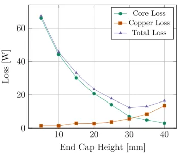
End Cap Height
Although the reluctance of the end caps may be approximated as negligible compared
to the reluctance of the distributed gaps, the loss within these elements may not be disregarded. Increasing the end cap height (thickness) helps to reduce the flux density
and thus core loss within the pieces. However, the copper wire diameter must be reduced to accommodate the smaller window area, increasing copper loss
Given the difficulty of creating a model that fully captures this tradeoff, a manual sweep was done. With volume and 𝑟𝑡constrained, the end cap height was varied. The
10 20 30 40 0
20 40 60
End Cap Height [mm]
Loss
[W]
Core Loss Copper Loss
Total Loss
Figure 3-5: End Cap Height Sweep. After constraining the outer radius, 𝑘, induc-tance, number of turns, and number of gaps, the height of the end caps was varied. This design sweep illustrates the the tradeoff between core loss within the end caps and copper loss in the windings. The optimal loss balance to minimize total loss is found when core loss and copper loss are approximately equivalent.
results of this sweep are shown in Fig. 3-5. The volume of the inductor is constrained
to be 1.16 × 10⁻³ m3 and the total radius is 57 mm. The total loss of the inductor is minimized at end cap height = 30 mm. This design point strikes the balance of core
loss in the end cap and copper loss in the windings.
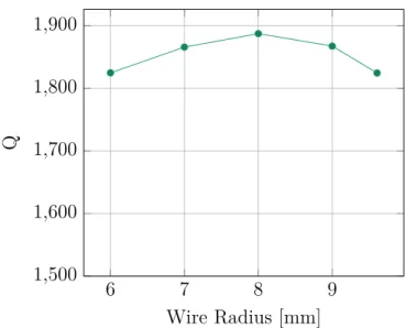
3.2.5
Wire Size and Capacitance
Finally, selecting the optimal wire size presents the final manual search space required to generate an optimized low-loss inductor. The wire size presents a trade off of
conduction loss and capacitance. It was found that the most dominant capacitance within the structure was the turn-to-turn capacitance of the copper coils. Thus by
reducing the wire diameter and increasing the spacing of coil, the winding capacitance will be reduced at the expense of increased conduction loss. An example of one such
sweep is shown in Fig. 3-6. The Q reported accounts for circulating currents created by the equivalent parallel capacitance of the structure. This estimated capacitance is
generated by ANSYS Maxwell. However, Maxwell was found to seriously under-report the actual capacitance. All other variables except wire diameter were constrained.
6 7 8 9 1,500 1,600 1,700 1,800 Wire Radius [mm] Q
Figure 3-6: Wire Radius Sweep. By reducing the wire radius, the turn-to-turn capac-itance is reduced, yielding smaller circulating currents due to this capaccapac-itance and increasing efficiency. However, this reduction in wire radius yields a smaller conduc-tion area and thus increases conducconduc-tion loss forcing a tradeoff. The quality factor presented here accounts for the turn-to-turn capacitance although this capacitance may be smaller than would be measured in real life as discussed in Section 5.5.
3.2.6
Loss Distribution
Generally in magnetics, designers are given the freedom to trade core and copper loss to minimize total loss through several design handles such as the number of turns.
Typically, the overall loss of the element is minimized when the two losses are roughly equivalent; specifically the optimum ratio of core loss to copper loss is 2
𝛽, where 𝛽 is
the Steinmetz parameter for the magnetic material [9]. In this design space, however, it is desirable to penalize large core losses more than large copper losses. First, due
to the high thermal conductivity of copper and the ability to remove heat through liquid cooling flowing through the center of the pipe, it is much easier to remove heat
from the windings than the core pieces. Second, ferrites are prone to fracture under high thermal stress, and the core losses grow with temperature, yielding the potential
for thermal runaway and designs that perform poorly under steady-state (rather than pulsed) operation.
3.3
Conclusion
This chapter presents a design approach for high-power inductors at RF frequen-cies (e.g., kW power scales at tens of MHz) that expands upon previously-developed
techniques for high-frequency inductors at more modest power levels. The proposed design approach leverages low-permeability high-performing RF magnetic materials,
single-layer windings, quasi-distributed gaps and field balancing to mitigate loss. The next chapter will provide detail about an example design.
Chapter 4
Example 580 nH Inductor Design
and Construction
An example 580 nH inductor design using the proposed dumbbell structure (Fig. 3-1, repeated here as Fig. 4-1) was developed, simulated, constructed and experimentally
tested. In simulation the design achieves a quality factor of ∼1700 at 13.56 MHz and 80 𝐴𝑝𝑘; as will be shown, the experimental quality factor has been difficult to
accurately determine to date, but is at least 1100, and some measurements done suggest that it is approximately 1600. The inductor, whose structure is shown in Fig.
3-1, is approximately 100 mm in diameter and 110 mm in height. It uses Fair-Rite 67 as the core material and polypropylene for the plastic spacers for the distributed
gap. Fair-Rite 67 was chosen as the core material as it was recently characterized [4], [6] to be high-performing in this frequency range and is a key enabler to the design’s
success. The winding is a custom wound 16 mm diameter copper tube with two full turns. A picture of the prototype inductor can be seen in Fig 5-3b.
4.1
Simulation Results
Presented in the following figures are simulation results from ANSYS Maxwell 2D
Eddy Current solution solver. Simulations were run at an operating frequency of 13.56 MHz and peak current excitation of 80 𝐴pk. Core loss data for Fair-rite 67
cutaway of the structure doesn’t account for the spiral nature of the coil.
Outer Radius 56.977 mm
End Cap Height 31.284 mm
Center-Post Radius 37.763 mm Center-Post Ferrite Thickness 2.275 mm
Total Height 126.613 mm
Number of Gaps 10
Wire Diameter 16 mm
Number of Turns 2
Magnetic Core Material Fair-rite 67 Plastic Spacer Material Polypropylene
Figure 4-2: Magnetic Flux Lines of Proposed Inductor. The field lines on either side of the winding are well balanced yielding current sharing between the inner and outer sections of the winding, reducing copper loss. The simulation assumes a system temperature of 25∘C with a fair-rite 67 core relative permeability of 𝜇
𝑟 = 40 and
copper bulk conductivity 𝜎𝑐𝑢= 58000000 Siemens/m and copper relative permeability
of 0.999991.
was gathered using the techniques described in Chapter 2 and input into the FEA
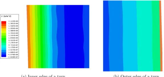
solver1. Fig. 4-2 demonstrates the balanced nature of the magnetic fields on either side of the winding while Fig. 4-3 shows the current distribution due to these fields.
At a system temperature of 25∘C and copper bulk conductivity of 𝜎𝑐𝑢 = 58000000
Siemens/m and copper relative permeability of 0.999991, the simulated copper loss is
43.434 W while the simulated core loss is 17.742 W yielding a total loss of 61.176 W. This coupled with the reported inductance of 500.56 nH yields a Q of 2120. If the
equivalent parallel capacitance is assumed to be 30 pF, the simulated quality factor at 80 𝐴pkis 1697. In general, this capacitance is hard to predict, however given previous
experimental results, this capacitance figure is reasonable for an inductor of this size
4.2
Inductor Construction
The copper windings are constructed of DHP C122 copper from coppertubingsales. com. The outer diameter of the winding is 16 mm and its wall thickness is 1 mm.
1Gathered 𝑃
𝑐𝑣 v. 𝐵 data was input into the solver.^ Maxwell then extracts the Steinmetz
edges of the turns carry significant current, reducing copper loss. The simulation assumes a temperature of 25∘C and a copper bulk conductivity of 𝜎𝑐𝑢 = 58000000
Siemens/m and copper relative permeability of 0.999991.
The pitch of the coil is approximately 32 mm. The copper winding was formed from
annealed copper tubing via a custom designed former fixture, shown in Fig. 4-4. After filling the annealed tubing with sand and sealing off either end, the tubing is
inserted onto the fixture which is then affixed to a chuck. By rotating the chuck and bending the tubing, the copper coil can be formed.
Appendix F illustrates the CAD drawings used to manufacture the ferrite discs. Fair-rite both provided the magnetic material and manufacturing necessary to build
the inductor. 1/8” thickness polypropylene plastic spacers were cut using a water jet in-house to form the distributed gap. The radius of these spacers was the same as the
center-post ferrite discs. A circular cut-out in the center 2 mm in diameter was used in conjunction with a 1/16” diameter carbon fiber rod to ensure the concentricity of
the discs.
In total, both end caps are made from two stacked 615.5 mil thick end cap pieces.
The distributed gap is formed by alternating layers of 11 pieces of 89.6 mil thick ferrite and 10 pieces of 1/8” thick polypropylene (with ferrite forming the ends of the
Figure 4-4: Copper Coil Former Fixture. The grey cylinder which the copper coil is wound around is a PVC rod 40 mm in diameter. Steel bolts are used to hold the right end of the coil in place as the cylinder is rotated and the coiled formed.
Chapter 5
Quality Factor Measurement Test
Fixture
This chapter introduces the necessity and difficulties associated with characterizing the loss of high Q inductors at high currents and frequencies. It also demonstrates
some useful techniques for overcoming these difficulties.
5.1
Motivation
An important aspect of developing high-quality-factor magnetic-core inductors is
be-ing able to accurately characterize their losses. Experimental validation of the quality factor at high power is challenging for many reasons. First, the losses in the ferrite
are nonlinear, requiring the measurement setup to operate at the rated current of the inductor (in this case, 80 𝐴𝑝𝑘). Second, the very low losses in the inductor (equivalent
series resistance on the order of tens of mΩ) are difficult to distinguish from other small losses in the test fixture. Finally, accurately measuring currents at RF is
dif-ficult; at minimum it requires expensive measurement hardware that may introduce additional loss in the system. Consequently it is best if the measurement technique
relies only on the measurement of RF voltages or low-frequency (e.g., DC) voltages and currents.
are designed for 50 Ω systems. This has two main implications: first, to produce the required drive current (80 𝐴𝑝𝑘), the power amplifier would have to have a power
rating of over 160 kW, a very large and expensive object. Second, although the power amplifier may be able to handle loads that are not exactly 50 Ω, the harmonic
content begins to stray very far from the single-tone requested of the amplifier, cre-ating measurement inaccuracies. These two issues necessitate a measurement system
that presents 50 Ω to the input port and turns 50 Ω voltages and currents into low impedance voltages and currents (to obtain the higher drive current required).
The resonant tank method for measuring quality factor explored in Chapter 2 has the promising benefit of requiring only RF voltage measurements to extract the
resistance of the inductor. A setup for this structure is illustrated in Fig. 5-2. To obtain the equivalent resistance 𝑅𝐿 (and thus quality factor) of the inductor, first the
capacitance or operating frequency must be tuned to resonance. Resonance can be found either when 𝑣inputand 𝑣reso are 90∘ out of phase or when the maximal gain (i.e.
𝑣reso
𝑣input is maximized) is achieved. Assuming 𝐶reso has internal resistance 𝑅𝑐 and that
there exists resistance external to the D.U.T., in series with the tank 𝑅𝑥:
𝑣reso = 𝑣input
(𝑗𝜔𝐶reso)−1+ 𝑅𝑐
𝑗𝜔𝐿 + 𝑅𝐿+ 𝑅𝑥+ 𝑅𝑐+ (𝑗𝜔𝐶reso)−1
(5.1)
At resonance: 𝑣reso = 𝑣input
(𝑗𝜔𝐶reso)−1+ 𝑅𝑐 𝑅𝐿+ 𝑅𝑥+ 𝑅𝑐 (5.2) 𝑅𝐿 = 𝑣input 𝑣reso ⃒ ⃒ ⃒ ⃒ ⃒ 1 𝑗𝜔𝐶reso + 𝑅𝑐 ⃒ ⃒ ⃒ ⃒ ⃒ − 𝑅𝑥− 𝑅𝑐 (5.3) 𝑄𝐿 = 𝜔𝐿 𝑅𝐿 (5.4)
𝑅𝑥 can be estimated using finite element software upon the linkages connecting the
D.U.T. to the capacitor and 𝑅𝑐was obtained using the vacuum capacitor’s datasheet.
𝑅𝑥 was estimated to be 4.8 mΩ and 𝑅𝑐 was reported to be 4.14 mΩ.
A challenge with the resonant tank approach is that the resistance presented by
the resonant tank at the operating point is far from 50 Ω, and requires higher current than a practical 50 Ω PA can provide, as described above. Consequently a substantial
degree of impedance transformation (or, equivalently, voltage and current
transfor-mation) is needed. However, by using a transformer to couple the PA (a 50 Ω system) to the resonant tank (a 10s of mΩ system), both requirements of input impedance
matching and measurement ease can be achieved. This design - incorporating an
𝑁 : 1 transformer - is shown schematically in Fig. 5-2.
5.2
Transformer-Based Test Fixture Design
The test fixture design shown in Fig. 5-2, adapted for high power operation from
the design in [4], allows us to measure the inductor quality factor at very high RF power levels and kV-scale RF voltages. This technique is extremely beneficial as
it allows the user to extract the inductor’s quality factor by measuring the ratio of two single-ended voltages’ amplitudes. The D.U.T. is resonated with a low-loss
vacuum capacitor and transformer-coupled to an RF power amplifier to drive pure-tone, high current sinusoids into the system. From measurements of the voltage
across the transformer (𝑣input) and the resonant capacitor (𝑣reso,div), one can calculate the resistance of the system and the inductor quality factor can be obtained. The
injection transformer was implemented with 20 turns of triple insulated litz wire (Rubadue wire, 230 strands/44 AWG litz, PN TXXL230/44F3XX-2(MW80))) on
a Fair-rite 67 toroid (PN 5967003801). The transformer’s primary-referred leakage inductance was estimated to be 8.5 𝜇H and magnetizing inductance 13.5 𝜇H1. The
copper tubing used to connect the inductor to the vacuum capacitor formed the single secondary turn.
Given the high quality resonance and large drive levels, a very large voltage is developed across the vacuum capacitor (≈ 4.7kV at the full drive current of 80 𝐴pk).
In order to measure this RF voltage, a capacitor divider was used, shown schematically in Fig. 5-1. This voltage divider circuit is shown as the green PCB on the left in the
Fig. 5-3a. The PCB contains a stack of 10, 5 pF Mica capacitors in series with a 22
1The transformer’s leakage inductance was estimated using the leakage tuning capacitance 𝐶 leak
described in Section 5.2.1. The transformer’s magnetizing inductance was estimated using the man-ufacturer’s 𝐴𝐿 value with 𝑁 = 20 with the leakage inductance subtracted from this value.
RF IN 22 pF
Figure 5-1: Capacitor Voltage Divider Schematic. The voltage across the 22 pF ca-pacitor is 2.22 % times the “RF IN” input voltage. The caca-pacitors used were all of type MC 1210 from Cornell Dubilier Electronics. Note, in reality there are parasitic capacitances that couple to the divided down node across the 22 pF capacitor, im-pacting the voltage division ratio.
pF Mica capacitor (Cornell Dubilier Electronics Type MC, 1210 size). Yielding an unloaded voltage division ratio of 2.22%. The schematic and layout for this PCB are
provided in Appendix D. However, this division ratio is impacted by other external capacitances such as capacitance due to proximity to the conductive vacuum capacitor
body or load capacitance in parallel with the 22 pF capacitor. The board is made of Rogers 4350B, low-loss PCB substrate and copper foil is used to connect the pads
of the PCB with a screw on the capacitor plate. The vacuum capacitor (𝐶reso in Fig. 5-2) used was a Comet-PCT 50-500 pF variable vacuum capacitor with peak RF
voltage capability of 9 kV (PN CVPO-500BC/15-BECA).
Fig. 5-3 illustrates both the CAD model of the test fixture shown schematically
in Fig. 5-2 and the physical system. All copper elements were silver-plated with 0.5 mil of silver (plated by F. M. Callahan &: Son Inc. company of Malden, MA). The
silver plating helps reduce the degradation of the copper surfaces over time as copper oxide is a semiconductor at room temperature while silver oxide is still considered
a conductor. CAD drawings for the capacitor plates (1/4” thick 101 copper from McMaster-Carr) and other mechanical fixturing details are provided in Appendix G.
The connecting tubing is formed from 16 mm outer diameter, 1 mm wall thickness DHP C122 copper from coppertubingsales.com. Solder-connect elbow and reducer fittings from McMaster-Carr were used to connect the capacitor plates to the inductor.
Signal Generator PA 𝐶leak N:1 D.U.T. 𝐶reso + − 𝑣reso + − 𝑣input + − 𝑣reso,div
Figure 5-2: Simplified Inductor Quality Factor Measurement Fixture Schematic. The D.U.T. inductor is resonated with a low-loss capacitor. The series resonant tank is transformer coupled to a power amplifier in order to present an impedance close to 50 Ω to the PA and extract a pure tone. The large resonant node voltage is divided down and measured using a capacitor divider shown in the right of this figure. 𝐶leak resonates out the transformer’s leakage inductance as discussed in 5.2.1. Note the transformer schematically shown here is not ideal and includes parasitics such as leakage and magnetizing inductance and winding and core resistances.
(a) CAD Model (b) Setup
Due to the nature of operating at RF, there are many parasitics in the system that either need to be calibrated out or otherwise avoided. Given the nature of the
single-frequency, sinusoidal operation of the system, resonance is a very powerful tool able to turn pesky parasitics into shorts or opens. One such parasitic is the leakage
induc-tance of the transformer. It causes a decrease in the series resonant frequency of the tank when viewed at the power amplifier port of the transformer rather than looking
directly into the resonant tank of interest. This is undesirable as the impedance of the tank (looking into the PA’s transformer port) at the maximal gain frequency may
have a significant inductive component, degrading the input match and the quality of sinusoids produced by the power amplifier. However, this nonideality can be resolved
by the insertion of a capacitor in series with the transformer leads (𝐶leak in Fig. 5-2).
By tuning this capacitor to resonate with the transformer’s leakage inductance at the frequency of interest (the maximal gain frequency of the resonant tank), the leakage
inductance’s adverse impact can be negated. An impedance analyzer (Agilent 4395A) was used to extract the impedance vs. frequency looking into the transformer port
seen by the PA and the capacitance was tuned such that the frequency of minimum reflection (i.e. minimum |ΓL|) coincided with the maximal gain frequency of the tank. The capacitors used were ATC 100B placed on a PCB made of Rogers 4350B sub-strate2. Finally, the reactive voltage these capacitors sustain may be larger than the
voltage rating of a single, reasonably sized capacitor, requiring the use of a series stack of capacitors.
Lastly, the turns ratio of the transformer must be tuned to obtain a series resonant impedance as close to 50 Ω as possible. However, the turns ratio isn’t as simple
as 50 Ω = 𝑁2(resonant tank impedance). This turns ratio must be determined experimentally. In general, the minimum of the input impedance |𝑍in| is not the series resonant impedance, illustrated in Fig. 5-4. Because of this, the number of
2The PCB used to mount these capacitors was the same as the capacitor divider PCB (Appendix
D), with material manually removed such that only the top 7 capacitor pads and input pad was present.
1.3 1.32 1.34 1.36 1.38 1.4 ·107 31.6 100 316 Frequency [Hz] |𝑍 in |[ Ω] 1.3 1.32 1.34 1.36 1.38 1.4 ·107 0 0.2 0.4 0.6 0.8 1 |Γ𝐿 | |𝑍in| |Γ𝐿|
Figure 5-4: Example Input Impedance. Note that the frequency where |𝑍in| is minimal is not the same as the frequency where |Γ𝐿| is minimal, where resonance actually
occurs. Data gathered using an Agilent 4395A.
turns should be tuned such that the impedance at the frequency where |Γ𝐿| is minimal,
not the frequency where |𝑍in| is minimal, is as close to 50 Ω as possible. This effect is due to the long transmission line that connects the PA/impedance analyzer to the tank and primary capacitance on the transformer. In general, the order of operations
for parasitic tuning is first choosing the correct number of primary turns to yield the correct resonant impedance then adjusting the leakage capacitance such that the
minimum reflection frequency and maximal gain frequency of the tank are coincident.
A full schematic illustrating these parasitics is provided in Fig. 5-5. A photo
illustrating the PCB which contained 𝐶leak is provided in Fig. 5-6.
5.2.2
Transformer Power Handling
To process the full load current required, the injection transformer is placed under considerable stress. Its large turns ratio and the 100s of watts that flow through this
device can yield considerable core and copper loss. Thus, design of the transformer must be executed with this limitation in mind. This is especially problematic if
the system is operated off resonance as the large reactive voltages generated by the resonant tank appear across the magnetizing inductance of the transformer, inducing
Signal Generator 𝐶pri 𝐿𝜇 𝑅𝐶 𝐶reso 𝑅𝑥 + − 𝑣input + − 𝑣reso,div + − 𝑣reso
Figure 5-5: Inductor Quality Factor Measurement Fixture Schematic Including Par-asitics. 𝐶pri models the equivalent primary capacitance of the transformer. Values for the transformer parasitics are given in section 5.2 while values for the parasitic resistances of the secondary tank are given in section 5.1. Resistors which model the transformer’s winding and core loss are not included.
Figure 5-6: Birds’ Eye View of Transformer Coupled Resonant Tank Test Fixture. The green PCB in the bottom left of the photo houses 𝐶leak. By manually tuning this capacitance, the impact of the transformer’s primary-referred leakage inductance can be nulled.
considerable core loss.
5.3
Local Rectification/RF Detection
5.3.1
Earth Abnormalities
For safety reasons, lab equipment, such as amplifiers and oscilloscopes, reference
their grounds to the mains’ earth connection. This is incredibly important as if there is a failure such that the chassis of the case or ground terminal is live with mains
voltage, a breaker can trip and users are protected. This safety feature however creates complications in that the earth connection provides a path for common mode currents
to flow. Both the power amplifier and oscilloscopes used in this setup connected the negative terminal of the output and probe input, respectively, to earth (illustrated
in Fig. 5-8). These two connections to earth were shorted together through the lab bench.
At low frequencies of operation, these two systems are isolated by action of the
transformer. However, due to parasitic capacitive coupling between the transformer windings, at high frequencies this isolation barrier breaks down and currents are able
to capacitively couple across the transformer. This isolation-jump coupled with the earth connection present on the oscilloscope provides a potential path for currents to
flow from the PA’s (earthed) negative terminal, capacitively couple to the secondary and flow through the scope’s earth connection back to the PA. Additionally,
conven-tional differential probes are not an adequate solution. Low voltage differential probes that may have enough capacitive isolation from differential input to ground often
can-not withstand the voltage required and high voltage differential probes typically have too much capacitance from differential input to ground to isolate the oscilloscope’s
earth from the measurement system. Potentially, optically isolated differential probes possess both the isolation and voltage headroom required. However, at the time of
writing, the cost of this solution was prohibitive.
causing measurement inaccuracies. The most significant being the use of a “ground
to ground” probe where a 3rd probe was connected to the tank with both the ground and signal lead connected to the same point on the bottom capacitor plate, shown in
Fig. 5-7. Normally this configuration is viewed as a sort of magnetic field detector as the voltage across the loop is proportional with the time derivative of flux passing
through the loop formed by the probe ground lead. However, this configuration is also able to detect differences in ground potentials which could be created by common
mode currents flowing into the scope and into the mains earth connection. When connected to the tank and scope, this “ground to ground” probe measured a voltage
of 3.5 Vpp. This voltage was significantly higher than any voltage measured near the inductor where the magnetic field strength would be highest, indicating that the
voltage is primarily due to ground currents rather than magnetic fields. Additionally, the probe caused a peculiar reduction in output voltage when plugged into the scope.
If the probe was unplugged from the scope (but still connected to the tank), the output voltage was 17.05 Vpp however on plugging the probe into the scope, the
output voltage was reduced to 3.5 Vpp. This is likely due a combination of a shift in tank resonant frequency and ground currents.
Signal Generator PA Mains Earth Probe Ground Probe Ground Mains Earth
Figure 5-8: Schematic illustrating earth connections
RF IN
𝐶1 𝐷2
𝐷1 𝐶2 𝑅
DC OUT
Figure 5-9: Voltage Doubler RF Probe Schematic. The parts list for the PCB which implements this schematic is given in Table 5.1. Appendix E includes the schematic and layout design files.
5.3.2
Voltage Doubler RF Probe
In order to circumvent the issues introduced by passing an earthed RF connection from the scope to the resonant tank, an RF detection approach based on local
rectifi-cation of the sensed AC voltage was used [2]. Per Equation 2.3, only the amplitudes of the RF waveforms are required to calculate the quality factor of the inductor as
long as the harmonic content is low and Q is calculated at the maximal gain point of the tank.
By rectifying the RF voltage, producing a DC voltage proportional to the peak of the RF voltage applied to the rectifier, a DC signal proportional to the RF voltage can
be synthesized, and read by an isolated multimeter, eliminating the issue introduced by the earth connection in the oscilloscope. Essentially, this technique uses diodes to
convert the signal of interest from the RF frequency down to DC where it can be read without interference, and where any broader EMI generated by the setup becomes
unimportant. To implement the probe detector, the voltage doubler rectifier topology was used (shown schematically in Fig. 5-9). This topology presents a high impedance
100 200 300 400 0 2 4 𝑉in[𝑉𝑝𝑝] 𝑉out [𝑉𝐷 𝐶 ]
Raw Calibration Data Linear Trendline, 𝑅2= 1
Figure 5-10: Example Voltage Doubler RF Probe and Capacitor Divider Calibration. A large RF voltage is applied to a 50 Ω resistor. The vacuum capacitor (used in the resonant tank) and capacitor divider are placed in parallel with this resistor. Graphed is the output voltage of the voltage doubler vs. the RF voltage applied across the 50 Ω resistor.
to the tank at DC, reducing the parasitic load presented by the doubler, and does not draw any dc current from the capacitor divider as some single-diode detectors might
do.
Calibration of the voltage doubler RF probe is especially important as the non-linear capacitances of the diodes (mainly functions of the DC voltage on the output
of the doubler) and the positioning of the doubler, which introduce variable parasitic capacitances, vary the transformation ratio of the capacitor divider on the resonant
node of the tank. An example of a calibration dataset (calibrating both the capacitor divider and voltage doubler) is shown in Fig. 5-10. An image of the data collection
setup is shown in Fig. 5-11 and is schematically shown in Fig. 5-12. Low capacitance Schottky diodes were used due to their short recovery times and reduced impact on
the transfer function of the capacitor divider. A full description of the RF probe design, including layout, connectors, etc., can be found in Appendix E.
Figure 5-11: Voltage Doubler RF Probe Calibration Fixture. an N connector Tee joins the RF input, the 50 Ω resistor, and a BNC Tee. A Lecroy PPE 4 kV probe connected to the oscilloscope and a BNC to test lead clip are connected to this BNC Tee. The test lead clips are attached to the vacuum capacitor to which the capacitor divider is connected. Finally, the RF probe is connected to the output of this capacitor divider.
Signal Generator PA 50 Ω 𝐶reso 0.5 pF 22 pF 𝐶1 𝐷2 𝐷1 𝐶2 𝑅 𝑉in 𝑉out
Figure 5-12: Voltage Doubler RF Probe Calibration Fixture Schematic
𝐶1 ATC 100B Series 120 pF
𝐶2 ATC 100B Series 1 nF
𝐷1 & 𝐷2 Macom MA4E1340B1 70 V Schottky diodes
𝑅 0805 2 MΩ||Multimeter Input Resistance (10 MΩ)
To validate the measurement methods presented above, an air-core inductor of similar inductance as the proposed inductor was constructed. Given the lack of non-linear
loss characteristics, the inductor’s quality factor can be measured at small signal with an impedance analyzer and compared with large signal measurements made using the
transformer-coupled resonant tank. The solenoid was constructed of 3 turns of 16 mm copper (wall thickness of 1 mm). The inner radius of the solenoid was 40 mm and
its pitch was 32 mm. Its inductance was measured as 532.03 nH at 13.56 MHz. This
inductor was also used as a basis for comparison with the cored prototype inductor.
Given the inductance and resistance of the solenoid, it is almost impossible for an impedance analyzer to separate the mΩs of inductor parasitic resistance from the
10s of Ω reactance when looking into the inductor directly. To solve this issue, the inductor is resonated with a vacuum capacitor at the frequency of interest. The
resonance nulls the reactive component of the series RLC circuit and the impedance analyzer is able to extract the resistance. Using this method, the small signal quality
factor obtained was 1096.3 The minimum impedance of this series resonant tank was
found to be 43.97 mΩ. After subtracting out DC resistance measurements of the connecting leads (estimated as 1.52 mΩ) and the capacitor ESR (approximately 4.02
mΩ), the inductor resistance was found to be 38.43 mΩ.
The large signal quality factor obtained by measuring a coreless inductor with the proposed resonant measurement setup was a Q of 1192 at 13.435 MHz and 𝐼pk= 19.47
A, corresponding to an estimated ESR of 37.7 mΩ. This result is very close to that
found via the small-signal measurement (considering the fixturing differences between the impedance analyzer measurement and the high-power test stand), validating the
measurement apparatus.
3The inductor used in this small signal Q measurement is slightly different from the large
sig-nal inductor and has an inductance of 508 nH. These differences are attributed to manufacturing differences between the two coils.
5.4.1
Inductor Effective Volume
To create a fair comparison between this air-core inductor and the proposed inductor, the “effective volume” of both structures were used. This volume was defined by the
minimum cylindrical volume surrounding the inductor such that the quality factor and inductance when placed within this metal box degraded by no less than 5%. This
box volume is indicative of the region of high-strength magnetic fields. The inner radius of the metal box was 257.77 mm with an inner height of 186.613 mm, yielding
a total volume of 38.95×10⁻³ m3. This constraint yielded the solenoid dimensions given above.
5.4.2
Q Spoiling
In order to provide a check on the validity of measurements made using the
trans-former coupled resonant tank and voltage doubler, an intentional, lossy element was added to the circuit. By inserting a 0.5” diameter steel rod into the “barrel” of the
air-core solenoid, the quality factor measured with the experimental system dropped from 1192 to 375, validating that the measurement apparatus is able to detect the
introduction of new losses into the system.
5.5
Results
The inductor quality factor was characterized using two methods. First one where
the RF waveforms 𝑣input and 𝑣reso,div were measured directly by an oscilloscope and the second using the voltage doubler RF probe method described previously.
The simulated and measured quality factor of the inductor are plotted in Fig. 5-13 as a function of peak current at 13.56 MHz. These measurements were obtained using
two single-ended probes and an oscilloscope. At the highest current point of 82.5 𝐴𝑝𝑘,
a Q of 1650 was achieved, nearly a factor of 3 better than a similarly-sized air-core
inductor at similar operating conditions (709 nH, 77.5 𝐴𝑝𝑘, 10.9 MHz, 𝑄 = ∼600)
0 20 40 60 80 100 0 500 1,000 1,500 Current 𝐴𝑝𝑘 𝑄
Proposed Inductor-Measured Proposed Inductor-Simulated 𝑄 = 600 air-core reference
Figure 5-13: Measured and Simulated Inductor Performance at 13.56 MHz as mea-sured with direct single-ended voltage measurements from an oscilloscope. It is noted that these experimental measurements were not repeatable at a later date, and that they are thus suspect.
However, these results were unable to be reliably replicated likely due to the common
mode noise and grounding issues covered previously and thus these measurements are suspect.
High current measurements using the voltage doubler technique were unable to be
obtained due to conducted EMI causing display instabilities on the Fluke multimeters used to measure the DC voltage. Future work involves eliminating the conducted
EMI issue, allowing the voltage doubler to run at the full power. Additionally, the capacitor divider ratio must be changed to reduce the peak output of the voltage
doubler (preventing failure of the Schottky diodes). The voltage doubler measurement method obtained a peak quality factor of 1134 at a current of 10.3 𝐴pk and 13.054
MHz.
5.6
Sources of Discrepancy
One source of discrepancy between the quality factor of a simulated inductor and one measured in the lab is the parasitic capacitance present across the coil leads.
(a) Thermal Image of Inductor (b) Thermal Image of Transformer
Figure 5-14: Thermal images of Inductor running at nearly full load current. The inductor is carrying 71.2 𝐴pk at 13.404 MHz. These images were captured with a FLIR E6 hand-held thermal camera.
𝐼series ESR 𝐿
𝐶par
Figure 5-15: Inductor Model Including Parasitic Parallel Capacitance
This capacitance resonates with the main inductor, causing additional currents to
flow through the inductor’s resistance, inducing additional loss. Illustrated in Fig. 5-15, given a fixed series current 𝐼series, additional currents will flow in the LCR
loop. Although the loss due to 𝐶par is easily calculated4, the actual capacitance is not. Thus coil simulation tools (such as Coil32) or finite element tools often severely
under-predict the quality factor of the inductors they simulate. For reference, Coil 32 estimates the quality factor of the comparison air-coil at 2540, however the peak
quality factor obtained was only 1096.
Additionally, several loss mechanisms within the test fixture were not modeled. Fringing fields that exit radially out of the end caps have the potential to impinge on
the connecting leads of the test fixture, inducing loss. Interconnect resistances of the solder-connect fittings, contact resistances between the capacitor plates and vacuum
capacitor, and the helical nature of the coil were also not modeled.
4The new Q which accounts for these circulating currents assumes a series R-L circuit where 𝐿 is
the same as inductance as a model which neglects 𝐶par and 𝑅new is the resistance required to yield
the same loss as RLC case. That is, 𝐼series2
technique is able to measure accurately is not known. As previously shown, quality factors up to 1100 are able to be detected by the doubler however, it is unclear that
if an inductor with a quality factor of 1800 is inserted in the system that the voltage doubler will report it as so.