HAL Id: hal-01736048
https://hal.archives-ouvertes.fr/hal-01736048
Submitted on 23 Mar 2018
HAL is a multi-disciplinary open access
archive for the deposit and dissemination of
sci-entific research documents, whether they are
pub-lished or not. The documents may come from
teaching and research institutions in France or
abroad, or from public or private research centers.
L’archive ouverte pluridisciplinaire HAL, est
destinée au dépôt et à la diffusion de documents
scientifiques de niveau recherche, publiés ou non,
émanant des établissements d’enseignement et de
recherche français ou étrangers, des laboratoires
publics ou privés.
On the microstructure of Si coimplanted with H+ and
He + ions at moderate energies
Shay Reboh, F. Schaurich, A. Declemy, J-F. Barbot, M.F. Beaufort, Nikolay
Cherkashin, P.F.P. Fichtner
To cite this version:
Shay Reboh, F. Schaurich, A. Declemy, J-F. Barbot, M.F. Beaufort, et al.. On the microstructure of
Si coimplanted with H+ and He + ions at moderate energies. Journal of Applied Physics, American
Institute of Physics, 2010, 108 (2), pp.023502. �10.1063/1.3459884�. �hal-01736048�
On the microstructure of Si coimplanted with
and
ions at moderate energies
S. Reboh, F. Schaurich, A. Declemy, J. F. Barbot, M. F. Beaufort, N. Cherkashin, and P. F. P. FichtnerCitation: Journal of Applied Physics 108, 023502 (2010); doi: 10.1063/1.3459884 View online: https://doi.org/10.1063/1.3459884
View Table of Contents: http://aip.scitation.org/toc/jap/108/2 Published by the American Institute of Physics
Articles you may be interested in
X-ray scattering study of hydrogen implantation in silicon
Journal of Applied Physics 99, 103509 (2006); 10.1063/1.2198928 Kinetic aspects of the growth of hydrogen induced platelets in SiC Journal of Applied Physics 87, 8415 (2000); 10.1063/1.373556
A lower bound on implant density to induce wafer splitting in forming compliant substrate structures Applied Physics Letters 70, 3519 (1997); 10.1063/1.119219
Hydrogen-implant induced exfoliation of silicon and other crystals Applied Physics Letters 71, 3519 (1997); 10.1063/1.120378
Mechanism of silicon exfoliation induced by hydrogen/helium co-implantation Applied Physics Letters 73, 3721 (1998); 10.1063/1.122875
Evolution of hydrogen and helium co-implanted single-crystal silicon during annealing Journal of Applied Physics 90, 3780 (2001); 10.1063/1.1389478
On the microstructure of Si coimplanted with H
+and He
+ions at moderate
energies
S. Reboh,1,2,a兲F. Schaurich,3A. Declemy,4J. F. Barbot,4M. F. Beaufort,4N. Cherkashin,2 and P. F. P. Fichtner3
1
PGCIMAT, Universidade Federal do Rio Grande do Sul, 91501-970 Porto Alegre, Brazil
2Groupe nMat, CEMES-CNRS, 29 rue J. Marvig, 31055 Toulouse, France
3Escola de Engenharia, Universidade Federal do Rio Grande do Sul, 91501-970 Porto Alegre, Brazil 4PHYMAT-CNRS, Université de Poitiers, 86962 Futuroscope, France
共Received 1 May 2010; accepted 3 June 2010; published online 19 July 2010兲
We report on the microstructure of silicon coimplanted with hydrogen and helium ions at moderate energies. X-ray diffraction investigations in as-implanted samples show the direct correlation between the lattice strain and implanted ion depth profiles. The measured strain is examined in the framework of solid mechanics and its physical origin is discussed. The microstructure evolution of
the samples subjected to intermediate temperature annealing 共350 °C兲 is elucidated through
transmission electron microscopy. Gas-filled cavities in the form of nanocracks and spherical bubbles appear at different relative concentration, size, and depth location, depending on the total fluence. These different microstructure evolutions are connected with the surface exfoliation behavior of samples annealed at high temperature共700 °C兲, determining the optimal conditions for thick layer transfer. 1.5 m thick Si films are then obtained onto glass substrates. © 2010 American
Institute of Physics.关doi:10.1063/1.3459884兴
I. INTRODUCTION
The fracture engineering of semiconducting materials implanted with hydrogen ions allows the transfer of single crystalline thin films onto host substrates.1,2It basically con-sists in the implantation of H+into a target substrate,
produc-ing a localized concentration that exceeds its solid solubility limit. The ballistic character of the implantation process also creates a high density of point defects and the undergoing microstructure modification generates a considerable lattice strain.3–5Hence, H-implanted substrates are thermodynami-cally unstable and the supply of thermal energy leads to the coprecipitation of H and vacancies in the form of nanosized crack-like cavities, mainly lying parallel to the surface.4 The preferential nanocrack orientation plays a crucial role in the layer transfer process and is related to an interplay between cavity nucleation and lattice strain.4,6 Nanocrack
evolves thermally via Ostwald ripening7 and subcritical
crack propagation8 and the complete overlayer separation is achieved when cracks coalescence sweeps the whole substrate.1,2
This process was originally conceived using H,1
how-ever, the total amount of ions to activate the process is con-siderably reduced by coimplanting H and He.9,10This effect has been attributed to a synergy between the H-chemistry, that stabilizes the internal surface of the crack and breaks the Si–Si bond at the crack-tip, and the efficient crack pressur-ization provided by He.8–10Although the main physic con-cept of the coimplantation has been realized, it is a complex system for which the microstructure evolution strongly
de-pends on experimental parameters, as the implantation order, energy range, and relative depth positions of H and He depth profiles.11
More recently, the investigation of moderate implanta-tion energy of H+and He+in Si, leading to micrometer-scale
depth penetration of the ions, provided significant informa-tion on fracture mechanism culminating in the layer separa-tion, demonstrating also the possibility to obtain freestanding films.12Furthermore, the development of a method to obtain and integrate single crystalline semiconducting films of micrometer-thicknesses is of great interest for thin-film solar cells fabrication. In this context, a series of recent break-throughs conducting to record energy conversion were achieved using multilayered structures.13,14However, the in-tegration of materials with significant lattice mismatch has been the main challenge in this field and is still limiting further improvements.
Here, we study the effects of H++ He+coimplantation in
the microstructure of共001兲 Si substrates, in connection with the development of micrometer-thick layer transfer. We start by investigating the strain in as-implanted samples, showing that the strain intensity enhances and the deformed region enlarges with increasing fluence. The depth-distribution of strain is found to be related to the implanted ions depth pro-file. An evolving contribution of H and He occurs for differ-ent fluences and the physical origin of strain is discussed. The microstructure developments after intermediate
tempera-ture annealing 共350 °C兲 are examined and correlated with
the strain distribution in the as-implanted state and with the surface exfoliation behavior upon high temperature anneal-ing共700 °C兲. The optimal fluence conditions for thick layer transfer via H + He coimplantation are found, and a Si layer of 1.5 m thickness is obtained onto a glass substrate.
a兲Electronic mail: shay.reboh@cemes.fr.
JOURNAL OF APPLIED PHYSICS 108, 023502共2010兲
II. EXPERIMENTAL
Czochralsky grown p-type共001兲 Si substrates with a re-sistivity of 1 – 25 ⍀ cm, were implanted with H+ions at 168 keV, followed by He+ions at 345 keV, respecting a 1H/1He ratio. The chosen energies provided coincident projected ion
range at ⬇1500 nm depth from the wafer surface.15 Three
samples were implanted at distinct total fluence ⌽T 共⌽H+
+⌽He+兲 of 2, 6, and 10⫻1016 cm−2, referred further as low
fluence 共LF兲, intermediate fluence 共IF兲, and high fluence
共HF兲, respectively. The implantations were carried out at room temperature, with the samples 7° off-axis and con-trolled current densitiesⱕ0.5 A cm−2. Thermal annealing of the samples was performed in high vacuum, either at 350 or 700 ° C during 1800 s, to, respectively, study the micro-structure evolution and surface exfoliation behavior of the samples.
As-implanted samples were characterized by x-ray dif-fraction 共XRD兲. 共/2兲 scans in the vicinity of the 共004兲 reflection of Si allowed to determine the lattice strain gradi-ent in the direction normal to the sample surface.5,12 The experiments were performed in an automated two circles
go-niometer, using a Cu K␣1 radiation provided by a 5 kW
RIGAKU RU-200 source with a vertical linear focus in com-bination with a quartz monochromator. The XRD curves
were simulated combining ion implantation15 and XRD16
codes.
Microstructure investigation after 350 ° C annealing was
carried out by transmission electron microscopy共TEM兲 in a
JEOL 2010 microscope, operating at 200 kV. The surface characterization of the samples upon 700 ° C annealing was
conducted by scanning electron microscopy 共SEM兲 in a
JEOL JSM-5800.
Samples implanted according to the parameters leading to optimized exfoliation were bonded onto glass substrates
by hydrophobic surface activation17 and annealed up to
600 ° C to obtain layer separation. The transferred films were characterized by TEM.
III. RESULTS
A. As-implanted samples
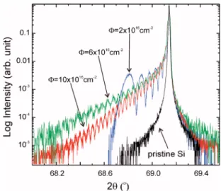
Figure 1 displays the XRD curves obtained from the
three implanted samples and a reference curve from a pris-tine substrate. All curves exhibit a main diffraction peak at 2B⬇69.14° rising from the undamaged crystal. For the
im-planted samples, the scattered intensity producing interfer-ence fringe patterns for ⬍2B is characteristic of a tensile
strain gradient of Gaussian-like shape.5The maximum strain 共max兲, given by the position of the last fringe away from the
Bragg peak, increases with the fluence. For the LF sample,
max⬇0.5%. For IF and HF samples, max could not be
de-termined due to the decreasing intensity diffracted by the highly strained region, which falls below the detection limit of the experiment. The drop of the intensity is related to the rising concentration of lattice damage.18However, the reduc-tion in the fringes spacing with increasing fluence points out the widening of the strain profile.5
B. Intermediate temperature annealing„350 °C and 1800 s…
Figure2 presents low magnification cross-section TEM
micrographs of the samples annealed at 350 ° C. The accu-mulated lattice damage appears as diffuse darker regions 共un-der bright-field diffraction contrast兲. The superimposed curves correspond to the ion and damage depth profiles esti-mated by the SRIM 共Ref.15兲 code. These curves are clearly
centered on the damage features observed by TEM. With increasing fluence, the damage distribution widens toward
the surface, enlarging from⬇85 nm at LF up to ⬇330 nm
for IF and⬇360 nm for HF. Figure 3 presents higher
mag-nification images of the damaged layers. For LF关Fig.3共a兲兴, nanocrack structures, observed in edge-on perspective, present diameters ranging from 30 to 80 nm and form within a narrow depth-distribution⬇80 nm wide. For IF 关Fig.3共b兲兴, the nanocrack diameter is smaller, sizing from 15 to 45 nm
and the depth-distribution widens to⬇120 nm. The majority
of the damaged region is formed by small spherical bubbles,
FIG. 1.共Color online兲 共/2兲 XRD scans close to the 共004兲 reflection of Si obtained from the samples implanted to⌽T= 2, 6, and 10⫻1016 cm−2and a reference curve from a pristine sample.
FIG. 2.共Color online兲 Low magnification cross sectional TEM micrographs of the samples implanted to⌽=2, 6, and 10⫻1016 cm−2and annealed at 350 ° C for 1800 s. The superimposed curves are the calculated profiles of the implanted ions and lattice damage.
with diameters ranging from 1 to 4 nm. Bubbles are observed in a region extending from the nanocracks layer up to⬇210 nm toward the surface. For the HF sample 关Fig. 3共c兲兴, the width of the nanocracks region is similar to the IF sample but the region containing bubbles widens. No significant modi-fication of the typical cavity size is observed. Regardless of the fluence, the distribution of nanocracks is centered at ⬇1530 nm depth, close to the projected range of the im-planted ions.
C. High temperature annealing„700 °C and 1800 s…
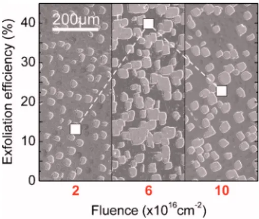
The exfoliation behavior of high temperature annealed samples was quantified in terms of an exfoliation efficiency parameter Aex, defined as the fraction of exfoliated area over
the specimen area. The obtained values are plotted in Fig.4, superimposed to SEM image of the corresponding sample. The trend of the curve characterizes an interval of fluences leading to optimal exfoliation. For the present experimental
conditions, the maximum Aex⬇40% occurs for 6
⫻1016 cm−2 共i.e., IF兲. Samples implanted to IF were then
hydrophobically bonded onto a glass substrate and annealed up to 600 ° C to obtain layer transfer. Figure5shows a cross-section TEM micrograph of the transferred film having an
estimated thickness of 1530⫾10 nm.
IV. DISCUSSIONS
Strain in ion implanted semiconductors originates from microscopic lattice defects that behave as point sources in-troducing isotropic intrinsic strainⴱ.19Along the directions parallel to the surface 共defined as x and y兲, the substrate stiffness causes an elastic reaction eyy= exx= −ⴱ, resulting in
unchanged lattice parameter. Thus, the relaxation of the lat-tice occurs along the z direction, i.e., toward the free surface, wherezz= 0. Therefore, the out-of-plane strain measured by FIG. 3. High magnification cross sectional TEM micrographs of samples
implanted to 共a兲 ⌽=2⫻1016 cm−2,共b兲 ⌽=6⫻1016 cm−2, and 共c兲 ⌽=10 ⫻1016 cm−2annealed at 350 ° C for 1800 s. The insets in the figure show a detailed image of a nanocrack 共a兲 and a spherical cavity 共b兲. The region between the dotted lines indicates the extension within the implanted layer that effectively contains nanocracks.
FIG. 4.共Color online兲 SEM micrographs of the samples annealed at 700 °C during 1800 s. The exfoliation efficiency values are plotted as a function of the total fluence superimposed to the respective sample image.
FIG. 5. Cross sectional TEM micrograph of a⬇1.5 m thick Si film trans-ferred onto a glass substrate.
XRD is the sum of intrinsic and elastic strains written as zz= ezz+ⴱ=共␦d/d兲z. The elastic component is introduced by
the compressive in-plane stressin-plane=yy=xxgiven by
in-plane= − 2
冉
␦dd
冊
Z, 共1兲
whereis the shear modulus of the substrate共⬇68 GPa for
Si兲.
The physical origin of the intrinsic strain is complex and depends on the implanted specie, its chemical-physical inter-action with the matrix and with the created lattice damage.20 Generally, in addition to the implanted atoms, the collision cascade produced by the incident ions mostly creates vacan-cies and self-interstitials in the matrix. Self-interstitial atoms introduce tensile strain in the lattice,21 and, in opposition,
vacancies generate compressive strain.20 For medium and
heavy ions implantation, such individual effects are clearer due to the reasonable spatial separation between vacancy, ion, and interstitial profiles.20–22 In the case of light ions as H+ and He+, the closer location of damage and ion profiles
renders a more intricate system. The approach adopted here to get an insight on the physical origin of strain is to first identify its characteristic depth-distribution. As the XRD measurements are not sensitive neither to the depth position nor to the symmetry of the profile,5 the reconstruction of strain distributions from the experimental curves is not straightforward, as it has multiple solutions. Thus, the ex-perimental curves were tentatively calculated assuming that the strain profile follows the simulated depth-concentrations of:共i兲 H atoms; 共ii兲 He atoms; 共iii兲 integrated H+He atoms; and共iv兲 self-interstitials. The more precise calculations were conducted for the LF sample for which the complete strain profile was accurately measured. Figure6presents the results along with the experimental curve. For this fluence, the simulations show that the shape of the measured strain
dis-tribution is intimately related to the H-disdis-tribution. Accord-ingly, the in-plane stress in the sample can be described re-placing the 共␦d/d兲zfactor in Eq.共1兲by a Gaussian function G共z兲 given by G共z兲 =
冉
␦d d冊
Z MAX e冉
− 共z − Rp兲2 2⌬R2p冊
. 共2兲 In Eq. 共2兲, 共␦d/d兲ZMAX is the maximum out-of-plane strainalong z and Rpand⌬Rpare the mean range and full width at
half maximum of the H-distribution. Figure 7 presents the
calculated stress of the LF sample. The maximum stress value is about 0.7 GPa.
Albeit the shape of the strain distribution for the LF sample is related to the H-distribution, the strain intensity is higher than what is expected for the implantation of 1016 H/cm−2 in Si.23 This demonstrates an effective contri-bution of He, which takes place within the previously im-planted H-profile. Upon annealing at 350 ° C, this sample only presented nanocracks confined in narrow layer共see Fig.
3兲, further indicating an effective interaction of He with the
H-rich region, as has been reported for low energy implants.24
For the IF and HF samples, the as-implanted strain sig-nificantly widens and the simulation of the XRD curves共not
shown兲 indicated a rising contribution of the He-related
depth-distribution as the fluence increase. This result can be discussed in connection with the depth-distribution of cavi-ties found upon 350 ° C annealing. The broadening of the cavity distribution was observed to be largely dominated by the formation of spherical bubbles above the nanocrack layer 共i.e., toward the surface, see Fig.3兲. This heterogeneous
mi-crostructure can be interpreted in terms of ion and vacancy depth-distributions. According to the simulated profiles
shown in Fig. 2, the H + He concentration is peaked at
⬇1540 nm depth, close to the observed nanocrack depth lo-cation at⬇1530 nm. The vacancy distribution is peaked at a
shallower depth of⬇1480 nm and largely extends toward the
surface, indicating that spherical bubbles form preferentially in the vacancy-rich region of the damaged layer. This obser-vation agrees with the concept that spherical bubbles result from the combination of gas atoms with a substantial amount
FIG. 6. 共Color online兲 Simulated and experimental XRD curves for the IF sample共⌽T= 2⫻1016 cm−2兲.
FIG. 7.共Color online兲 Calculated distribution of compressive in-plane stress in the LF sample共⌽=2⫻1016 cm−2兲.
of vacancies, whereas plate-shape cavities form preferen-tially under low vacancies availability.25,26A competitive be-havior for the consumption of gas atoms and vacancies can also explain the smaller nanocracks size concomitantly with the appearance of bubbles. Furthermore, as spherical-shape bubble formation is characteristic of He implantation in Si,27 it is speculated that in the present case it contains preferen-tially He atoms. Consequently, the significant widening of the strain profile is related to both the spreading of the im-planted region caused by the higher imim-planted fluence and to an increasing contribution of the expected He depth-distribution, which is initially wider than for H.
The general trend observed in the coimplanted samples is that the strain distribution is directly related to the im-planted ion profiles. This implies that significant interstitials and vacancies recombination render the damage contribution negligible out of the implanted ions profile. In the narrow region with high concentration of H and He, gas-vacancy
complexes and small cavities readily form during
implantation.27–30 The local consumption of vacancies also avoids interstitials annihilation which, in turn, can be stabi-lized by H up to high temperature.30Hydrogen also forms a
weakly bonded structure at the bond centered 共BC兲 and
an-tibonding共AB兲 site of the Si lattice.28However, this configu-ration stands only for as-implanted state vanishing at low temperature annealing. Differently, the contribution of He in the measured strain can only be attributed to gas-vacancy complexes.31 Thus, the physical origin of the strain in the as-implanted substrates cannot be assigned to a single type of defect but to a multiple contribution from pressurized gas-vacancy complexes, self-interstitials, and hydrogen atoms at the BC and AB positions of the lattice. Determining the par-ticular contribution of each type of defect remains challeng-ing and it certainly evolves upon annealchalleng-ing.
The exfoliation behavior of the samples submitted to high temperature annealing共Fig.4兲 showed the existence of
a range of fluences which enhances the surface exfoliation. The reduced exfoliation under LF conditions can be attrib-uted to the low amount of gas atoms involved in the process. Naturally, with increasing fluence the exfoliation is enhanced due to the higher content of gas atoms. However above a given fluence, unfavorable microstructure developments re-duce the exfoliation efficiency. In the present case, it was observed the formation/evolution of spherical bubbles com-peting with nanocracks. The absence of localized surface de-formation also implies that the strain induced by the cracks development is somehow relaxed by other mechanisms, such as localized plastic deformation. Plasticity effects in
nanocrack-tip have been predicted by calculations32 and
more recently, a mechanism of stress relaxation via plastic-regime interaction of nanocracks was observed.8Those phe-nomena may be favored in highly damaged substrates.
Finally, wafer bonding and Si layer transfer onto glass substrate was carried out using the implantation condition
leading to optimal exfoliation efficiency 共IF, ⌽T= 6
⫻1016 cm−2, see Fig. 4兲. The film thickness of ⬇1530 nm
共see Fig. 5兲 shows that the fracture process occurred along
the region of maximum nanocrack concentration. The ab-sence of treading dislocations in the transferred film for such
combination of materials with considerably distinct thermal expansion, show that the method can be further explored to obtain good quality micron-scale semiconducting materials integration.
V. CONCLUSION
In summary, the microstructure of H + He coimplanted Si was studied by XRD, TEM, and SEM. The strain distribution measured by XRD in as-implanted samples was found to be intimately related to the implanted ion depth profiles. For LF, the H-distribution shapes the strain profile and the contribu-tion of He occurs within the region previously implanted with H. For higher fluence this interaction is less effective and an increasing contribution of the He-profile was ob-served. The physical origin of strain was attributed to mul-tiple contributions from pressurized gas-vacancy complexes, stabilized self-interstitials and hydrogen atoms at the BC and AB positions of the lattice. Upon annealing at intermediate
temperature 共350 °C兲, TEM investigations revealed the
for-mation of crack-like and spherical cavities, being their oc-currence and depth-distribution strongly dependent on the fluence and ion/damage interaction. The surface exfoliation behavior of the samples was studied upon high temperature annealing共700 °C兲, showing that IFs lead to optimal condi-tions for layer transfer. LFs produce low exfoliation effi-ciency due to the low amount of gas atoms participating in the process. HFs generate unfavorable microstructure. Fi-nally, using the optimized implantation fluence, Si films ⬇1.5 m thick were transferred onto a glass substrate. The development of micron-scale thick layer transfer provides a method to integrate semiconducting films for high efficiency solar cells fabrication.
ACKNOWLEDGMENTS
The authors acknowledge the support of the Brazilian
agencies CAPES 共Process BEX 2358/09-3兲 and CNPq,
PETROBRAS S.A. and the Center for Electron Microscopy 共CME兲 of the Universidade Federal do Rio Grande do Sul 共UFRGS兲.
1M. Bruel,Mater. Res. Innovations3, 9共1999兲.
2B. Aspar, H. Moriceau, E. Jalaguier, C. Lagahe, A. Soubie, B. Biasse, A. M. Papon, A. Claverie, J. Grisolia, G. Benassayag, F. Letertre, O. Rayssac, T. Barge, C. Maleville, and B. Ghyselen, J. Electron. Mater. 30, 834 共2001兲.
3T. Höchbauer, A. Misra, M. Nastasi, and J. W. Mayer,J. Appl. Phys.92, 2335共2002兲.
4M. Nastasi, T. Höchbauer, J.-K. Lee, A. Misra, J. P. Hirth, M. Ridgway, and T. Lafford,Appl. Phys. Lett.86, 154102共2005兲.
5N. Sousbie, L. Capello, J. Eymery, F. Rieutorda, and C. Lagahe,J. Appl. Phys.99, 103509共2006兲.
6S. Reboh, M. F. Beaufort, J. F. Barbot, J. Grilhé, and P. F. P. Fichtner, Appl. Phys. Lett.93, 022106共2008兲.
7J. Grisolia, G. Ben Assayag, A. Claverie, B. Aspar, C. Lagahe, and L. Laanab,Appl. Phys. Lett.76, 852共2000兲.
8S. Reboh, J. F. Barbot, M. F. Beaufort, and P. F. P. Fichtner,Appl. Phys. Lett.96, 031907共2010兲.
9A. Agarwal, T. E. Haynes, V. C. Venezia, O. W. Holland, and D. J. Eagle-sham,Appl. Phys. Lett.72, 1086共1998兲.
10M. K. Weldon, M. Collot, Y. J. Chabal, V. C. Venezia, A. Agarwal, T. E. Haynes, D. J. Eaglesham, S. B. Christman, and E. E. Chaban,Appl. Phys. Lett.73, 3721共1998兲.
11P. Nguyen, K. K. Bourdelle, T. Maurice, N. Sousbie, A. Boussagol, X.
Hebras, L. Portigliatti, F. Letertre, A. Tauzin, and N. Rochat, J. Appl. Phys.101, 033506共2007兲.
12S. Reboh, A. A. de Mattos, J. F. Barbot, A. Declemy, M. F. Beaufort, R. M. Papaléo, C. P. Bergmann, and P. F. P. Fichtner,J. Appl. Phys.105, 093528共2009兲.
13J. F. Geisz, S. Kurtz, M. W. Wanlass, J. S. Ward, A. Duda, D. J. Friedman, J. M. Olson, W. E. McMahon, T. E. Moriarty, and J. T. Kiehl,Appl. Phys. Lett.91, 023502共2007兲.
14J. F. Geisz, D. J. Friedman, J. S. Ward, A. Duda, W. J. Olavarria, T. E. Moriarty, J. T. Kiehl, M. J. Romero, A. G. Norman, and K. M. Jones, Appl. Phys. Lett.93, 123505共2008兲.
15J. F. Ziegler, J. P. Biersack, and U. Littmark, The Stopping and Range of
Ions in Solids共Pergamon, New York, 1985兲.
16S. A. Stepanov,http://sergey.gmca.aps.anl.gov/
17Q. Y. Tong and U. Gösele, Semiconductor Wafer Bonding: Science and
Technology共Wiley, New York, 1999兲.
18P. H. Dederichs,J. Phys. F: Met. Phys.3, 471共1973兲.
19J. Qu and M. Cherkaoui, Fundamentals of Micromechanics of Solids 共Wiley, New York, 2006兲.
20J. P. de Souza, Y. Suprun-Belevich, H. Boudinov, and C. A. Cima,J. Appl. Phys.87, 8385共2000兲.
21S. Koffel, N. Cherkashin, F. Houdellier, M. J. Hytch, G. Benassayag, P. Scheiblin, and A. Claverie,J. Appl. Phys.105, 126110共2009兲.
22Y. Zhong, C. Bailat, R. S. Averback, S. K. Ghose, and I. K. Robinson,J. Appl. Phys.96, 1328共2004兲.
23D. Bisero, F. Corni, S. Frabboni, R. Tonini, G. Ottaviani, and R. Balboni, J. Appl. Phys.83, 4106共1998兲.
24X. Duo, W. Liu, M. Zhang, L. Wang, C. Lin, M. Okuyama, M. Noda, W.-Y. Cheung, P. K. Chu, P. Hu, S. X. Wang, and L. M. Wang,J. Phys. D: Appl. Phys.34, 477共2001兲.
25P. F. P. Fichtner, J. R. Kaschny, R. A. Yankov, A. Mucklich, U. Kreibig, and W. Skorupa,Appl. Phys. Lett.70, 732共1997兲.
26M. Hartmann and H. Trinkaus,Phys. Rev. Lett.88, 055505共2002兲. 27X. Hebras, P. Nguyen, K. K. Bourdelle, F. Letertre, N. Cherkashin, and A.
Claverie,Nucl. Instrum. Methods Phys. Res. B262, 24共2007兲. 28M. K. Weldon, V. E. Marsico, Y. J. Chabal, A. Agarwal, D. J. Eaglesham,
J. Sapjeta, W. L. Brown, D. C. Jacobson, Y. Caudano, S. B. Christman, and E. E. Chaban,J. Vac. Sci. Technol. B15, 1065共1997兲.
29B. Terreault,Phys. Status Solidi A204, 2129共2007兲.
30W. Düngen, R. Job, Y. Ma, Y. L. Huang, T. Mueller, W. R. Fahrner, L. O. Keller, J. T. Horstmann, and H. Fiedler, J. Appl. Phys. 100, 034911 共2006兲.
31G. F. Cerofolini, F. Corni, S. Frabboni, C. Nobili, G. Ottaviani, and R. Tonini,Mater. Sci. Eng.27, 1共2000兲.
32J. G. Swadener, M. I. Baskes, and M. Nastasi,Phys. Rev. Lett.89, 085503 共2002兲.