1
Anti-Reflection Zinc Oxide Nanocones for Higher Efficiency
Thin-Film Silicon Solar Cells
by
Jonathan P. Mailoa
Bachelor of Science in Electrical Engineering and Computer Science and Bachelor of Science in Physics
Massachusetts Institute of Technology (2011)
Submitted to the Department of Electrical Engineering and Computer Science in Partial Fulfillment of the Requirements for the Degree of
Master of Engineering in Electrical Engineering and Computer Science at the
MASSACHUSETTS INSTITUTE OF TECHNOLOGY June, 2012
©2012 Massachusetts Institute of Technology All rights reserved.
Author:
Department of Electrical Engineering and Computer Science May 1, 2012
Certified by:
Inna Kozinsky Senior Engineer, Robert Bosch LLC Research and Technology Center Thesis Supervisor May 1, 2012 Certified by:
Marc Baldo Professor of Electrical Engineering, Massachusetts Institute of Technology
Thesis Supervisor May 1, 2012 Accepted by:
3
Anti-Reflection Zinc Oxide Nanocones for Higher Efficiency
Thin-Film Silicon Solar Cells
by
Jonathan P. Mailoa
Submitted to the Department of Electrical Engineering and Computer Science May 1, 2012
In Partial Fulfillment of the Requirements for the Degree of Master of Engineering in Electrical Engineering and Computer Science
ABSTRACT
Thin film silicon solar cells, which are commonly made from microcrystalline silicon (μc-Si) or amorphous silicon (a-(μc-Si), have been considered inexpensive alternatives to thick polycrystalline silicon (polysilicon) solar cells. However, the low solar efficiency of these thin film cells has become a major problem, which prevents thin film silicon cells from being able to compete with other solar cells in the market. One source of inefficiency is the light reflection off the interface between the thin film cell’s top Transparent Conducting Oxide (TCO) and the light absorbing silicon. In this work, we demonstrate the use of nanocone textured ZnO as the anti-reflection surface that mitigates this problem. The tapered structure of the nanocone forms a smooth transition of refractive index on the interface between the TCO (ZnO) and the silicon, effectively acting as a wideband Anti-Reflection coating (AR coating).
Finite Difference Time Domain simulation is used to estimate the optimal ZnO nanocone parameter (periodicity and height) to be applied on a single junction microcrystalline silicon (μc-Si) solar cell. Relative improvement over 25% in optical performance is achieved in the simulated structure when compared to state-of-the-art μc-Si cell structure. Cheap and scalable colloidal lithography method is then developed to fabricate ZnO nanocone with the desired geometry. Since the ZnO texturing technique works by depositing ZnO on nanocone-textured glass substrate, the technique is potentially applicable to Transparent Conducting Oxides other than ZnO as well, making it a useful TCO texturing technique for solar cell applications.
VI-A Company Thesis Supervisor: Inna Kozinsky
Title: Senior Engineer, Robert Bosch LLC Research and Technology Center MIT Faculty Thesis Supervisor: Marc Baldo
5
Acknowledgements
I would like to express my gratitude to my colleagues at Robert Bosch RTC for their support throughout this work. I would also like to thank Gary Yama and the folks at Bosch Corporate Research (CR) Germany for their help with the ZnO microtexturing component of this work. I am especially grateful to Inna Kozinsky, my supervisor at Robert Bosch RTC, for her guidance throughout my optical simulation and microtexture fabrication process, as well as for her efforts to facilitate the solar cell deposition collaboration with our colleagues in CR Germany. I am thankful to Claire Woo for acting as my advisor for the last six weeks of my internship, during which Inna took her maternity leave.
I further want to thank the graduate students who have helped me with my microfabrication process. I am greatly thankful to Yun Seog Lee from Buonassisi Group (MIT) for mentoring me during the initial stage of my microtexture fabrication process. Ching-Mei Hsu and Shuang Wang from Cui Group (Stanford) are acknowledged for their advice during the initial period of our Langmuir-Blodgett deposition.
I am also grateful to my faculty thesis advisor, Marc Baldo, who has guided me with this thesis towards its completion.
7
Dedication
9
Contents
Chapter 1 Introduction ... 16
Chapter 2 Background ... 20
2.1 Solar Cell ... 20
2.2 Transparent Conducting Oxide (TCO) ... 22
2.3 Wideband Anti Reflection (AR) Effect of Periodic Nanostructure ... 24
Chapter 3 FDTD Optical Simulation to Enhance Light Trapping ... 30
3.1 Finite Difference Time Domain (FDTD) Optical Simulation ... 30
3.2 μc-Si Solar Cell Model for Optical Simulation ... 32
3.3 QE and Jsc Extraction from the Simulated Solar Cell Structure ... 33
3.4 FDTD Simulation of μc-Si Cell with Different Textures ... 37
3.4.1 Flat Cell (Baseline) ... 37
3.4.2 Cell with Industry Standard LPCVD B:ZnO ... 38
3.4.3 Cell with Periodic 2D ZnO Texture ... 40
3.4.4 Cell with Periodic 3D ZnO Texture ... 42
Chapter 4 ZnO Nanocone Microfabrication ... 47
4.1 Colloidal Lithography ... 47
4.1.1 Langmuir-Blodgett (LB) Deposition... 48
10
4.2 Colloidal Lithography on Quartz Wafer with Silica Microsphere Mask 50
4.2.1 Silica Microsphere Functionalization and LB Deposition ... 51
4.2.2 Dry Etching of Quartz with Silica Microsphere Mask ... 55
4.2.3 ZnO Deposition on Silica-Masked Quartz Nanocone ... 57
4.3 Colloidal Lithography on Quartz Wafer with Polystyrene Microsphere Mask ... 59
4.4 Colloidal Lithography on Quartz Wafer with Hybrid Microsphere Mask ... 61
4.4.1 Synthesis of Polystyrene-Silica Hybrid Microsphere ... 61
4.4.2 Hybrid Microsphere Functionalization and LB Deposition ... 63
4.4.3 Dry Etching of Quartz with Hybrid Microsphere Mask ... 65
4.4.4 ZnO Deposition on Hybrid-Masked Quartz Nanocone ... 67
Chapter 5 Conclusion ... 72
Chapter 6 Future Work ... 75
11
List of Tables
Number Page
Table 3.4.1 Jsc (mA/cm2) for triangular texture ... 41
Table 3.4.2 Jsc (mA/cm2) for sinusoidal texture ... 42
Table 3.4.3 Jsc (mA/cm2) for pyramidal texture ... 44
Table 3.4.4 Jsc (mA/cm2) for inverted pyramidal texture ... 44
Table 3.4.5 Jsc (mA/cm2) for sinusoidal texture ... 44
13
List of Figures
Number Page
Figure 1.1 Typical structure of a thin film silicon solar cell ... 17
Figure 2.1.1 Simplified explanation of the solar cell operation ... 21
Figure 2.3.1 Anti reflection effect of the submicron structure ... 25
Figure 2.3.2 FDTD simulation model for a basic submicron anti-reflection texture ... 26
Figure 2.3.3 Light transmission for different gratings at various wavelengths ... 27
Figure 2.3.4 Short circuit current for different µc-Si cell texture locations ... 28
Figure 3.1.1 FDTD simulation flowchart ... 31
Figure 3.2.1 FDTD model for a planar single junction µc-Si cell ... 32
Figure 3.3.1 Placement of the data collection monitors in the FDTD simulation ... 34
Figure 3.3.2 ASTM G173-03 reference spectra ... 36
Figure 3.4.1 QE curve of a flat single junction µc-Si cell ... 37
Figure 3.4.2 SEM image of Bosch LPCVD B:ZnO ... 38
Figure 3.4.3 AFM principle of operation ... 39
Figure 3.4.4 1600 nm B:ZnO texture characterized using the AFM ... 39
Figure 3.4.5 FDTD simulation of a µc-Si cell with Bosch LPCVD B:ZnO texture ... 40
Figure 3.4.6 2D FDTD simulation model for the triangular texture ... 41
Figure 3.4.7 2D FDTD simulation model for the sinusoidal texture ... 41
Figure 3.4.8 Usage of the periodic 3D texture in the µc-Si cell 3D FDTD simulation ... 43
Figure 3.4.9 Simulated QE of different ZnO textures ... 45
Figure 4.1.1 Langmuir-Blodgett deposition ... 49
Figure 4.1.2 KSV 5000 LB trough ... 49
14
Figure 4.2.1 LB trough setup ... 52
Figure 4.2.2 LB trough operation during the microsphere transfer ... 53
Figure 4.2.3 Barrier position and surface pressure during the microsphere transfer... 54
Figure 4.2.4 A closely packed silica microsphere monolayer ... 55
Figure 4.2.5 Quartz texture after RIE with silica microspheres mask ... 56
Figure 4.2.6 Al:ZnO deposition on the silica-masked textured quartz ... 57
Figure 4.2.7 800 nm Al:ZnO deposition on the textured quartz ... 58
Figure 4.3.1 LB deposition of polystyrene microspheres ... 60
Figure 4.4.1 Silica coating of polystyrene microspheres ... 62
Figure 4.4.2 Polystyrene microspheres with partially etched silica shells ... 63
Figure 4.4.3 Hybrid microspheres film on the quartz wafer ... 63
Figure 4.4.4 LB deposition of hybrid microspheres on the quartz wafer ... 64
Figure 4.4.5 Etched quartz textures under different RIE process parameters ... 65
Figure 4.4.6 Quartz texture after RIE with hybrid microspheres mask ... 66
Figure 4.4.7 Al:ZnO deposition on the hybrid-masked textured quartz ... 67
16
Chapter 1 Introduction
Solar cell is a very attractive method of harvesting energy. There is little doubt that solar cell is the future of energy due to the abundance of sunlight and the solar cell’s environmentally friendly nature. Since the cell’s source of energy is the sunlight itself, we need not be concerned about running out of power in the long run which is the case for fossil fuel energy. Furthermore, the solar power entering the Earth is enormous. For example, the average solar power incident upon the continental part of the US is approximately 500 times the US total power consumption. If we were able to construct 10% efficiency solar cells covering 2% of the US, our dependency on fossil fuels energy could be significantly reduced. A recent work by Zweibel provides a more detailed analysis of solar power potential [1]. Hence, it is understandable why there is a large amount of interest in the solar cell market.
Most of the solar cells in the market are currently made from silicon [2]. Silicon is the preferred solar cell material due to the abundance of silicon on the Earth crust, and due to the fact that the absorption peak of silicon is very close to that of the solar spectrum’s peak. Unfortunately, silicon is an indirect band-gap material, making it a poor light absorber (compared to other direct band-gap materials such as GaAs, which is significantly more expensive). To compensate for this poor absorbance, early solar cell technology uses thick single crystalline silicon wafer up to a few hundred micron thickness, effectively making the cell expensive to produce.
This is where the thin-film technology comes in. Solar cell manufacturers build thin-film silicon cells not by cutting up expensive silicon ingots, but rather by depositing thin layers of
17
materials, including 1-2 μm silicon (100x less silicon compared to silicon wafers), on a substrate like coated glass, metal or plastic. The absorbing semiconductor does not have to be very thick, so thin-film silicon solar cells are cheap, durable, lightweight, and easy to use.
However, thin layer of absorbing material obviously means less light is absorbed by the solar cell, and the cell efficiency is reduced. This is why light trapping is becoming very important for thin film silicon solar-cell. Light reflection, refraction, and scattering (light-trapping schemes) have to be taken into account to produce more efficient solar cell while keeping the solar cell structure constraint intact. The structure constraint here means all the components of a solar cell, including the glass, Transparent Conducting Oxide (TCO), p-i-n silicon junction, and a back reflector. These components are required in order to obtain a working, readily usable thin-film solar cell. Their presence in thin-film silicon solar cell adds some additional layers of inefficiency that we need to take into account. An example of standard thin film silicon solar cell structure is shown in Figure 1.1.
18
For this thin-film structure, there are some methods which can be done to improve efficiency. Layer thicknesses can be adjusted to optimize light absorption in the silicon. Interface between layers can be chemically random-textured so that light is scattered inside the cell and effectively follows a longer path in the silicon (higher absorption).
In this work, we present a method aimed at replacing the chemically random textured interface with a submicron periodic texture. Submicron periodic texture has been known as a great anti-reflection coating since it acts as a smooth transition of refractive indices between material layers [3-5]. Furthermore, the submicron texture also scatters light like a randomly textured interface. A full solar cell structure will be used to study this effect. It will later be shown that a crucial interface to apply the submicron periodic texture is the interface between the top TCO and the μcSi [6].
To study and optimize the effect of this anti-reflection submicron texture, we are using Finite Difference Time Domain (FDTD) optical simulation. Similar solar cell optical simulation work using FDTD simulation has previously been done [7-10], but our work will be applied to the single junction thin film μcSi cell structure that Bosch is using for its research purposes. The result is then compared to the same solar cell structure that uses chemically etched ZnO texture currently used in commercial thin-film silicon solar cell. Enhancement over 20% in the cell’s short circuit current is predicted from the FDTD simulations, making the submicron periodic texture a potentially useful feature for thin-film silicon solar cell. A method to fabricate the submicron periodic texture over the entire wafer area is then developed so that we can use the texture to experimentally confirm the cell’s optical enhancement in the near future.
20
Chapter 2 Background
Before going deeper into our work and discussion of its results, it is useful to review a few concepts and terms that will frequently appear in this work. In this section, we will review how the solar cell works, what transparent conducting oxide (TCO) is, and why submicron periodic texture exhibits wide-spectrum anti-reflection (AR) effect.
2.1 Solar Cell
Solar cell is a device that directly converts light into electricity using photovoltaic effect. There are many different types of solar cells, but they all share the same characteristic. They have one (or more) material which acts as the cell’s light absorbing material and additional structure of materials to extract electric charge carrier from the light absorbing material. An excellent and more in-depth review of solar cell operation and material properties is available in the reference [11]. In this section, we will provide a simplified explanation of solar cell operation instead.
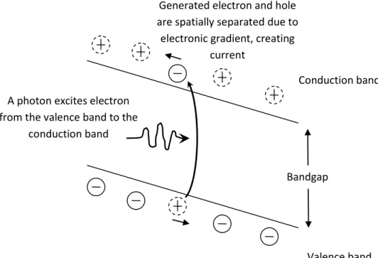
Upon exposure to light radiation, electrons in the cell’s light absorbing material are excited from the valence band (which consists of quantum states where the electrons are bound to the atoms) to the conduction band (which consists of quantum states where the electrons are free to move around). This process is often called the ‘electron-hole pair generation’, where free electrons are released from the atoms, leaving behind states which are not occupied by electrons (holes). By utilizing positively and negatively doped layers, an electric field is created inside the light absorbing material to separate the negatively charged electrons
21
from the positively charged holes. These charges are then collected by the electrodes of the cell. Some of these electron-hole pairs will recombine before reaching the electrode, a process commonly called the ‘electron-hole pair recombination’. The electron-hole pairs that do reach the electrodes will contribute to electric current, allowing us to extract electrical power from the solar cell (Figure 2.1.1).
The cell’s light absorbing material is commonly made from semiconductor. Different semiconductor materials have different electronic states, and consequently different energy bands and light absorption profile. Because of this, it is important to use materials with absorption profiles that overlap with the sunlight spectrum. Materials such as silicon, cadmium telluride (CdTe), and copper indium gallium selenite (CIGS) are commonly used for this purpose. Among these materials, silicon is widely used since it is abundant and cheap. However, the energy band structure of silicon is not ideal for solar cell due to the fact that the band gap is an
Conduction band
Valence band Bandgap
A photon excites electron from the valence band to the
conduction band
Generated electron and hole are spatially separated due to
electronic gradient, creating current
22
indirect band gap which makes silicon a poor light absorbing material. In order to mitigate this problem, various methods to improve light absorption (light trapping) are used in the cell such as increasing light scattering, reducing light reflection, employing back reflector, etc.
In this work, we focus our attention on a type of silicon solar cell called the thin film silicon cell. Unlike thick silicon cell which is made by cutting up silicon ingots, thin film silicon cells are made by depositing thin silicon layers in between other materials such as the Transparent Conducting Oxide (TCO), the metal back reflector, etc. Since thin film silicon solar cells use much less silicon (1-2 μm thick) than conventional thick silicon solar cell (a few hundred micron thick), thin film silicon cell costs less than conventional thick silicon cell, of which about 1/3 of the price is due to the material price of silicon. However, thin film silicon cell does not absorb light as efficiently as the conventional thick silicon cell due to the limited amount of light absorbing silicon. We will mitigate this problem by reducing incoming light reflection into the silicon cell by texturing the cell’s Transparent Conducting Oxide (TCO).
2.2 Transparent Conducting Oxide (TCO)
Ideally, the electron-hole pair generated by light absorption can directly be used for electricity. However, this is not the case and we have to extract the charge carriers (electrons and holes) using electrodes before we can use the electric current to generate power. We cannot simply use metal electrodes because they are not transparent, effectively blocking the sunlight from being able to enter the light absorbing silicon layer. It is necessary to use material which is transparent and conducting at the same time.
23
TCO thin films are used for this purpose. Since the band gap of the metal oxide is large enough, most of the light will not have enough energy to excite electrons from the valence band to the conduction band. In this case, light simply passes through the material as if it were transparent. In intrinsic form, the metal oxide is not conductive. However, by introducing doping in the metal oxide, we can create shallow donors near the conduction band (n-type) which allow electrons to be thermally excited into the conduction band, effectively making the transparent metal oxide conductive.
There are a few commonly used TCO such as tin-doped indium oxide (ITO), aluminum-doped zinc oxide (AZO), boron-aluminum-doped zinc oxide, and indium-aluminum-doped cadmium oxide [12]. Among these materials, ITO has the best performance as TCO due to its high conductivity. However, due to the fact that indium is a rare material, ITO is very expensive. On the other hand, zinc and alumina are both earth-abundant materials, making AZO an attractive alternative to ITO. In this work, we will be using Bosch’s boron-doped zinc oxide for our optical simulation. Bosch’s newly developed alumina-doped zinc oxide (AZO) will be used for our microtexturing experiment.
Simply using a flat zinc oxide (ZnO) layer as a TCO for thin film solar cell is not optimal, though. It has been found that by texturing the front TCO ZnO, incoming light into the silicon layer is scattered, increasing the light’s path length and electron-hole pair generation inside the light absorbing silicon layer, effectively improving light trapping and enhancing the electric current generated by the cell. Random texturing of ZnO can be obtained either by growing the oxide using Low Pressure Chemical Vapor Deposition (LPCVD) process or by wet etching using
24
hydrochloric acid (HCl). For both of these processes, there is a lack of texture geometry control, which is crucial for optimizing light trapping in the cell. In this work, we use optical simulation to optimize the geometry of the ZnO texture (Chapter 3), and explore an inexpensive method to fabricate it using nanosphere lithography (Chapter 4). We expect that the ZnO nanocone we obtain from this process will exhibit light scattering and wideband antireflection effect that improve light absorption in the thin film silicon cell over industrial standard HCl-etched ZnO.
2.3 Wideband Anti Reflection (AR) Effect of Periodic Nanostructure
Instead of relying on randomly textured ZnO to scatter light into the solar cell, we explore the possibility of using periodic nanostructure to improve light trapping and enhance absorption in the solar cell. The nanostructure is attractive because it exhibits the AR effect, which can be explained by the effective medium theory.
Effective medium theory is a physical model that approximates the macroscopic properties of a medium based on the properties and relative fractions of the materials composing the medium [13]. The theory is commonly used for properties such as electrical conductivity and dielectric constant. Since the dielectric constant ( ) and the refractive index (n) are related through the equation:
2
n
, (1)
it is common to use the effective medium theory to define the material’s effective refractive index (neff) and use it to analyze materials that are inhomogeneous at the sub-wavelength scale.
25
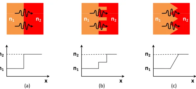
For two different dielectric materials with periodic nanostructure on their interface, the nanostructure can reduce light reflection by matching the effective refractive index between the two materials, as shown in Figure 2.3.1. For a nanostructure with tapered geometry, we can even achieve smooth and continuous transition of effective refractive index. Since this transition is experienced by any wavelength comparable to (or larger than) the nanostructure periodicity, tapered nanostructure can act as a wideband Anti-Reflection (AR) coating, unlike the conventional AR coating which is aimed at a specific wavelength. This wideband AR effect can potentially be useful for solar cell application, where the solar spectrum is spread across a wide spectrum of light.
It is not trivial to do an analytical study of this AR effect, especially when it comes to studying the tapered nanostructure geometry, which is expected to exhibit the best AR effect. In order to learn more about the AR effect, we have opted to do a simple Finite Difference Time Domain (FDTD) optical simulation instead. More details of our work on the optical simulation
n
1n
2n
1n
2n
1n
2n
1n
2x
n
1n
2x
n
1n
2x
(a) (b) (c)Figure 2.3.1: (a) step function change in index of refraction (b) slower index change due to sub-wavelength geometry (c) smooth index change due to sub-sub-wavelength tapered geometry
26
will be presented in Chapter 3. For the purpose of background knowledge on this wideband anti reflection effect, we created a simple 2-dimensional periodic nanostructure, as shown in Figure 2.3.2. Planar light propagates downward from an ideal material with refractive index of 1 to an ideal material with refractive index of 4. The total power of light transmitted through the interface is recorded and then integrated using an electric field monitor.
If the interface between the two materials is flat, the light transmittance across this interface is governed by the equation:
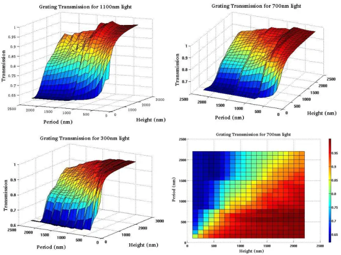
1 0.64 2 2 1 2 1 2 2 n n n n E E incident d transmitte . (2)For tapered nanostructure as shown in Figure 2.3.2, light reflectance can be greatly reduced, effectively increasing light transmittance into the cell. We varied both the nanostructure height and period from 100 nm to 2200 nm, and simulated transmittance across the grated interface
period height
n
1= 1
n
2= 4
E monitor Light source27
for light with 300-1100 nm wavelength. Some results from these optical simulations are shown in Figure 2.3.3.
It can be seen that the light transmittance of the nanostructured interface can be improved well over the light transmittance of the flat interface (0.64) when the nanostructure period becomes smaller and the nanostructure height becomes larger. Since this trend is observed for all of the simulated wavelengths, we can conclude that a tapered periodic nanostructure with appropriately tailored geometry can act as a wideband AR coating. This structure will be particularly useful for an interface with large change in refractive index since
28
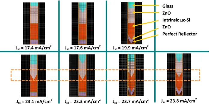
this interface is the largest source of light reflection out of the cell. In the context of a full single junction thin film µc-Si solar cell, this interface is between the front ZnO TCO (n~1.8) and the µc-Si layer (n~4). An indicator that this is indeed the case is shown using FDTD simulation result in Figure 2.3.4. A more thorough and detailed optical simulation about the implementation of this nanostructure in a solar cell will be presented in Chapter 3.
Jsc = 17.4 mA/cm2 Jsc = 17.6 mA/cm2 Jsc = 19.9 mA/cm2
Jsc = 23.1 mA/cm2 Jsc = 23.3 mA/cm2 Jsc = 23.7 mA/cm2 Jsc = 23.8 mA/cm2 Glass
ZnO
Intrinsic µc-Si ZnO
Perfect Reflector
Figure 2.3.4: Short circuit current (Jsc) obtained using FDTD simulation result for different grating structures. The simulations at the bottom row show that front TCO – µcSi interface matters the most in
30
Chapter 3 FDTD Optical Simulation to Enhance Light Trapping
3.1 Finite Difference Time Domain (FDTD) Optical Simulation
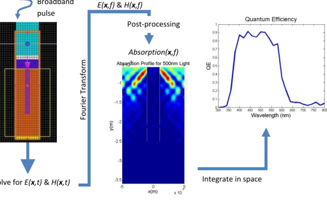
Finite Difference Time Domain (FDTD) is a simulation technique to solve electromagnetic field equations across a wide ride of frequency with a single simulation. It was first proposed by Kane Yee [14]. In this technique, we define a material structure in space and discretize the simulation space into xy coordinates (for 2D simulation) or xyz coordinates (for 3D structure). A short pulse of light is then propagated through the area of interest (simulation area) in the material structure. We discretize the time domain into small time steps and solve the light pulse propagation’s electromagnetic equation (Maxwell’s equations) for each time step in a leapfrog manner. In the beginning, the electric field components of the equations are determined for a specific time step. Afterwards, the magnetic field components are solved at the next time step. This process is repeated multiple times until the light propagation is completed and the electromagnetic field in the simulation area is below a certain threshold. After solving the light propagation in the time domain, we obtain the electromagnetic field profile as a function of space and time. Since a short light pulse in the time domain corresponds to a wide pulse in the frequency domain, we can perform Fourier transform on the electromagnetic field profile we have previously acquired, in order to obtain electromagnetic field profile as a function of space and frequency. Further processing of this frequency domain electromagnetic field spatial profile can be used to determine light absorption inside the structure. A brief summary of the FDTD method is shown in Figure 3.1.1.
31
The FDTD optical simulation method is advantageous since it can be used to solve electromagnetic equations, not only for planar structure (1D) but also for more complex 2D and 3D structures. It is also very useful since by solving Maxwell’s equations in one time domain simulation, we simultaneously solve the electromagnetic field profile in the material structure for a wide range of frequencies. Furthermore, it does not require manual parameter tuning since the only information that the method requires is the geometry of the material structure and the optical properties (n, k) of the materials involved in the simulation. The disadvantage of this method, however, is that it is very computationally expensive. For each simulation time step, it is necessary to record the time domain electromagnetic field spatial profile as well as to
Solve for E(x,t) & H(x,t)
E(x,f) & H(x,f) Absorption(x,f) Post-processing Fo u rier Tr an sfo rm Integrate in space Broadband pulse
32
Fourier transform this spatial profile for each frequency of interest. Therefore, a large amount of computation time and memory is required for the FDTD simulation.
3.2 μc-Si Solar Cell Model for Optical Simulation
It is important to estimate how much improvement we can achieve in a single junction μc-Si solar cell through light trapping. In order to do so, we used the FDTD technique to simulate the optical performance of single junction μc-Si cell. For the optical simulation portion of this work, we used a single junction microcrystalline silicon (μc-Si) cell structure developed by Bosch Solar Energy in 2010 (Figure 3.2.1). It has the following layer thicknesses:
1. Glass (SiO2) : 3 mm
2. Boron-doped Zinc Oxide (B:ZnO) : 1600 nm 3. p-type microcrystalline silicon (p-μcSi) : 10 nm 4. Intrinsic microcrystalline silicon (i-μcSi) : 1500 nm 5. n-type amorphous silicon (n-aSi) : 20 nm 6. Boron-doped Zinc Oxide (B:ZnO) : 400 nm
7. Perfect back reflector : 10 nm
Figure 3.2.1: FDTD model for a planar single junction μc-Si cell B:ZnO
i-μcSi B:ZnO Glass
33
The (n, k) data for each of the materials involved in this FDTD optical simulation is provided by Robert Bosch as well. Using these material data and layer thicknesses, we were able to construct the solar cell structure using Lumerical FDTD Solutions software.
3.3 QE and Jsc Extraction from the Simulated Solar Cell Structure
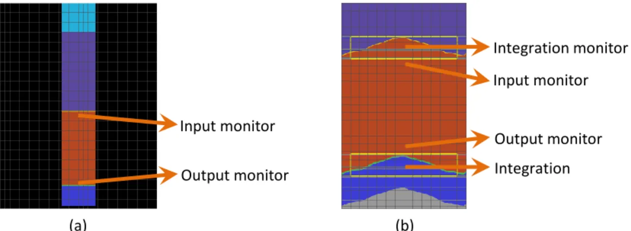
The FDTD optical simulation was constructed to study the light trapping efficiency of our solar cell structure. Since this work is focused on the optical performance of our cell, the most relevant parameter to be extracted using this optical simulation is the number of photons absorbed by the solar cell that can contribute to the generation of electron-hole pairs, which leads to the generation of electric current. In the case of our single junction μc-Si cell, only light absorption in the intrinsic μc-Si layer can contribute to this electric current. Since this is the case, we have to extract our absorption data carefully so that absorption in the other layers is not included in the calculation.
In the case of planar structure, this task can be done very easily. One can simply put an electric field monitor at the beginning and at the end of the layer of interest. In Figure 3.3.1(a) below, we put an electric monitor named ‘Input’ below the 10 nm p-type μc-Si layer and an electric field named ‘Output’ above the 20 nm n-type a-Si layer. These electric field monitors storeE ,
x f , which we can use to calculate the electromagnetic power P
f passing through the monitors. In this case, the electromagnetic power absorbed by the intrinsic μc-Si layer can simply be written as
f P
f P
f34
When we have to calculate light absorption in a textured solar cell (Figure 3.3.1(b)), the simulation setup becomes slightly more complicated. We can no longer use electromagnetic power passing through planar monitors to calculate electromagnetic power absorption since the interfaces between the different layers are no longer planar.
To fix this problem, we use rectangular 2D electric field monitors to record E
x,y,f
in the area around the textured interface. However, we need to be able to distinguish whether a certain
x,y coordinate is composed of intrinsic μc-Si or composed of another material. In order to do this, we put rectangular 2D refractive index monitors covering exactly the same area that the rectangular electric field monitors cover. The light absorption only in the intrinsic μc-Si can be found by integrating the electromagnetic power absorption from the coordinates where the refractive index in the coordinate is equal to the refractive index of intrinsic μc-Si. In pseudo-code, it means we perform the following operation:Input monitor Output monitor Input monitor Output monitor Integration monitor monitor Integration monitor monitor (a) (b)
35
for each frequency f:
f Pabs = 0for each x coordinate: for each y coordinate:
if n
x,y,f
== n
f of intrinsic μc-Si:
f P
f f dx dy E
x y f
n
x y f
Pabs abs * * * 2 , , *Im0* 2 , ,
where the last term in equation (4) corresponds to the electromagnetic power absorption in dy
dx * area on the simulation grid coordinates
x,y . Note that since this particular example is a 2D simulation, the absorbed power Pabs is represented in Watt/meter.At the end of this operation, we will obtain light absorption only in the intrinsic μc-Si within the monitor area. Combining the use of these 2D monitors with planar electric field monitors we have used previously will enable us to extract light absorption in the entire μc-Si layer. The absorbed power is dependent on the intensity of the incoming electromagnetic pulse we used in this FDTD simulation though, so it is much more useful to calculate the quantum efficiency (QE) instead, which is the actual optical characteristic of the solar cell. QE is a good standard for optical simulation since it ignores electron-hole recombination. For this FDTD optical simulation, the QE is obtained using the formula:
f P f P f QE pulse abs (4) (5)36
The QE curve is useful to show the spectral efficiency of our solar cell device. However, sometimes it is more convenient to describe solar cell performance by comparing single numbers instead of comparing different QE curves. The number of electron-hole pairs which the cell generates under standard 1 Sun light illumination (Figure 3.3.2) is a good choice for this purpose, as it reflects the optical efficiency of the solar cell. This number directly corresponds to the short circuit current density (Jsc) that the cell produces, which can be calculated using the formula:
q b E QE E dE
Jsc s *
where bs
E is the intensity of the solar spectrum for photon with energy E, and QE
E is the quantum photon conversion efficiency of the cell, in which we have ignored the electron-hole recombination effect. In the following sections, we will describe our solar cell’s optical performance using this short circuit current density Jsc.37
3.4 FDTD Simulation of μc-Si Cell with Different Textures
3.4.1 Flat Cell (Baseline)
Apart from the layer thicknesses and the material data, we need to take the light trapping geometry, which is the focus of this work, into account. In order to do so, we have prepared 3 different types of solar cell model using the same materials and layer thicknesses:
1. Planar single junction μc-Si cell (Section 3.3)
2. Single junction μc-Si cell with industrial HCl-etch textured ZnO (Section 3.4)
3. Single junction μc-Si cell with periodic submicron ZnO texture (Section 3.5 & 3.6)
The planar cell is used as the baseline, since theoretically this structure will have the lowest optical performance since it has no light scattering and anti-reflection mechanism. Our Lumerical FDTD simulation model for this cell is shown in Figure 3.2.1, and the resulting optical performance is shown in Figure 3.4.1.
Figure 3.4.1: QE curve of a flat single junction μc-Si Cell Jsc = 17.4 mA/cm2
38 3.4.2 Cell with Industry Standard LPCVD B:ZnO
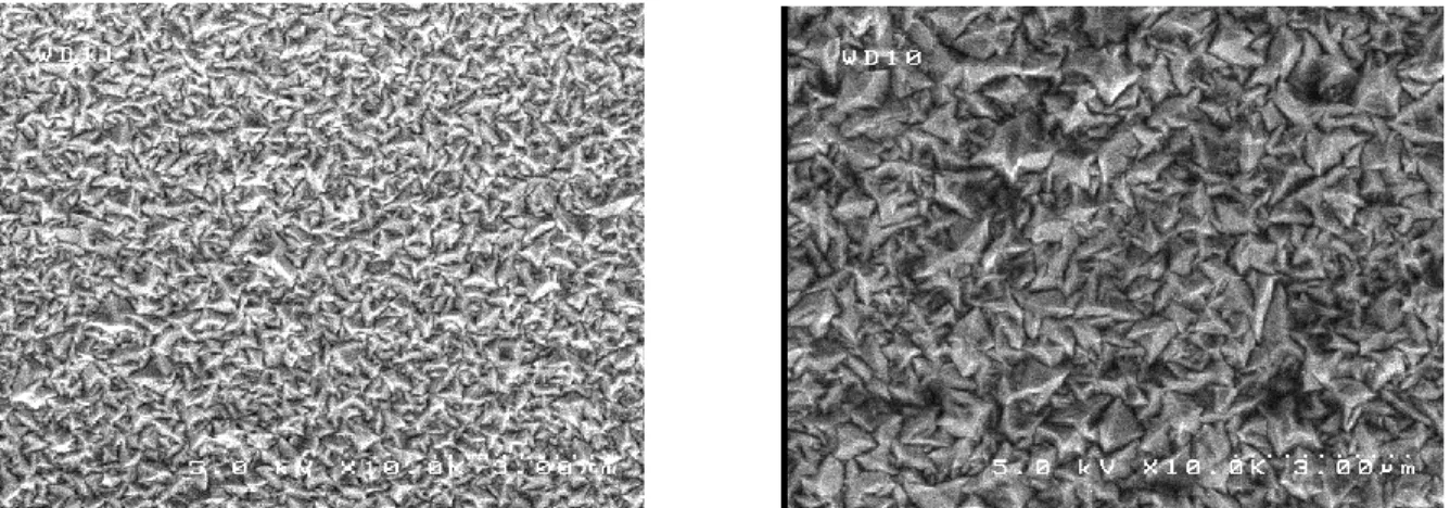
We would like to compare the optical performance of our submicron periodic ZnO texture not only to a planar single junction μc-Si cell, but also to a single junction μc-Si cell with industry standard textured ZnO. For the simulation part of this work, we worked with boron-doped ZnO that Bosch grows using Low Pressure Chemical Vapor Deposition (LPCVD) process. When B-doped ZnO is grown with this method, the surface of the ZnO is automatically randomly textured with feature size that increases with the thickness of the ZnO (Figure 3.4.2).
We are using Bosch’s 1600 nm B:ZnO for our FDTD simulation. The texture of this B:ZnO has previously been characterized by Bosch using Atomic Force Microscope (AFM). In Atomic Force Microscopy, a small cantilever with an even smaller tip on its end is used to physically trace the geometry of the sample. The sample deflects the cantilever and modifies the intensity of the laser beam that the cantilever reflects to the light detector, allowing the AFM to characterize the sample height using the cantilever deflection (Figure 3.4.3). The B:ZnO texture that Bosch obtained using the AFM is shown in Figure 3.4.4.
Figure 3.4.2: SEM image of 1500 nm thick B:ZnO texture (left) and 3000 nm thick B:ZnO (right) grown by Bosch. The texture feature size increases with film thickness.
39
To perform 2D FDTD simulation, we imported a texture line from the AFM characterization into our FDTD optical simulation model. For simplicity, we assumed that the rest of the material layers have the same texture as our B-doped ZnO. The FDTD optical simulation model for this structure and the resulting optical performance is shown in Figure 3.4.5. As we can see from the simulation result, randomly texturing the ZnO allows us to increase the cell’s Jsc from 17.4 mA/cm2 to 20.3 mA/cm2, a relative increase of 17 %. It can also be seen that our simulation result agrees very well with the experimental measurement obtained by Bosch.
Figure 3.4.3: AFM principle of operation [16].
40
3.4.3 Cell with Periodic 2D ZnO Texture
We propose that a ZnO textured with submicron periodic texture can provide optical enhancement to the solar performance when compared to an industry standard B:ZnO. The simplest way to test this hypothesis in a simulation would be to substitute each B:ZnO texture on our simulation model with a submicron periodic texture, similar to the optical simulation work performed in the references [17-18]. However, we would like to be able to test this hypothesis experimentally as well, which means we have to consider the way we make the submicron periodic texture on our ZnO. There is limited literature on methods to texture ZnO, and most texturing methods result in random feature size and aspect ratio. On the other hand, there are many known and controllable methods to texture silicon dioxide (SiO2), and it is most likely easier to deposit conformal ZnO on a textured SiO2 surface and obtain ZnO texture from such deposition. As such, we have opted to form our FDTD simulation by putting conformal layer of ZnO on textured SiO2 instead.
B:ZnO
B:ZnO i-μcSi Glass
Metal Reflector
Figure 3.4.5: FDTD simulation model and the resulting QE curve for single junction μc-Si cell with LPCVD B:ZnO texture. Simulated Jsc = 20.3 mA/cm2. Measured Jsc = 20.6 mA/cm2.
41 Glass B:ZnO i μc-Si B:ZnO Metal reflector
Figure 3.4.6: 2D FDTD simulation model for the triangular texture.
Glass B:ZnO
i μc-Si
B:ZnO Metal reflector
Figure 3.4.7: 2D FDTD simulation model for the sinusoidal texture.
Table 3.4.1: Jsc (mA/cm2) for triangular texture
Table 3.4.2: Jsc (mA/cm2) for sinusoidal texture
We used two different types of tapered geometry as our submicron periodic texture. The first one is a triangular texture, and the second one is a sinusoidal texture (Figure 3.4.6 and 3.4.7). Since the texture is periodic in the x-axis, the cell structure is periodic as well, allowing us to put periodic boundary conditions on the left and the right sides of the structure. We varied the period of the texture from 200-700 nm, and varied the height of the texture from 200-600 nm, and the resulting Jsc from this optical simulation are shown in the corresponding tables.
Height / Period (nm) 200 300 400 500 600 700 200 20.7 22.0 21.0 20.1 20.1 20.3 300 20.8 22.9 22.1 21.4 20.9 21.4 400 21.0 22.6 22.5 22.5 22.1 22.3 500 21.2 22.7 21.7 22.2 22.8 22.5 600 21.5 21.9 22.9 23.2 23.3 23.8 Height / Period (nm) 200 300 400 500 600 700 200 20.6 22.3 21.3 20.7 20.3 20.1 300 20.9 22.7 21.7 21.9 21.4 20.7 400 21.2 22.5 22.0 21.4 22.1 21.9 500 21.5 21.8 22.0 22.2 22.7 22.8 600 21.8 22.5 22.7 22.3 22.8 23.5
42
From this 2D optical simulation, two results can be observed:
1. Submicron periodic texture on ZnO does improve light trapping in μc-Si Cell, and there exist geometries that improve light absorption over random HCl-etched ZnO. For 2D texture with 600 nm height and 700 nm period we can achieve Jsc > 23 mA/cm2, compared to 20.5 mA/cm2 Jsc that a cell with industrial HCl-etched ZnO texture achieves.
2. The exact geometry of the tapered texture (triangle or sinusoidal) does not affect the submicron anti-reflection effect as much as the texture feature size does. This flexibility is important since fabricating perfectly sharp triangular glass texture might be considerably harder and more expensive than fabricating smoother texture.
3.4.4 Cell with Periodic 3D ZnO Texture
We further extended our FDTD optical simulation to three dimensional periodic textures. We believe the 3D version of our optical simulation is necessary since it is easier to manufacture 3D texture than 2D texture in an actual microfabrication. Furthermore, our initial attempts on 3D FDTD simulations indicated that the anti-reflection (AR) effect is strengthened when we use 3D texture instead of 2D texture for the same feature size.
To construct our 3D simulation structure, we followed the same procedure that we did in Section 3.4.3. We constructed a textured glass with periodic boundary condition and put conformal material layers on it to form the single junction μc-Si cell (Figure 3.4.8 (b)). Only light
43
absorption in the intrinsic μc-Si layer got included in the Jsc calculation. We attempted several other geometries as well in our 3D FDTD simulation (Figure 3.7.1 (c) and (d)).
Since 3D FDTD simulations require enormous amounts of computational resources, we had to limit our simulation to texture feature size that can potentially provide better AR effect. A few considerations were taken into account:
1. Initial work on AR effect (Section 2.3) indicates that 2D texture with small periodicity and large height provides the best AR effect. Increasing texture periodicity will reduce the AR effect slightly.
Figure 3.4.8: Usage of the periodic 3D texture in the µc-Si cell 3D FDTD simulation.
(a) (b) (c) (d) Glass B:ZnO i-µcSi B:ZnO Metal Reflector Glass Glass Glass
44
2. When the entire device structure is taken into account, 2D simulations (Table 3.4.1 and 3.4.2) seem to indicate that larger height and periodicity improve the light absorption more effectively.
3. It is easier to fabricate texture with large periodicity and height (low aspect ratio) rather than fabricating texture with small periodicity and large height (high aspect ratio).
Taking these considerations into account, we decided to focus on large periodicity and height as our simulation domain and limited our 3D FDTD simulation parameters to 600-900nm periodicity and 500-700nm height. The result of our 3D simulation is presented in Table 3.4.3 - 3.4.5. Height / Period (nm) 600 700 800 900 500 26.9 27.2 27.1 26.9 600 25.9 26.8 27.5 27.2 700 26.4 27.4 27.4 26.8 Height / Period (nm) 600 700 800 900 500 27.5 26.1 26.9 26.5 600 26.7 26.1 27.8 25.7 700 27.2 26.6 28.3 25.5 Height / Period (nm) 600 700 800 900 500 26.9 26.2 27.2 26.8 600 27.6 27.3 27.4 27.5 700 27.9 27.6 27.9 28.2 Table 3.4.3: Jsc (mA/cm2) for pyramidal texture
Table 3.4.5: Jsc (mA/cm2) for 3D sinusoidal texture Table 3.4.4: Jsc (mA/cm2) for inverted pyramidal texture
45
It has to be noted that due to limited computational resources, we were using lower accuracy setting to complete these 3D simulations. Because of this, the Jsc is overestimated by 1-2 mA/cm2 for each of these simulations. Nevertheless, it can be seen that ZnO with 3D submicron periodic texture can enhance Jsc in our single junction μc-Si cell up to 25-26 mA/cm2, a 25-30% relative increase in light absorption over industrial HCl-etched ZnO texture which only provides a Jsc of 20.5 mA/cm2. Figure 3.4.9 compares the simulated quantum efficiency (QE) between different ZnO textures (assuming perfect carrier collection), showing that the improvement is seen over a large range of wavelengths. As mentioned in Section 2.3, we believe this broadband increase in QE is caused by the submicron texture’s anti-reflection effect.
Figure 3.4.9: Simulated QE of different ZnO textures. Both the 2D and 3D periodic ZnO textures have 600 nm periodicity and 700 nm height.
47
Chapter 4 ZnO Nanocone Microfabrication
As we have mentioned in chapter 3, random texturing of ZnO is quite a well-known process; B:ZnO deposited using LPCVD ends up being textured on its own, while aluminum-doped ZnO (Al:ZnO) can be chemically textured using dilute hydrochloric acid (HCl). However, to the best of the author’s knowledge a method to control periodic texturing of ZnO over large substrate has not been thoroughly explored. On the other hand, there are many known methods to texture glass (SiO2). Since in this experimental section we work with Al:ZnO deposited by Bosch, we have opted to put periodic submicron texture on the glass surface instead. Conformal layer of Al:ZnO will then be deposited on top of the textured glass to obtain our textured ZnO.
The goal of our experimental work is to achieve periodic ZnO structure with 800-900 nm periodicity and 700-800 nm height. The following are the challenges addressed by this work:
1. The standard industry process (random texturing of ZnO using HCl) is not usable because we would like to control ZnO texture periodicity and height.
2. The texturing process is preferably cheap and scalable so that it can be incorporated into solar panel production if the experimental result is promising.
3. The glass texture has to be sharper than 800 nm since ZnO deposition on textured glass will result in duller ZnO texture.
4. The ZnO texture needs to be of a tapered geometry (nanocone or nanopyramid are preferred while nanopillar is undesired).
48
4.1 Colloidal Lithography
The approach that we found to be the best for our goal of controlling texture periodicity and height is colloidal lithography. Colloidal lithography is a method to make nanopattern using closely packed microsphere as the mask. In this technique, we self-assemble a closely packed microsphere monolayer in hexagonal pattern using Langmuir-Blodgett deposition method on the glass surface. This microsphere mask is then used as the etching mask for glass (SiO2) dry etching process using CHF3 and O2. Our process is similar to the process developed by Hsu et al. [19], but different microsphere mask and substrate materials are being used for our purpose. Before we go into the details of our process in the following sections, a brief review of Langmuir-Blodgett deposition and dry etching will be useful.
4.1.1 Langmuir-Blodgett (LB) Deposition
In this deposition technique, functionalized microspheres with polar and non-polar parts are released into the surface of a liquid (water in our case). Since the non-polar tail on the microsphere tends to stay away from the polar water molecules, the particles do not sink into the water when they are gently injected into the water surface (Figure 4.1.1). Various types of particles have been deposited using LB deposition [19-21], further emphasizing the robustness of this technique. These microspheres are then gently compressed using a barrier, forcing them to form a closely packed microsphere monolayer on the water surface. Once the monolayer is formed, the substrate is immersed and then pulled out of the water surface, effectively pulling away the particles from the water and transferring them to the substrate’s surface (Figure 4.1.2).
49
Figure 4.1.1: (a) Functionalized microspheres aligned on the water surface [22], (b) Langmuir-Blodgett deposition process using LB trough [23].
Figure 4.1.2: Langmuir-Blodgett KSV 5000 system that we used in Stanford Soft and Hybrid Materials Facility (SMF) for LB deposition.
(a)
50 4.1.2 Dry etching
The dry etching process is also commonly called the Reactive Ion Etching (RIE). In this process, we use a strong electric field to ionize chemical gas and accelerate the ions generated by the electric field to the substrate. Since these ions are accelerated with high energy, they chemically react with the substrate more easily and etch the substrate material away. The rate of chemical reaction depends on various process parameters and the type of material being etched away. When this RIE process is applied to our microsphere-masked substrate, it is possible to control the dimension of the substrate texture after the etching process, as shown in Figure 4.1.3. The texture periodicity is strictly determined by the microsphere mask diameter. On the other hand, the shape and sharpness of the texture is determined by the process parameters and the materials that we use.
4.2 Colloidal Lithography on Quartz Wafer with Silica Microsphere Mask
Hsu et al. [19] have previously functionalized silica (SiO2) microspheres using 3-aminopropyltriethoxysilane (APTES) and have used Langmuir-Blodgett (LB) deposition to self-assemble the spheres in hexagonal pattern on a silicon wafer. They have also shown that the
Accelerated ion
Glass (SiO2) Glass (SiO2) Glass (SiO2)
Figure 4.1.3: Controlled destruction of the microsphere mask and the substrate material during RIE allows us to control the resulting texture dimension.
51
silica spheres form a good mask to do RIE on silicon. We begin our effort on colloidal lithography by performing LB deposition of silica microspheres on our glass substrate. Our goal is to have ZnO nanocone texture with ~800 nm periodicity and ~800 nm height, so we need to have glass texture with taller nanocones, preferably larger than 1 µm in height.
4.2.1 Silica Microsphere Functionalization and LB Deposition
We purchased silica microsphere with 750 nm diameter in powder form from Fiber Optic Center and purchased APTES from Sigma-Aldrich. Based on Hsu’s work as the starting recipe [19], we performed APTES functionalization on our silica microspheres.
We dispersed 160 mg of these microspheres in 30 mL of ethanol and ultrasonicated the colloidal solution in order to segregate the microspheres. We then added 4 mL deionized (DI) water and 0.4 mL APTES into the solution. We needed the APTES to be uniformly distributed in the solution, so we stirred the solution for 8-12 hours. We then heated the solution at 100o C for 3 hours while continuing to stir it. This heating step is important since APTES functionalization is a temperature activated process. After the heating process, we cleaned the solution by centrifuging in ethanol three times. Methanol should then be used as the final solvent in the solution. We find that a silica microsphere solution with a concentration of 10 g/L is ideal for our LB deposition. Typically, we used 8 mL of our microsphere solution in one LB deposition session, which is enough to coat four 4” wafers. As explained in Section 4.1.1, after this functionalization the spheres are capable of staying afloat when injected slowly into the water surface.
52
To perform our Langmuir-Blodgett deposition, we used the KSV 5000 LB trough from KSV NIMA. This tool is available in Stanford Soft and Hybrid Materials Facility (SMF), and it is essentially a water bath with compression barriers made from hydrophobic material. We started the LB procedure by cleaning the trough thoroughly to remove contaminants from previous tool users. Then, we overfilled the bath with water and injected our microsphere solution into the surface at a constant rate of 5 mL/hour. The tool setup is shown in Figure 4.2.1.
Water bath
Automatic injector Syringe + Teflon tube
Figure 4.2.1: LB trough setup. The top picture shows the trough and the compression barrier. The bottom picture shows the microsphere injection setup.
SP monitor
Compression barrier
53
When the microspheres were injected into the water surface, they were not closely packed yet. The microspheres were spread across the water surface and they needed to be compressed using the compression barrier until a closely packed microsphere monolayer was formed on the water surface. To find out when this condition happened, we monitored the water Surface Pressure (SP) using a sensor, which in this case is simply a piece of paper suspended on a spring-loaded microbalance (Figure 4.2.2). When the surface pressure increased exponentially with respect to compression barrier position, we know that the microspheres were closely packed. When this happened, we immediately stopped the barrier compression and started dipping our glass substrate into the water. Since the subsequent dry etch process requires the use of low-impurity substrate, we used quartz wafer as our substrate (high purity SiO2). We dipped 2 wafers back-to-back at once, allowing us to deposit closely packed microspheres on two wafer surfaces at once.
SP sensor Closely packed silica microspheres
Quartz wafer
Dipper
Figure 4.2.2: The LB trough operation once the microspheres are closely packed. We transfer the spheres from the water to the wafer by dipping the wafer into the water and pulling it out slowly.
54
When we pulled the two wafers slowly out of the water, the microspheres were transferred from the water to the wafer. When this happened, the number of microspheres on the water surface was reduced and the SP decreased since the microspheres were no longer closely packed. To mitigate this problem, during the pulling out process we compensated for the reduced number of spheres by pushing the compression barriers closer together. The compression barrier movement during the pulling out process was controlled with the feedback signal from the SP measurement, and a typical barrier movement and SP measurement are shown in Figure 4.2.3.
After the wafers have been completely pulled out of the water, the wafers were fully covered with 750 nm closely packed silica microspheres. A few Scanning Electron Microscope (SEM) images of these microspheres are shown in Figure 4.2.4.
Figure 4.2.3: Barrier position (blue line) is controlled to keep the SP (green line) as constant as possible during the pulling out process.
55
4.2.2 Dry Etching of Quartz with Silica Microsphere Mask
After we had confirmed that we obtained a closely packed silica microsphere monolayer using LB deposition, we proceeded to the dry etching process. Since we are etching a quartz (SiO2) wafer, we need to use a dry etching process that is designed to etch SiO2. We do this etching process in Stanford nanofabrication Facility (SNF) using the tool AMT 8100 Plasma Etcher. To avoid contaminating the tool with impurity from regular glass, we use quartz for our
(a)
(b)
(d)
(c)
Figure 4.2.4: (a) Silica microspheres coating almost the entire wafer. (b) SEM image of the interface between coated and uncoated wafer surface. We can clearly see that there is only a monolayer of microspheres. (c) The microspheres are very closely packed. (d) The defect in the
56
substrate; this is the reason we chose quartz substrate instead of regular glass. For this dry etch process, we define 1 etching cycle as:
1. SiO2 etch using 85sccm CHF3 and 6sccm O2 plasma for 15 minutes. 2. De-scum CHF3 polymer residue using 50sccm O2 plasma for 5 minutes.
We inspect our samples under the SEM after a few etching cycles, and the images of the resulting quartz textures are shown in Figure 4.2.5.
After 3 etching cycles, the silica microspheres were completely etched away. Increasing the number of etch cycles would simply destroy and dull the textured quartz, so we concluded that we could only obtain 450-500 nm texture on quartz using silica microspheres as the etching mask. This is insufficient for our goal of obtaining 1 µm sharp nanocone on our quartz
(a)
(b)
(c)
Figure 4.2.5: Top-down and cross-section SEM images of our quartz texture after LB deposition of silica microsphere and dry etching for (a) 1 cycle, (b) 2 cycles, and (c) 3 cycles respectively.
57
substrate. Nevertheless, it is interesting to learn how conformal Al:ZnO can be deposited on this glass texture.
4.2.3 ZnO Deposition on Silica-Masked Quartz Nanocone
We sent the quartz wafer with 3 etching cycles (Figure 4.2.5(c)) to Bosch Corporate Research (CR) in Germany for Al:ZnO deposition on the top of our quartz texture. We chose 800 nm Al:ZnO thickness since it was the standard ZnO thickness that Bosch CR used in 2011. The Al:ZnO deposition was done using Physical Vapor Deposition (PVD). We characterized the resulting ZnO texture as shown on Figure 4.2.6.
Figure 4.2.6: (a) & (b) Top down view of the ZnO texture. (c) Cross section view when 800 nm Al:ZnO is deposited on non-textured quartz. The process normally generates flat ZnO. (d) Cross
section view when 800 nm Al:ZnO is deposited on our quartz nanocone.
Quartz Al:ZnO Quartz Al:ZnO
(a)
(b)
(c)
(d)
58
As we can see in Figure 4.2.6, 800 nm Al:ZnO deposition on textured quartz produced a ZnO texture with gaps in between. This happened because the sputtered Al:ZnO was not capable of perfectly filling the gaps between the quartz nanocones. This problem can possibly be mitigated by using a lower pressure during the PVD process, but it involves process parameter tuning on the PVD tool in Germany and is not pursued in this work. Instead, we focus on key aspects that can be learned from the enlarged ZnO texture image (Figure 4.2.7):
1. 800 nm thick ZnO reduces the nanocone texture height. We have 450 nm nanocone on the quartz, but only 200 nm nanocone after the ZnO deposition.
2. The gap formation in the ZnO has to be avoided since the ZnO needs to be an electrical conductor. Charge carriers will not be able to move freely through the gaps; they most likely move through the 200 nm conformal layer on the bottom instead.
Figure 4.2.7: 800 nm Al:ZnO on quartz nanocone with 750 nm periodicity, 450 nm height. 750 nm
200 nm
450 nm 200 nm
59
We expect that these problems can be mitigated by fabricating a sharper quartz nanocone texture and reducing the Al:ZnO thickness. However, we are limited to 450 nm quartz nanocone height if we use the silica microspheres as our etching mask. Because of that, we need to use microspheres made from a material that will be more resistant to SiO2 dry etch.
4.3 Colloidal Lithography on Quartz Wafer with Polystyrene Microsphere Mask
Photoresist is very commonly used as an etching mask in semiconductor microfabrication. Since photoresist is essentially a polymer, we believe that microspheres made from a polymer will be similarly resistant to our oxide Reactive Ion Etching (RIE) process. For this reason, we choose polystyrene microspheres as our etching mask since they are quite common and available commercially. Furthermore, there has been some prior work on the usage of polystyrene microspheres in the LB deposition, strengthening our confidence that polystyrene microspheres are ideal for our process [24-26].
We started our polystyrene microsphere LB deposition by purchasing amine-functionalized polystyrene microspheres with 750 nm diameter from Polysciences. The reasoning behind this decision is the fact that we functionalized the surface of our silica microspheres with the APTES’ amine group for our LB deposition in section 4.2 [27]. However, after numerous trials we concluded that the amine-functionalized polystyrene microspheres are not suitable for LB deposition. Most of these spheres sank into the water during the sphere injection and barrier compression phase. The SEM image from our LB deposition using these spheres is shown in Figure 4.3.1.
60
We also took a different approach by attempting to use non-functionalized polystyrene microspheres with 750 nm diameter purchased from Polysciences. The reason behind this attempt is that none of the prior works on polystyrene LB deposition that we have studied mentions the need for surface functionalization. This approach seemed to work better because we could clearly see that the non-functionalized microspheres floated on the water surface and were transferred to the quartz wafer using LB deposition. However, these microspheres aggregated too easily. They tended to stick and bond with one another, so a periodic and closely packed microsphere monolayer could not be obtained. We were unable to mitigate this problem even after thoroughly ultrasonicating the microsphere solution and functionalizing the microspheres with APTES, as we did on the silica microspheres. Figure 4.3.1 shows the polystyrene microsphere layer that we obtained after the LB deposition using the polystyrene spheres.
Figure 4.3.1: Polystyrene microspheres deposited on our substrate using LB method. The left image is that of amine-functionalized spheres with most of the spheres sinking into the water. The
right image is that of non-functionalized spheres modified with APTES, showing sphere aggregation. As received, non-functionalized spheres behave similarly.
61
After these attempts, we concluded that the polystyrene microspheres that we commercially had access to did not possess microsphere surface properties that are suitable for our LB deposition process.
4.4 Colloidal Lithography on Quartz Wafer with Hybrid Microsphere Mask
In Section 4.1, we found that silica microspheres have a surface property that is suitable for the LB deposition. After APTES functionalization, these spheres float on the water and can form a closely packed microsphere monolayer. However, silica is not resistant to oxide etch and the quartz texture that we obtain is not sharp enough. On the other hand, we have polystyrene microspheres which are most likely resistant to oxide etch. However, in Section 4.3 we found that it is very challenging to obtain a microsphere monolayer using polystyrene microspheres since the surface property of these spheres is not suitable for LB deposition. It is desirable to have a microsphere whose surface is compatible with LB deposition but is resistant to oxide etch as well. Because of that fact, we set out to create a hybrid microsphere made from a polystyrene core and a thin silica shell.
4.4.1 Synthesis of Polystyrene-Silica Hybrid Microsphere
Graf et al. have developed a robust method to coat polystyrene microspheres and various other particles with thin silica shells [28]. In their method, polystyrene microspheres are first coated with polyvinylpyrrolidone (PVP). When the PVP-coated microspheres are immersed in an ethanol solution containing ammonium hydroxide (NH4OH) and tetraethyl orthosilicate (TEOS), PVP acts as the layer which facilitates the growth of thin silica shells on the microspheres. For our process, we used a solution of 750 nm non-functionalized polystyrene

![Figure 3.3.2: ASTM G173-03 Reference Spectra [15]](https://thumb-eu.123doks.com/thumbv2/123doknet/14017799.457099/36.918.170.756.715.1018/figure-astm-g-reference-spectra.webp)