Analysis, Synthesis, and Fabrication of VLSI Si
Detector Arrays for Optoelectronic
Interconnections
by
Edward Joseph Ouellette III
Submitted to the Department of Electrical Engineering and
Computer Science
in partial fulfillment of the requirements for the degrees of
Bachelor of Science
and
Master of Science
at the
MASSACHUSETTS INSTITUTE OF TECHNOLOGY
May 1994
) Edward Joseph Ouellette III, MCMXCIV. All rights reserved.
The author hereby grants to MIT permission to reproduce and distribute publicly paper and electronic copies of this thesis document in whole or in part, and to grant
others the right to do so.
Author ... ... . .-.... a. ...
Deptme of Electrical Engin ejng and Conputer cience
/.( // / YIay1 , 1994
Certified by ... .. .
..
. ... .., A / Thomas. Knight
7'J
,/ /t
~
Thesis
Supervisor
(Academic)
Certified
by....
... '...
...
Alan Huang /nFpfpany pXrv sor (AT&T Bell Laboratories) A ccnt.Pl hv-JUL L I'f
rrederic ft. vlorgentnaler
Committee on Graduate Students
JTE
MIT L,8RA't]'
Analysis, Synthesis, and Fabrication of VLSI Si Detector
Arrays for Optoelectronic Interconnections
by
Edward Joseph Ouellette III
Submitted to the Department of Electrical Engineering and Computer Science on May 6, 1994, in partial fulfillment of the
requirements for the degrees of Bachelor of Science
and
Master of Science
Abstract
Optics possesses many benefits over electronics for high-speed interconnections. Fur-thermore, the reliability and affordability of current Si CMOS VLSI technologies over other heterogeneous technologies, such as GaAs, suggests that Si optoelectronic mi-crosystems can be a viable, low-cost solution to high-speed interconnect problems. This thesis focuses on the receiver end of optoelectronic interconnects, and more specifically addresses the issues of optimal Si photodetector design within the con-straints of an unmodified CMOS VLSI technology.
Various photosensors are compatible with a standard Si CMOS VLSI process. The simple graded-junction N+N/P diode was shown to have the best optical and electrical performance of all the types investigated, hence, it was used as a template for a photodetector analysis, synthesis and parasitic extraction CAD tool. A fabricated Si photodetector array in a standard AT&T CMOS process had 0.56 A/W responsivity at 850 nm wavelengths with only 2.5V of reverse bias; the device capacitance was 70 pF/mm 2, and the dark current was 61 nA/mm2, in agreement with simulations.
A new CAD tool was written to address the need for computer automation in the area of photodetector design and analysis. The tool provides analysis and opti-mization of photodiode parameters, synthesis of photodetector array mask geometries (including array wiring) for several photodiode styles, and parasitic model extraction for SPICE simulations. It is both process-technology and hardware-platform
inde-pendent allowing portability. Moreover, the output format is compatible with the
MOSIS shuttle service, aiding in quick, inexpensive turn-arounds of optoelectronic designs.
Thesis Supervisor (Academic): Thomas F. Knight
Title: Principle Research Scientist: Electrical Engineering and Computer Science Thesis Supervisor (AT&T Bell Laboratories): Alan Huang
Acknowledgments
Alan Huang provided much inspiration, support, and personal encouragement with this thesis and has been a constant friend. Tom Knight also helped me think of fun-damental concepts in a new light (excuse the pun). Thank God for creative thinkers! Jay O'Neill provided extensive MULGA support, and has been a humorous (R.P. supporter) friend through difficult times. Ted Woodward assisted in the optical setup experiments; Jim Walker helped with fabrication techniques and taught me how to use a wire-bonding machine- a skill to add to my resume (not!)
Sam Reynolds at MOSIS provided the MOSIS Scalable CMOS Design Rule files presented in Appendix C.
To my freshman advisor and long-time friend, Hugh Secker-Walker, thanks for all the wonderful discussions. Also, many thanks to Fr. Dave, Fr. Campbell, and Tom Hereford- three wonderful spiritual advisors who have had a great influence on my
life.
To the many wonderful friends in LAG, especially Derek and Lisa, who have provided me with extra spiritual impetus to realize my dreams - my heart goes out to you.
Thanks also to Brian, Kent, Ochida, and Steve who have always been special friends. To Bob and Susan, for years of constant support and encouragement, sense-less humor, and for being great "parents away from home" - I love ya!
Extra thanks goes out to J.C. for helping me persist with this thesis even through
extenuating circumstances. First, half-way into my research completely new research had to be started after my original advisor left AT&T to found a company. Second, departmental funding constraints limited fabricating only a few, simple chips through the AT&T shuttle. Finally, upon my return to MIT, the entire AT&T tool suite had to be ported to my home computer in order to finish the CAD tool design.
To Michelle and Grant - thanks for the "home away from home," for the great meals and excellent company. Extra special thanks go out to my family for their love, support and encouragement. Thanks, Dad, for helping to bring out the scientist in
me and for all the mechanics training! Mom, I'll never forget your comment to me that you once felt like the Pope speaking to Michelangelo when he was painting the Sistine Chapel: "it's been long enough - just get the thing finished!"
Contents
1 Introduction
1.1 Overview. ...
1.2 The Need for Optical Interconnect Systems ...
1.3 Thesis Outline .
2 The Advantages of Optics
2.1 Overview . ...
2.2 Wiring Density. 2.3 Available Bandwidth.
2.4 Attenuation Factors .
2.5 Fanin and Fanout Limitations
2.6 Impedance Mismatch Noise 2.7 Switching Noise. 2.8 Crosstalk Noise. 2.9 EMI Immunity. 2.10 Mutability of Connections 2.11 Reliability Concerns ... 2.12 Communication Energy . 3 Si Optical Sensors 3.1 Overview ... 3.2 Photosensor Types. 3.2.1 Photoconductor. 15 15 16 17 19 19 20 20 23 24 25 26 27 28 28 29 30 35 35 36 37
3.2.2 Photodiode 3.2.3 Phototransistor 3.3 Important Photodiode Pa 3.3.1 Active Area 3.3.2 Breakdown Voltag 3.3.3 Capacitance . . . 3.3.4 3.3.5 3.3.6 3.3.7 3.3.8 3.3.9 3.3.10 3.3.11 3.3.12 3.3.13
Crosstalk (for arra
Dark Current . . Detectivity Noise . Quantum Efficienc Response Linearity Response Uniform Responsivity . Response Speed . Series Resistance rameters . e (reverse bias) ys) ity . . . . . . . . . . . 3.3.14 Shunt Resistance
3.4 Monolithic VLSI Photodetector Designs
3.4.1 Monolithic Photodetector Geometry Examples
4 Photodetector CAD Tool Design
4.1 Overview .
4.2 CMOS VLSI Photodetector Design Tradeoffs . 4.2.1 Responsivity Versus Bandwidth
4.2.2 Responsivity Versus Process Complexity 4.2.3 Geometry Versus Responsivity and Noise 4.2.4 Geometry Versus Responsivity and Series 4.3 MULGA: AT&T's VLSI CAD tool set ...
4.3.1 Cell Design Loop ... 4.3.2 Module Design Loop ...
. . . .. . .. ... ·.... . . . . . . . .. .
Resistance
...
. . . .. . . . .,. . . . . .. .. . . .... . 41
. .... .... . .. ... .
.43
. . . 43 . .... .. .. . .. ... . .. 44. .... .... . .. ... .
.45
. .... .... . .. . .. . .47 . . .. . .... ... ... . .48 . .... .. .. . .. ... . .49 . .... .. .. ... ... . .. 49 . . . 51 . . . 55 . . . 56 . . . 56 . . . 58 . . . 61 . . . 61 . . . 61 64 71 71 72 72 73 74 74 74 75 77 ... 374.3.3 Limitations of MULGA .
4.4 Photogen - A Photosensor CAD Tool ...
4.4.1 Required Features of a Photodetector CAD 4.4.2 Integration into Commercial CAD Systems
4.4.3 Internal Database Format ...
4.4.4 MOSIS Compliance ...
4.4.5 Operation ...
4.4.6 Layout Synthesis Algorithms .
4.4.7 Parasitic Extraction Algorithms ...
. .. . Tool .. . .. . . . . . . . . . . 5 Results
5.1 MULGA Mask Files.
5.2 Fabrication and Bonding .. ... .... ...
5.3 Optical and Electrical Measurements ...
6 Conclusions and Future Research
6.1 Overview .
6.2 Conclusions ... 6.3 Future Work ...
6.3.1 Fabrication ...
6.3.2 Process Modifications . ... 6.3.3 CAD Tool Enhancements ...
A Derivations of Photodiode Equations
A.1 PN Abrupt-Junction Photodiode ... A.1.1 Carrier Concentrations.
A.1.2 Charge Density.
A.1.3 Electric Field Intensity ...
A.1.4 Potential Distribution.
A.1.5 Depletion Width. A.1.6 Depletion Capacitance.
78 80 80 81 82 84 84 87 89 91 92 94 95 101 101 102 102 103 103 103 105 105 106 106 108 109 111 112 . . . . . . . . . . . . . . . . . . . . . . . . . . . . . . . . . . . .
A.2 PN Linearly-Graded Junction Photodiode A.2.1 Charge Density.
A.2.2 Electric Field Intensity ...
A.2.3 Potential Distribution.
A.2.4 Depletion Width. A.2.5 Depletion Capacitance. A.3 PIN photodiode ...
... . . . 113 ... . . . 113 ... . . . 114 ... . . . 115 ... . . . 116 ... . . . 117 ... . . . 117
B Important Photodiode Parameters
C MOSIS SCMOS Design Rules
119 121 . . . . . . . . . . . . . . . . . . . .
List of Figures
2-1 Time Division Multiplexing of Optical Interconnects ... 21
2-2 Parallel Optoelectronic Interconnect Links ... 22
2-3 Attenuation of Optical and Electrical Interconnections ... 24
2-4 Integrated Optical Imaging System ... 26
2-5 Synchronous Optical Clock Distribution ... 27
2-6 Series-Terminated Electrical Transmission Line ... 31
2-7 Free-Space Optical Communication Link ... 32
2-8 Communication Energy Versus Distance ... 33
Photodetector Types ... General Photodiode Circuit Model ... Photocurrent-mode, Photodiode Model ... Schottky MSM Photodiode ... Photodiode Junction Diffusion Structures ... Absorption Coefficient Versus Wavelength for Various Mate Spectral Responsivity of a Typical Silicon Photodiode . . . AT&T CMOS Process-Compliant Si Photodiodes ... Simple N+N/P Rectangular Photodetector Geometry . . . N+N/P Interdigitated Finger Photodetector Geometry I N+N/P Interdigitated Finger Photodetector Geometry II . N+N/P 1-D (1X4) Photodetector Arrays ... I
... .. 36
... . .38
... . .40
... . .41
... . .44
ials . . . 54... . .58
... . .62
... . .65
... . .66
... . .67
... . .69
4-1 Cell Design Loop ... 4-2 Module Design Loop ...
75 76 3-1 3-2 3-3 3-4 3-5 3-6 3-7 3-8 3-9 3-10 3-11 3-12
4-3 MULGA Directory Tree
4-4 MULGA Mask Format Interconversions ... 79
4-5 Photogen Process Flow ... 85
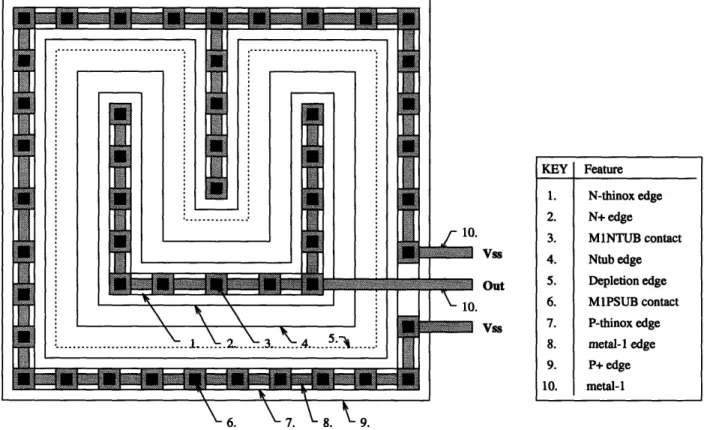
4-6 Mask Contact Types for N-well Process ... 88
4-7 1-D (1x8) Wired Photodetector Array ... 89
4-8 2-D (4x8) Wired Photodetector Array ... 90
5-1 AT&T GaAs Microlaser Array ... 91
5-2 Medit View of Photodetector Array Top Levels ... 92
5-3 Medit View of Entire Photodetector Array ... 93
5-4 Closeup of Photodetector Array. ... 94
5-5 AT&T 0.9/um CMOS Photodetector Array ... 95
5-6 AT&T 0.9,/m CMOS Photodetector Array Bonding ... 96
5-7 AT&T 0.9/lm CMOS Photodetector Array Pads ... 97
A-1 Step-Junction PN Diode Carrier Concentrations ... 106
A-2 Step-Junction PN Diode Charge Density Distribution ... 107
A-3 Step-Junction PN Diode Electric Field Distribution ... 109
A-4 Step-Junction PN Diode Potential Distribution ... 111
A-5 Linear-graded PN Diode Carrier Concentration ... 113
A-6 Linear-graded PN Diode Charge Density Distribution ... 113
A-7 Linear-Graded PN Diode Electric Field Distribution ... 114
A-8 PIN Diode Characteristic Distributions ... 118
List of Tables
3.1 Characteristics of CMOS-compatible Photodiodes . . . 63
5.1 Neutral Density Filter Powers ... 96
5.2 Photodiode Surface Edge-Junction Response for OV bias ... 98
5.3 Photodiode Center (Tub) Response for OV bias . ... 98
5.4 Photodiode Surface Edge-Junction Response for 2.5V reverse bias . 99 5.5 Photodiode Center (Tub) Response for 2.5V reverse bias ... 99
Chapter 1
Introduction
1.1 Overview
The Digital Optics Group at AT&T Bell Laboratories in Holmdel, New Jersey has been investigating low-cost, massively parallel monolithic optoelectronic interconnect microsystems, specifically developing Optical Data Link (ODL) ICs, using an in-house Si CMOS VLSI process technology [AD88, DPC+89]. Previous systems achieved very low communication rates (under 10 Mb/s per channel) - an order of
magni-tude slower than expected through simulation results -, and the cause for the low
throughput has yet to be explored. We believe that a system redesign will yield much more interesting results. CAD tool deficiencies in the area of modeling OEIC designs were flagged as the downfall in the first design.
The standard AT&T VLSI design tool package, MULGA, [ACW87] uses symbolic mask editing for custom layouts, and cannot easily adapt to handle photodetector devices nor parasitic extraction of such geometries, nor the creation of accurate mod-els for simulation. Other commercial CAD tools suffer the same deficiency: there is clearly a need for new CAD tools in the area of custom optoelectronic devices that in-terface cleanly with existing VLSI CAD packages, such as MULGA [McB90, Rub90Ob]. Moreover, in such a CAD package, many issues such as mechanical alignment, quan-tum efficiencies, transit response times, geometries of photodetectors, and receiver noise and sensitivity have yet to be addressed accurately.
The goals of this thesis are to further investigate several possible photodetector styles and geometries compatible with a standard AT&T Si VLSI CMOS process and to develop new CAD tools to aid in the design, analysis and synthesis of such devices for easy integration into receiver amplifier designs. A new photosensor CAD tool integrated into the MULGA package should allow designers to input required photodetector parameters such as area, response time, geometric configuration, light factors, and have complete mask specifications and accurate simulation models gen-erated without having to rely on back-of-the-envelope calculations and hand layout of intricate detector mask geometries. Moreover, the tool developed will be designed for process-independence so that the standard MOSIS shuttle service may be used to lower costs.
1.2 The Need for Optical Interconnect Systems
Many researchers are investigating different aspects of optoelectronic interconnection systems for use in high-speed computing. [LHH+90, Hut86, Kim91, Wil91, C090, KHK90, Ols93]. The ultimate speed of such systems is becoming limited not so much by processor speed, but rather by the speed of its inter-processor interconnects[C090]. The reason is simple: electronic integrated circuit line widths continue to decrease, and gate densities are increasing with low power techniques being exploited to achieve more computations with a given amount of power. Interconnect technol-ogy development needs to improve at the same or better rate; however, it has become exceedingly difficult for electronics alone to meet the needs, and some sort of tech-nology breakthrough is needed. [C090]. The need for higher speeds, lower power dissipation, and greater packaging densities is the impetus for considering optics in an area where electronics currently dominates.
Optoelectronics is able to to improve upon electronics by combining the benefits of VLSI technology with the communications effectiveness of optical interconnects
[KFC+90]. Current systems are, therefore, investigating the use of optics in the interconnects where passive or active electronic designs are currently used. If optics
is to survive in this arena, it must attain an integrability and cost comparable to or
better than today's advanced electronics. [Mil91].
1.3 Thesis Outline
Chapter 2 provides background on optical interconnect systems. It begins with a discussion on the advantages of optics over electronics in interconnections, then con-cludes with an example of a typical free-space optical communication link.
Chapter 3 describes various designs of monolithic Si photodetectors which are compatible with standard CMOS processes. Mathematical expressions governing im-portant device parameters will be used to analyze possible tradeoffs to optimize device performances under various constraints.
Chapter 4 describes the design and implementation of a process-independent pho-todetector design and analysis CAD tool which uses the design and analysis param-eters from Chapter 3.
Chapter 5 includes results of testing a fabricated Si photodetector array. Chapter 6 presents conclusions and topics for future study.
Appendix A is a derivation of the fundamental equations governing photodetector device characteristics for PN and PIN style photodetectors.
Appendix B is a table listing of all the important photodetector design parameters
discussed in Chapter 3.
Appendix C is a listing of the MOSIS SCMOS design rules used in the photode-tector CAD tool.
Chapter 2
The Advantages of Optics
2.1
Overview
Both optical and electrical information propagate in the form of electromagnetic waves. For power and cost considerations, applications exist where pure optics wins out over electronics (typically in long-haul telecommunications), and applications exist where electronics is the clear choice (especially in short distance on-chip signal-ing). However, in the area of interconnections, where the communication distances are much less than long-haul, but sometimes not much more than on-chip distances, one must make careful selection of the medium of communication by being fully aware of the advantages and disadvantages of using each technique [Cau90O].
Electrical layering, thin film wiring, and bump bonding techniques have improved electrical interconnects, but often off-chip drivers must be slowed down in order to accommodate slow off-chip links. Lately, in order to achieve the ever-increasing re-quirements on bandwidth for off-chip communications, designs are being pushed into the optical domain (especially for low-cost optical solutions) for the benefits described
2.2 Wiring Density
Because of differences in the fundamental particles used to carry information in optics and electronics, some interesting phenomena result. Electronics rely upon electrons which are fermions; they carry charge, and thus, interact with each other strongly. Optics, on the other hand, rely upon photons which are bosons; they carry no charge, and thus, react with each other weakly.' The direct consequence of the nature of interactions is that optical beams can cross the same point in space without interfer-ence, whereas separate electrical wires cannot without shorting. Moreover, high-speed electrical transmission lines must be routed above a ground plane or with surrounding ground lines (both of which consume considerable area especially for dense circuits) in order to lower crosstalk noise and control impedances; optical transmission is not constrained by the need for nearby ground potentials, and therefore, can be propa-gated anywhere with free-space optics. For these two reasons, orders of magnitude more signals can be carried in optical form in a given volume than can be carried electrically [Hua91].
2.3 Available Bandwidth
Optics has a much higher available bandwidth than electronics primarily because optical wavelengths are much shorter than the free-space wavelengths associated with typical electrical circuits. Since the carrier frequencies of optical systems tend to be in the petahertz (1015 Hz),2 as opposed to the gigahertz range for electronics, optical systems have more bandwidth available for modulation by an information-bearing signal. Electrical information, on the other hand, propagates with free-space wavelengths on the same order as the size of the circuit or chip itself, and hence, wires must be used to confine the energy and prevent interference with adjacent signals. For this reason, even free-space microwave links between chips would be impractical.
1Photons may react with each other through a photon-electron-photon process; thus, there are no "purely optical" devices.
2For example, a light beam with wavelength of 800nm has a frequency of - 3.8PHz (petahertz)
Optical signals, however, may be precisely guided through a waveguide or via free-space means between chips without mutual interference. Thus, electrical interconnect wiring densities are not limited by current lithography, but are rather constrained by
noise considerations [Rub90a]. Current electrical interconnect systems operate at
rates up to several gigabits per second, whereas optical systems can easily operate in the terahertz range [CO90]. Moreover, the fastest electrical pulses are produced with light [Cau90].
Typically, the bandwidth available on an optical link is not limited by the link itself, but rather by the speed of the electronics. One approach to exploiting the available bandwidth on an optical link is to time-multiplex electrical signals. An-other is to use wavelength-division multiplexing. Figure 2-1 shows how time-division multiplexing can be used in optical interconnects [Hut86]. This method works well as long as the multiplexors can be built from low-cost components which also handle
the bandwidth.
Electrical Multiline Interconnect
let
channel
Optical Multiplexed Interconnect
Figure 2-1: Time Division Multiplexing of Optical Interconnects
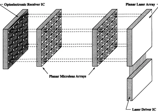
can exploit hardware parallelism, creating a multiplicity3 of optical links on a die using simple VLSI replication techniques. Figure 2-2 shows such a configuration for 40 optical channels. Jurgen successfully demonstrated 1024 such optical channels using planar microlens arrays [Jah90O].
In Figure 2-2, a separate laser array is used to transmit optical signals to an optoelectronic receiver chip. The microlens arrays are used to correct beam divergence for this free-space configuration. Alternatively, the detectors on the receiver chip can be pitch-matched to a fiber ribbon array carrying the optical signals. The fiber array is then be butted up against the receiver chip's surface, and then the whole assembly is sealed into a package. The fiber cable could then be separated at an inline optical fiber connector in case disassembly was required. Alternatively, the fiber could be mounted up against a transparent optical window in the chip's package.
Planar Microlens Arrays /
Figure 2-2: Parallel Optoelectronic Interconnect Links
The parallel optical link shown in Figure 2-2 uses separate transmitter and re-ceiver array chips rather than bidirectional chips. This hybrid approach is required
3
hundreds or even thousands of interconnects depending upon die size, and the area of overhead electronics required
for a technology such as Si because integrated photodiode detectors have a peak re-sponse to light with a wavelength around 850 nm.4 However, successful microlaser
arrays which emit light near 850 nm are typically made from GaAs-AlAs or GaInAs materials [LJ+89, JL+89, JML+89]. For each side of a bidirectional link, the re-ceiver electronics for incoming signals and the laser driver circuitry for the return direction can be integrated into one IC. The laser array chip is then mounted near the electronics chip. Next, the two chips are interconnected through wire-bonding or bump-bonding technologies.5 Obviously, this electrical interconnection degrades
overall link performance. If lasers with wavelengths near 850 nm could be reliably and cheaply integrated with Si circuitry, however, a bidirectional Si optoelectronic VLSI chip could, theoretically, be produced.
Not only does parallelism in optoelectronic links lower costs, especially for tech-nologies like Si, but it also provides a convenient medium for fault-tolerant, reliable interconnections through redundant spares and error detection and correction tech-niques which are readily implemented in VLSI electronics. Furthermore, in Si mono-lithic optoelectronic VLSI designs, where the available bandwidth is lower than in other, heterogeneous technologies, like GaAs, several slower, parallel Si optical links can replace a single ultra high-speed link, in order to reduce costs yet maintain all the other benefits of optics.
2.4 Attenuation Factors
For high frequencies (in and above the GHz range), electrical interconnect bandwidth is limited by the resistance, skin effect, and dielectric dispersion of wires [DKR+90]. The frequency-dependent dispersion of optical signals is much less than that of elec-trical signals over the range of distances used in interconnections because optics does
not rely upon conduction. Absorption, scattering and misdirected light comprise the
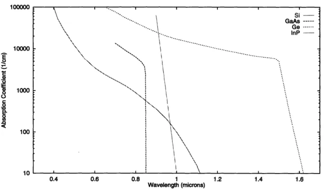
main loss factors in an integrated optical system. Figure 2-3 shows the attenuation
4The reason behind this phenomena is due to the intrinsic responsivity of Si, which is explained
in more depth in Chapter 3.
as a function of frequency for various types of optical and electrical transmission mediums [C090]. Transmission Loss 1 e+03 e+02 1 e+01 1 e+00 1e-01 e-02 e-03 1 1 1 e-04 1 10 Frequency (MHz) 100 1000
Figure 2-3: Attenuation of Optical and Electrical Interconnections
2.5 Fanin and Fanout Limitations
The fanin and fanout of optical signals is huge because optical signals require very little power and can cross without interference, unlike their electrical counterparts. In fact, in a 1mm2 area, an estimated 104 optical signals can coexist;6 104 parallel wires in such an area is impractical.
6This assumes a 2-D array (100 X 100) of 10,000 5-micron diameter beams each carrying a 1
Gb/s signal. -- ---8 um Cu Film -15 urn Cu Paste ---0.63 um Si Waveguide ---0.63 um Single-mode Fiber ...
0,85 LUM Single-fflode Fiber ...
E co 0 .J 1 -... .~ ... ... ... ... ... --- ·.--- ··-- ·-- -··--··--·- · ·· ··- ··- ··- ··- ··-···-···--·-:
In an actual implementation of an optoelectronic receiver system, a photodetector-receiver combination converts an optically modulated signal back to its electrical form. Typically, these components limit the bandwidth of the entire link. Therefore, in order to achieve high bandwidth, it is often necessary to integrate the photodetector and receiver on the same chip. Additionally, for monolithically integrated optoelectronic interconnects, the area of the photoreceptors and amplifiers may severely limit the interconnect density; therefore, it is vital to keep this area small.7
2.6 Impedance Mismatch Noise
Free-space optical interconnects do not require precise impedance matching. Fiber-optic links, however, require more careful impedance matching so that reflected Fiber-optical energy will not feed back into the source laser and degrade its performance [C090].
Electrical interconnects are limited by the fact that they must drive inherently
low-impedance transmission lines - typically around 50 Q. The low impedance drivers required for such a transmission line consume considerable chip area and power. Op-toelectronic devices can be made small, with relatively low impedances, and they will efficiently convert to and from the free-space optical impedance of 377 Q. In other words, an optoelectronic interconnect is a special type of optical isolator. It functions as an ideal transformer, isolating two separate voltages in circuits and performing well even down to DC frequencies [Mil90]. In this manner, it can handle arbitrarily long strings of "one" or "zero" in a non-return to zero (NRZ) digital system, though most systems require some means of coding to facilitate clock recovery on the receiver end.
As Knight [T. 89] pointed out, electrical interconnections tend to be one-to-one in nature to achieve high speeds and easy termination of transmission lines. High speed transmission lines can be broadcast to multiple points (multidrop line), however, termination of such lines to match impedances can be extremely difficult, especially
7
Keeping areas small also ensures detector and other parasitic capacitances are small which lowers required communication energy.
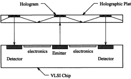
when signals go off-chip and parasitic package inductances as well as capacitances must be considered. Free-space or planar imaging techniques using microlens arrays or holograms [Jah90, Fel90] can be employed to broadcast an individual optical signal to many destinations with low interarrival skews due to matched transmission distances and the low noise properties of optical propagation. Moreover, free-space optical interconnects do not experience back-loading effects, and are, thus, limited only by the available power and detector area that must be covered. In fact, thousands of interconnections can be easily accommodated with a single lens [Mi190].
These combined facts encourage using optical interconnections to solve many prob-lems with high speed clock distribution. Figure 2-5 depicts a monolithic optical ap-proach to synchronous clock distribution in a digital system. In such a configuration, redundancy of emitters and receivers can increase reliability and reduce mechanical alignment problems. Another example of integrated optics comes from the work of Jahns [Jah90]. Figure 2-4 depicts an integrated optical imaging arrangement with 2-D microlens arrays.
I ight T irht
Input Output
artz
bstrate
reflective bottom surface
Figure 2-4: Integrated Optical Imaging System
2.7 Switching Noise
Another effect which can degrade the performance of electrical interconnect systems is noise caused by high-frequency switching transients. This noise voltage can be modeled as NLdi where N is the number of simultaneous switching elements, L is the effective inductance, and d dt is the slew rate of the driver. In order to minimize this
Hologram > r Holographic Plate
electronics Emitter electronics
Detector Detector
VLSI Chip
Figure 2-5: Synchronous Optical Clock Distribution
effect, the driver can be slowed, the number of simultaneous switching elements can be minimized, static and dynamic ground loops - which arise out of the difficulty in maintaining a constant ground potential throughout a system - can be broken, or decoupling capacitors can be used. Slowing the output drivers degrades system performance considerably; reducing the number of simultaneous switching elements requires special partitioning and system designs; breaking ground loops requires spe-cial circuit isolation techniques; using decoupling capacitors may consume consider-able area. In typical low-noise electrical systems, the last three recommendations are usually employed.
2.8
Crosstalk Noise
Electrical signals are also degraded by interference due to stray capacitances and mutual inductances that exist between nearby transmission lines. Crosstalk noise only becomes worse for higher frequencies and denser circuits [Rub90a]. Optical systems, however, only experience small evanescent wave coupling between adjacent waveguides, neglecting scattering due to surface roughness and waveguide interfaces.
2.9 EMI Immunity
Because optics does not rely upon transduction except at the electronic interfaces, it is immune to EMP susceptibility, crosstalk, frequency dependent loss, and impedance mismatches, unlike electronics, which experiences all of the above effects. These factors lead to the high reliability of optical systems.8
2.10 Mutability of Connections
One of the major advantages of optics over electronics - the ability to make and break connections easily - stems from the fact that no physical contact is required to make optical interconnections, unlike electronics.9 Electronic interconnects, on
the other hand, require mechanical contacts and bonding / debonding. Bonding 105 connections is unwieldy for electronics, and is no concern for optics, however, mechanical alignment of the optical beams may be difficult.
Some of the direct consequences of the mutability of optical interconnections in-clude the following [Cau90]:
* connections between removable objects * connections between remote objects * large number of connections
* "smart" or selective connections: with the merger of optics and complex elec-tronic logic, connections can adapt to meet system signal-to-noise requirements, to take advantage of redundant hardware for fault-tolerance, to monitor and output vital link statistics (such as Bit Error Rate, BER, and available band-width), and to take advantage of electronic error detection and correction (EDC)
circuitry.10
8Laser lifetimes have improved, and spatial modulators provide an alternative solution to the
laser isolation problem.
9Even capacitively coupled techniques require precise control of inter-plate separation distances. 1°Optics is great for regular patterns like a "perfect shuffle", but electronics is much better at
2.11 Reliability Concerns
The reliability of a large system made up of many identical components can be ap-proximated by the reliability of one of the components divided by the number of such components in the system. The approximation holds true for random failures (which as a result of being a Poisson process, have exponential first-order interarrival times), not those due to component wear out (which have a log-normal distribution) [Ols93].
For example, a system composed of 1000 lasers each having a random failure time of 105 hours will have a mean time between failure (MTBF) of about 100 hours. Wear out failures will only increase this rate.
Many aspects of electrical connections can lead to system reliability problems. Electrical connectors, being mechanical in nature, can make lossy connections, or simply wear out from excessive make-break cycles. Moreover, VLSI systems can experience mechanical bonding problems due to poor alignment or thermal expansions of dissimilar materials, and electromigrationll or component failure can also cause system failure. All these effects lower overall system reliability.
Optical interconnections also suffer from alignment problems, but none of the other mechanical limitations of electrical connections. The lifetime of monolithic lasers used in optical interconnections follows the traditional "bathtub" curve, where in the early stages of use, the rate of laser attrition due to component failures is
high, then the rate decreases for quite some time, and finally, the laser extinction
rate increases again due to wear out [Ols93]. The wear out of a semiconductor laser results in an increased threshold current,12 making driver feedback circuits necessary
in order to adjust the laser bias current to achieve a constant BER over time (before final failure).
Finally, electrically wiring two electronic gates in parallel to improve system yield and reliability will not work. If the gates were connected optically, however, then the
irregular connections: some hybrid combination may be needed to produce low area and efficient logic utilization.
llCu deposited by chemical vapor deposition (CVD) can be used to increase resistance to
electro-migration and increase conductivity over traditional Al wiring [Shr90O, DKR+90].
1 2
setup would work. Fault-tolerance through optical interconnections and redundant electronics is easy to implement because of the unidirectional nature of free-space optical interconnections versus the bidirectional character of electrical wires [Hua91].
2.12 Communication Energy
Electrical interconnections can be modeled in two distinct manners [Kim91]: for short distances, a lumped RC model will suffice; for longer distances, a distributed transmission line model should be used. For the lumped RC case, the entire line must be charged to a final voltage and then discharged. Thus, the required energy is
Ee= CtV2 , (2.1)
where Ct is the total line capacitance, including output driver and input receiver capacitances. For inter-chip communication, the input and output bonding pad ca-pacitances would also be included. In the case of a distributed transmission line, only the length of line corresponding to the pulse width must be charged. The required energy follows the same equation as for the RC case, except that Ee is independent of interconnect length.l3 The length of interest (pulse width) is
c
Lpw, = pw, (2.2)
where c is is speed of light, rp, is the pulse width of the signal, and cE is the relative dielectric permittivity of the material ( .t) which is 3.9 for SiO2. Moreover, all high speed transmission lines must be terminated. The additional power that is dissipated due to a series-terminated line in the round-trip time of the line can be expressed as
Pt = 2 (2.3)
l3However, the resistive losses in a long line may require the use of repeater amplifiers, hence, increased required energy.
where R, the termination resistance, is matched to the characteristic impedance, Z,
of the line. Figure 2-6 shows such a series-terminated transmission line.
ram.~ ,~T-t 0in
+
)
Vs
Transmitter Receiver
Figure 2-6: Series-Terminated Electrical Transmission Line
For an optical interconnect link, the total capacitance that must be driven is the
photoreceiver plus amplifier input capacitances. The energy required to drive the laser can be expressed as
El = 2 x 3TPL, (2.4)
where the laser driver is assumed to be 50 percent effective in delivering power to the laser, PL is the average laser output power required, and T is the rise time of the
signal which is assumed to equal the fall time; the total pulse time is estimated at
3T. An expression for r comes from the characteristic capacitance relation:
r = Ct
,
(2.5)
IPD
where Ct is the total driving point capacitance as mentioned above, V is the
volt-age swing needed at the receiver input, and IPD is the photodetector current. The photocurrent follows the relation:
q(PL -Pth)71
IPD -- (2.6)
where q is the electron charge, Pth is the required power to bias the laser at threshold, r7 is the overall link efficiency (which is the product of the external laser quantum
efficiency), h is Planck's constant, and v is the operating frequency. The above ex-pressions can be substituted into the original power expression to obtain the required power for the optical interconnect:
El = 6CV [rhPL ] (2.7)
Figure 2-7 depicts a typical free-space optical communications link, where o, is defined to be the impedance of free space, 377 Q. The transmission end consists of a laser which is driven by a modulated voltage source (a simple switch is the modulator here); the receiver end is comprised of a photodiode and amplifier. The amplifier operates in the transimpedance mode with an open loop gain of -A. More details will be provided on this configuration in later chapters.
Rf Vs Laser
-v---__
710 'Lens Vo Transmitter ReceiverFigure 2-7: Free-Space Optical Communication Link
The high quantum efficiency of today's semiconductor lasers (around 80 percent) translates into about 1mW of optical power produced from mA of electrical current. Photodiodes with over 80 percent quantum efficiency are also manufacturable. Elec-trical drivers, on the other hand, require about 10-20mA switching current which is an order of magnitude higher than their optical counterparts [CO90].
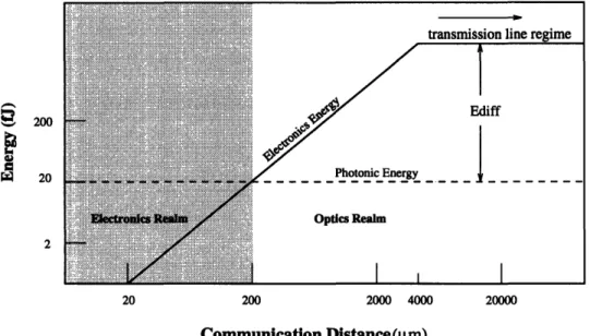
Communication energy is actually only less for optics than for electronics when the distances for communication are greater than some critical length. Figure 2-8 based on Huang and Miller [Hua91, Mil90] depicts the critical communication distance where optics is more energy efficient than electronics for the same BER, ignoring cost
concerns. The critical distance of 200 ,um shown would be closer to about 200 cm if today's costs are taken into account, however, with optics prices dropping (especially due to integration) and optical efficiencies increasing rapidly, this critical dimension will continue to decrease [Mil90].
... ...
transmission line regime
200 @ 20 . . . .. Photoni_ic Energy_ Optics Realm 2
-~~~~~~~~~~~~~~~~~~~~~~~~~~~
20 200 2000 4000 20000 Communication Distance((gm)Figure 2-8: Communication Energy Versus Distance
Notice that for communication distances beyond 4 cm (4000 pm), the electron-ics energy curve remains constant. This phenomenon occurs because the electrical transmission medium is transformed into a transmission line, which when properly terminated, requires constant energy, independent of length.14
Figure 2-8 assumes that the communication channel rate is 1Gb/s, NRZ. An electrical wire can be modeled as a transmission line when the length of the wire is
shorter than one-fourth of the signal's wavelength. The signal's wavelength can be
calculated as follows:
sg -= fsipr (2.8)
where vp,op is the characteristic velocity of the signal propagating down the wire which
14However, extremely long transmission lines require repeater amplifiers to compensate for resistive
is assumed to be around 15 cm/ns (0.5 ft/ns), and fs,ig is the frequency of the signal.l5 For a 1Gb/s NRZ signal,
15cm/ns
1Gb/s -
Ins
= 15cm. (2.9)Therefore, if the length of the electrical interconnect is longer than about 4 cm, it can be modeled as a transmission line. The energy difference, Ediff, should also be evaluated in order to determine if the additional cost of optics over electronics is justified.
Chapter 3
Si Optical Sensors
One basic rule that most VLSI designers have in the back of their mind is:
Use silicon... except when you can't.
3.1
Overview
This chapter begins with a description of photosensor operation including important device parameters and their inter-relationships. Next, the discussion turns to various
designs of monolithic Si photodetectors which are compatible with standard CMOS processes. Mathematical expressions (derived in Appendix A) governing important device parameters are used to analyze possible design tradeoffs to optimize device performances under various constraints. These tradeoffs are incorporated into the photogen CAD program of Chapter 4.
Silicon comprises over 70 percent of the earth's crust. The material properties of silicon include such desirable traits as visible light sensitivity, room-temperature operation, and relative ease of manufacturing. These facts make it an ideal material for many photodetector applications. In the 200 to 1100 nm regime - which includes the visible spectrum - silicon is most sensitive, making it the most popular choice for optical sensor material. Also, many vendors offer competitive silicon detector solutions in high-speed packaging styles [Ham90, Sie90O, Tex90O, Adv90, Mot88, Opt90].
3.2 Photosensor Types
The three main categories of photosensors are depicted top-to-bottom in Figure 3-1. The various photodiode and phototransistor types all operate on the same basic principle. Because of carrier concentration gradients at a P-N semiconductor junction, electrons in the N-side diffuse across the boundary to the P-side, and holes diffuse in the opposite direction from the P-side to the N-side. The diffusion process creates a counterbalancing electric field in equilibrium which appears across the junction and results in a built-in device voltage.' A small region around the junction is thus depleted of mobile carriers, and hence, is termed the depletion region.
RX+iPorN o
Photoconductor
Pj| N ho ASPI I N[o So N+ P IP+ O
PIN Photodiode Avalanche Photodiode
Vgs
Phototransistor (BJT) Phototransistor (MOSFET)
Figure 3-1: Photodetector Types
A photon from an incident light beam creates an electron-hole pair in the material
only if its energy2 is greater than or equal to the bandgap energy, EG, of the material.
EG is 1.12ev for silicon; the wavelength corresponding to the bandgap energy of the
1This voltage may be nullified at the device terminals by proper choice of metal contacts which create metal-silicon diodes
2Ep = hv where h is Planck's constant and v is the frequency of light
Photodiode [tIp (1) Ip . I I . . . . I ak
material is termed the critical wavelength,3 A. This critical wavelength represents
the longest optical wavelength which will generate electron-hole pairs in the material. Electron-hole pairs produced within a diffusion length of the depletion region are eventually separated by the electric field and the carriers are swept across the junction to produce a current flow in an external circuit. Carriers outside this region recombine
and thus, do not contribute to the photocurrent.
3.2.1 Photoconductor
The photoconductor is the simplest optical sensor that can be designed. It consists of a slab of semiconductor material which is typically doped N-type or P-type to tightly
control its characteristics. When photons with energies above the bandgap of the
material are absorbed in the material, electron-hole pairs are produced4 which increase
the material's conductivity. If an external voltage is applied across the device, the measured current will be proportional to the light intensity. In a real device, there are many processes that can degrade performance. Carrier trapping, recombination, and thermal generation of carriers can cause non-linearities [LHA+93]. Also, absorption may occur for photon energies less than the band gap because of lattice defects or
impurities.
3.2.2 Photodiode
Figure 3-2 depicts an equivalent circuit model for a photodiode [Ham90O]. IL represents the photo-generated current which is proportional to the incident light intensity, ID is
the diode junction current, Cj is the junction capacitance, Rsh is the shunt resistance,
R, is the series resistance, Ih is the shunt current, VD is the diode voltage, and I,o is
the output current.
Given the aforementioned circuit model, and the Shockley ideal diode equation,
3
A = = 1.1pm for Si
4which is the same as an electron being promoted from the valence band to the conduction band,
\ I 1'P
-
--+ i tID Ishtl kL CJ Rsh Vo Io + i - -AXt-o RsFigure 3-2: General Photodiode Circuit Model
one can solve for the output current, which is
IO = IL - ID - Ish
Upon making the Schottky diode equation substitution, this becomes:
Io
=
IL-
Is(e
k-1)-Ih
,
(3.1)where I is the diode saturation current. The open circuit output voltage, Vc is also easily to derive from the Schottky diode equation and the fact that ID = IL - Ish:
ID =
Is (ekT
- 1)n (ID + 1 = qVD
kT
Vc
kT
(IL - Ish + 1) (3.2)Equation 3.2 clearly illustrates the logarithmic dependence of the open-circuit output voltage on light intensity when IL is large compared to Isha Voc also varies considerably with temperature, making this photovoltaic diode mode difficult to use for light intensity measurements.
Finally, the short-circuit output current, I,, can be calculated:
1l b b | b * A
~8C
=
hR. + Rsh)
I
= (R +R )IL
-
R
)
Is
(e1)
(3.3)
In Equation 3.3, the diode nonlinearities arise from the exponential in the second term. If the value of Rs is made very small (under 1 Q) and the value of Rh very large (tens of MQ or higher), then I will be very close to IL. Typically, a photodiode is operated with a very low load resistance, or even a reverse-bias voltage applied (V, < 0) to increase response linearity and speed. This last, reversed-biased condition is termed the photoconductive or photocurrent5 mode of a diode.
Figure 3-3 shows the reduced circuit model for a photodiode used in the photocur-rent mode, where the diode has a reverse-bias voltage applied. Rh is the parallel shunt resistance, Cj is the parallel junction capacitance, and Rs is the series resistance of the device. Notice that the direction of photo-induced current flow is in the opposite direction of conventional current. A photodiode can also be used in the photovoltaic mode, where no reverse-bias voltage is applied, and a photo-generated voltage ap-pears from anode to cathode when incident light strikes the diode junction. A solar cell is an example of a photodiode operated in this mode. The photocurrent mode offers performance advantages over the photovoltaic mode in terms of its linearity, response speed, capacitance, stability, and temperature coefficient; therefore, unless otherwise stated, all photodiode designs to follow are assumed to operate in the pho-tocurrent mode. For photodiodes operating in the phopho-tocurrent mode, typical range of values for Rs is 10 to 100 Q, Rsh is 109 to 1010 Q, and C is highly dependent upon processing and area [Mil86].
The PIN photodiode enhances the simple PN photodiode's characteristics by pro-ducing the same amount of current for a lower device capacitance. As a consequence,
5
This name is a misnomer because the photodiode is always a current source, with or without an
I; -L 1CJ X Rsh Vo
Rs Figure 3-3: Photocurrent-mode, Photodiode Model
it offers a faster response as well. An additional intrinsic, (high resistance) region, I, sandwiched between the P and N regions. This intrinsic region is depleted in normal operation along with the P and N regions, providing a much larger collection region for electron-hole pairs than a simple PN diode, and greater resistance to breakdown voltage and leakage. Moreover, the intrinsic region thickness can be tailored to opti-mize responsivity and response time. Typical PIN photodiodes have been fabricated to have quantum efficiencies at or near 100 percent [Ham90, Adv90]. The capaci-tance of a PIN photodiode is lowered significantly because the effective "plates" of the capacitor have been spread apart by the length of the I region.
The avalanche photodiode requires a huge6 reverse-bias voltage to create the high
electric field required for avalanche multiplication. Optically generated carriers are swept into this high field region and accelerated. There, electrons and holes impact with other atoms and cause secondary electrons and holes to be produced, and these new carriers cause yet more carriers to be produced, and so on, effectively multiplying the number of carriers. The gain produced is on the order of 50 to 500 without a cost in speed, so this device is great for sensing low light levels. However, the large bias voltage required, the noise generated by the random carrier multiplication process,7 and the temperature compensation needed for stability further complicate their use in monolithic integrated optoelectronic circuits today.
As depicted in Figure 3-4, MSM (metal-semiconductor-metal) diodes consist of closely-spaced interdigitated metal electrodes atop a semiconductor material.
Volt-6
150V to 300V is typical
7
the receiver sensitivity can be improved by using a APD, but only as long as the multiplication noise is less than the noise of the amplifier
ages of opposite polarity are applied to adjacent electrodes to produce strong electric fields between the electrodes. These high electric fields sweep optically-generated car-riers out of the exposed, underlying semiconductor material, allowing the carcar-riers to be collected at the electrodes. The most common type of MSM photodetectors used today in optoelectronic applications are of the Schottky barrier variety, which have rectifying contact(s) from the metal to the semiconductor layer. The use of rectifying contacts guarantees that the dark current will be dominated by the thermal injection of electron-hole pairs in the semiconductor region where they are generated [JP86]. MSM photodetectors have advantages of planarity, simplicity, and compatibility with FET processing technology, and are used in many GaAs-based receivers. However, the Schottky barrier potentials on simple structures are often low, and in order to limit the dark current in such devices, special contact metals, extra semiconductor layers, and processing steps are often required to boost the Schottky barrier levels [SS90]. The MSM detector design is not compatible with an unmodified Si CMOS process, and thus was not considered an effective Si detector for this thesis investigation.
+
+ [
[
Figure 3-4: Schottky MSM Photodiode
3.2.3 Phototransistor
A bipolar phototransistor can be modeled as a bipolar transistor with a photocurrent injected between the collector and base. The transistor amplifies the photocurrent by the beta of the device, producing a much greater current at the emitter or collector.
However, the performance penalty is speed - the photocurrent must charge up the
base-emitter capacitance which increases rise and fall times drastically. Moreover,
beta variation translates into uncertainty in sensitivity.
A light-sensitive MOSFET can be created by fabricating an N-channel transistor in a P-well process, applying a positive gate-to-source voltage to ensure the transistor is not in the cutoff region, and leaving the well connection floating [KDJS87]. MOSFETs can be rendered light-insensitive by tying their P-well (for an nFET) to ground, or N-well (for a pFET) to VDD, or by shielding the device with a metal layer over the
device.8
In the linear regime, the device's current response has been shown [KDJS87] to vary logarithmically with light power according to the following relation:
IDS
= /3 {[Vs-VthO-K1
(V2F- VTln(1
+RPPopt/Io)-
24F)] VDS-}
(3.4)
where: W LnOEox = W n o (3.5) L 'ox VT = k, (3.6) q F = kT n NP-well [ (3.7) q ni K1 = 2qNp-well -- (3.8)
Io is the junction reverse-bias saturation current, Popt is the light power in /W, and R is the responsivity which is defined in Section 3.3. Vtho is the nonilluminated threshold voltage, and Np-_,, is the donor concentration per cm3 in the P-well.
At the P-well and substrate P-N junction, optically generated holes are swept into the P-well region, which causes electrons to flow across the source and P-well
8
Shielding all non-photonic devices near the area where light impinges on the chip is a good idea
in order to lower minority carrier injection into the substrate - current which can cause latchup in
N-P junction in order to regain equilibrium. Most injected electrons flow into the channel region if the source area is small, increasing the drain current; otherwise, many electrons get pulled down across the P-well and substrate P-N junction, creating a parasitic 9 vertical bipolar phototransistor mode of operation.
If the MOSFET's source area is too large, this parasitic bipolar device can degrade optical response of the device, and, for high enough light intensities, may lead to
CMOS latchup. Hence, the photo-MOSFET has an inherent size constraint which
may limit its application usefulness, especially in the niches of strip detectors and alignment-tolerant systems. Also, for large VD values, impact ionization (avalanche multiplication) has been shown to occur in the pinch-off region of the channel near the drain. This effect dominates over photo-induced currents; therefore, the device should be operated with low VDS voltages to obtain optimal photo responsivity. Because of
these limitations, the optical MOSFET will not be considered as candidate detector
for the CMOS photodetector CAD tool in Chapter 4.
3.3 Important Photodiode Parameters
This section describes parameters which are vital for proper design or selection of photodiodes which operate in the photoconductive mode. For mathematical deriva-tions of the parameters discussed below, please refer to Appendix A. A useful table containing important device design parameters may be found in Appendix B.
3.3.1
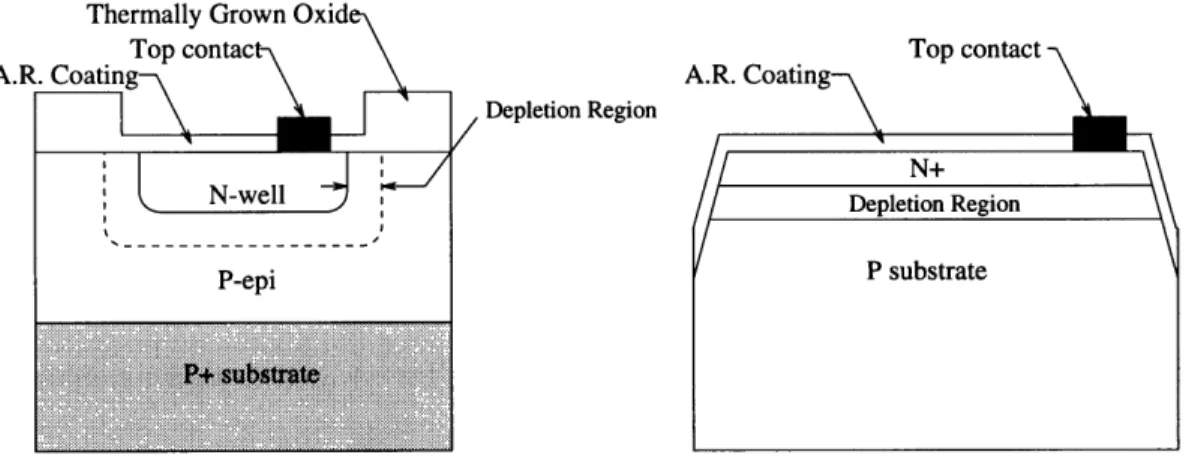
Active Area
Two different photodetector diffusion types [LHA+93] are shown in Figure 3-5. For the mesa type, the PN junction emerges on the sides of the device, so it is difficult to passivate this junction area with oxide. Therefore, it is often exposed and vulnerable
to contamination and atmospheric degradation. Also, the top area of the device,
9
This parasitic N+/P-well/N-sub device can be used by itself as a CMOS process-compatible
bipolar phototransistor as long as care is taken to limit minority carrier injection into the substrate and to isolate these devices far from CMOS circuits.
which is unshielded by any protective or routing metal layers, is defined as the device active area. In a planar type detector, on the other hand, the PN junction emerges at the surface of the device, around its perimeter, where it usually is passivated with an oxide layer. This makes it much more reliable. For an applied reverse-bias voltage, a depletion region forms across the diode's PN junction including the surface junction. This surface depletion region, if unshielded, effectively extends the active device area beyond the area defined by the lithographic masks. If the geometry is carefully planned, this surface depletion region can be used to maximize device responsivity through the use of the vertical PN junction feature, at the expense of photodetector response uniformity.'0 The photogen tool in Chapter 4 has an option to generate photodetectors which rely upon this principle.
Depletion Region
1. Planar diffused pn junction photodiode 2. Mesa diffused pn junction photodiode
Figure 3-5: Photodiode Junction Diffusion Structures
3.3.2 Breakdown Voltage (reverse bias)
When the internal electric field of a reverse-biased photodiode exceeds about 3 x 10⁵ V/cm,"l a high-field effect known as impact ionization is initiated. This is the same effect which causes carrier multiplication in an avalanche photodiode. The
10It does this by absorbing photons along the tub edge, which extends deeper into the substrate than any other diffusion feature.
11This number depends upon the doping levels, and can range from 2 x 10⁵ V/cm to 8 x 10⁵
V/cm for Si.
A.F
_--external reverse-bias voltage which must be applied to the device to support such a high internal electric field is termed the breakdown voltage of the device. For a simple abrupt junction PN diode, the maximum electric field - which occurs at the junction edge - can be expressed as
IqI
i(
=
NA+ND) (Vi +Vev).
(3.9)
Assuming that Vrev > Vbi and solving for V,,r, we get:
Vb = Vrev = (
2x
)[
NA + N]
(3.10)
Assuming the diode's built-in voltage is 0.6V, and the ionized donor concentration is 1015, the applied reverse voltage, Vrev must be around 584V to support a maximum electric field of 3 x 10⁵ V/cm.
For a PIN diode, the breakdown voltage, Vbr, can be expressed simply as
Vbr = IemaI W - Vbi , (3.11) where W is the width of the intrinsic (depletion) region.
To support a maximum electric field intensity of 3 x 10⁵ V/cm, the PIN diode
must have a reverse voltage of about 300V applied.
Because voltages in typical integrated circuits are nowhere near this high break-down voltage, the avalanche mode of a typical photodiode cannot be utilized by monolithic photodiodes in optoelectronic circuits. This parameter is often ignored in monolithic photodiode designs, except in the case of providing electrostatic discharge (ESD) protection for small devices.
3.3.3
Capacitance
The junction (depletion-layer) capacitance of a silicon PN diode is simply the
capac-itance of a parallel plate capacitor with plate separation W and stored charge equal
charge layer). This implies:
EsiA
CJ = (3.12)
cw
where A is the cross-sectional area of the diode, W is the depletion region width, and si is the permittivity of silicon. The depletion widths of an abrupt-junction PN diode and a linear-graded PN diode can be expressed as
Wa = ](2si) NA + ND (Vi + V, 2V) , (3.13)
Wgj
=12si (i + Ve - 2V) ,
(3.14)
qa where: Vbi = ln( NAND , (3.15)kT
Vt = (3.16) qND is the ionized donor concentration in the N-material, NA is the ionized acceptor concentration in the P-material, Vbi is the built-in voltage (usually around 0.6V), Vt is
the thermal voltage, (0.026V for room temperature [300K]), a is the doping grading coefficient, Vrev is the applied reverse-bias voltage, and ni is the intrinsic carrier concentration of silicon.
If NA > ND, as is the case in a one-sided abrupt junction, Equation 3.13 reduces
to
Waj
=
qND (3.17)The capacitance per-unit-area expression for a reverse-biased abrupt-junction PN diode is
Co -
qpsiNND
(3.18)
J
2(NA + ND)(Vb + Vr - 2Vt)
For an abrupt, one-sided junction, assuming NA > ND, Equation 3.18 reduces to
qesiND
aj = 2(Vbi + Vrev - 2Vt) (3.19)
For typical (small) optoelectronic photodetector device sizes and technologies, the
junction capacitance is also usually small. The diode's RC time constant1 2 limits its
speed of response. Since R, and Rh can be ignored most of the time, the detector circuit-limited frequency response can be expressed as
V~.(f)
KV~in.~
R(~
)
(3.20)
~R
Iph(f) 1
+
j27rfRL Cj
However, for PIN structures with wide depletion regions, the diode's bandwidth is usually limited by the transit time of photo-generated carriers across the depletion region. Moreover, when the diode is actually connected to a circuit, its total ca-pacitance adds to the front-end (receiver) caca-pacitance which can significantly impact receiver sensitivity.
3.3.4
Crosstalk (for arrays)
Crosstalk between adjacent detector array elements is defined as the ratio of the pho-tocurrent generated in a dark detector to the phopho-tocurrent generated in an adjacent,
60-80 percent illuminated detector [Ham90O]. The intensity of illumination is adjusted to achieve a specified output current in the illuminated detector. This parameter is
extremely important for arrays because strong crosstalk can significantly degrade the
S/N ratio on a particular channel.
12rRC RL Ct where RL is the load resistance of the circuit to which the diode is connected, and Ct is the total capacitance of the diode.