Doppler Channel Emulation of High-Bandwidth
Signals
by
Joseph William Colosimo
B.S., Massachusetts Institute of Technology (2012)
Submitted to the Department of Electrical Engineering and Computer
Science
in partial fulfillment of the requirements for the degree of
Master of Engineering
in Electrical Engineering and Computer Science
at the
MASSACHUSETTS INSTITUTE OF TECHNOLOGY
June 2013
©Massachusetts Institute of Technology, 2013. All rights reserved.
Author . . . .
Department of Electrical Engineering and Computer Science
Jun 1, 2013
Certified by . . . .
Aradhana Narula-Tam
Assistant Group Leader; MIT Lincoln Laboratory
VI-A Company Thesis Supervisor
Certified by . . . .
Muriel Medard
Professor of Electrical Engineering and Computer Science
MIT Thesis Supervisor
Accepted by . . . .
Dennis M. Freeman
Chairman, Masters of Engineering Thesis Committee
Doppler Channel Emulation of High-Bandwidth Signals
by
Joseph William Colosimo
Submitted to the Department of Electrical Engineering and Computer Science on Jun 1, 2013, in partial fulfillment of the
requirements for the degree of Master of Engineering
in Electrical Engineering and Computer Science
Abstract
The Airborne Networks Group at MIT Lincoln Laboratory has funded the construc-tion of a channel emulator capable of applying, in real-time, environmental models to communications equipment in order to test the robustness of new wireless communica-tions algorithms in development. Specific design goals for the new emulator included support for higher bandwidth capabilities than commercial channel emulators and the creation of a flexible framework for future implementation of more complex chan-nel models. Following construction of the emulator’s framework, a module capable of applying Doppler shifting to the input signal was created and tested using DVB-S2 satellite modems. Testing not only verified the functionality of the emulator but also showed that DVB-S2 modems are unequipped to handle the continuous spectral frequency shifts due to the Doppler effect. The emulator framework has considerable room for growth, both in terms of implementing new channel transformation models as well as the re-implementation of the emulator on custom hardware for emulation of channels with wider bandwidths, more complex noise sources, or platform-dependent spatial blockage effects.
Thesis Supervisor: Aradhana Narula-Tam
Title: Assistant Group Leader; MIT Lincoln Laboratory Thesis Supervisor: Muriel Medard
Acknowledgments
MIT’s VI-A program1 made this thesis possible. Through VI-A, MIT Lincoln
Labo-ratory gave me access to a wealth of amazing people and resources. My sincere thanks to Kathy Sullivan for her work to keep VI-A running smoothly.
Group 65 leader Matt Kercher was my supervisor, mentor, and friend. He was also always happy to provide whatever resources he could to aide in the completion of this project that he had originally envisioned. His guidance was indispensable.
I’m enormously thankful for Chayil Timmerman’s help. For nearly a year, he mentored me in the art of digital design in timing-constrained systems; I learned much. He even let me steal his lab equipment for extended periods of time.
I would also like to thank Aradhana Narula-Tam, assistant group leader, for her advice, as well as group administrator Evelyn Bennett, who made sure I always had the resources I needed. My thanks to Larry Bressler and Ed Kuczynski as well.
Professor Muriel Medard graciously agreed to become my faculty thesis advisor very late in the game. My department advisor, Jeff Shapiro, was always kind to his advisees throughout our years at MIT. I also had the great fortune of being able to spend some time with Professor Jim Roberge, the VI-A liaison to Lincoln Lab.
The initial seeds of interest in digital design were planted by Roberto Acosta at BAE Systems and Gim Hom at MIT. In that way, they have played a major role in where I have chosen to direct my interests and time.
My friends have been a continuing source of both healthy distraction and motiva-tion. 3pm coffee breaks with Karen Sittig often got me through frustrating days. I am deeply thankful to Qiaodan Jin Stone for her continued support.
Finally, I am eternally indebted to my family, especially my parents, who made great sacrifices to give me opportunities they never had. I am truly thankful each day for their support and love. I can only hope that I have done their hard work a modicum of justice.
1
Contents
1 Introduction 11
1.1 Comparison to Simulation . . . 12
1.2 Constructing a Channel Emulator . . . 13
1.2.1 Hardware Decisions . . . 14
1.3 Notation . . . 15
2 Understanding the Doppler Effect 17 2.1 Shifting a Sine Wave . . . 17
2.2 Shifting a Spectrum . . . 19
2.3 Intelligently Representing a Spectrum Shift . . . 20
2.4 Determining the Need for the Corrective Shift . . . 21
2.5 Defining vr in the Real World . . . 22
3 Signal Processing Architecture 24 3.1 Analog Pre-filtering . . . 25
3.2 ADC . . . 25
3.3 Downconversion . . . 26
3.4 Anti-aliasing Filter . . . 29
3.4.1 Data Capture and Buffering . . . 31
3.4.2 Tap Folding . . . 32
3.4.3 Multiplication . . . 33
3.4.4 Post-Multiplication Adder Tree . . . 33
3.6 Variable Mixer . . . 34
3.6.1 DDS Background Theory . . . 36
3.6.2 Implementing a DDS . . . 38
3.6.3 Mixer Architecture . . . 39
3.6.4 Parallel Lookup Tables . . . 39
3.6.5 Making the Mixer Variable . . . 40
3.7 DAC . . . 40
3.8 Analog Mixer . . . 41
3.9 Numeric Precision . . . 41
4 Implementation of the Channel Emulator 43 4.1 Hardware Considerations . . . 43
4.1.1 FPGA Evaluation Board . . . 44
4.1.2 Analog Interface . . . 45
4.2 Digital Hardware Architecture . . . 46
4.2.1 Clocking . . . 46 4.2.2 Picoblaze Microprocessor . . . 47 4.2.3 SPI Controller . . . 47 4.2.4 DAC Controller . . . 49 4.2.5 ADC Controller . . . 50 4.2.6 FIFO Dumper . . . 50 4.3 Configuring FMC110 Hardware . . . 51
4.3.1 Channel Emulator Configuration Interface . . . 52
4.3.2 Configuring FMC110’s CPLD and Clock Generator . . . 52
4.3.3 Configuring DAC0 . . . 52
4.3.4 Configuring ADC0 . . . 53
4.4 Configuring the Signal Processing Chain . . . 54
4.5 Applying Doppler Shifting . . . 54
5 dopgen Software Package 56 5.1 System Architecture . . . 56
5.1.1 Injectors . . . 58
5.1.2 Processor . . . 59
5.1.3 Coordinate Systems . . . 60
5.1.4 Serial Interface . . . 62
5.1.5 Logger . . . 62
5.2 Using Data from Pre-Recorded Scenario . . . 63
5.2.1 The EEL Pseudo-Standard . . . 63
5.2.2 CSV File Format . . . 64
5.3 Injecting Data from Flight Simulators . . . 64
6 Evaluating the Emulator’s Performance Capabilities 66 6.1 Bandwidth Limit Evaluation using a Newtec AZ-410 Modem . . . 67
6.2 Testing with High-Bandwidth Modem . . . 69
7 Testing Doppler Shifting Capabilities 78 7.1 Notes about Modem Data Capture . . . 79
7.2 Constant Airspeed Fly-By . . . 79
7.3 Flight Simulator Testing . . . 80
7.4 Flight Simulator Merged Path Playback . . . 81
8 Concluding Remarks 86 8.1 Looking Forward . . . 86
A cci – Channel Emulator Configuration Interface 88 A.1 Comments . . . 88
A.2 Inline Assembly . . . 88
A.3 Macro Reference . . . 89
A.3.1 fmcw DEV XX YY — SPI Write to FMC110 . . . 89
A.3.2 fmcr DEV XX — SPI Read from FMC110 . . . 89
A.3.3 fmcv DEV XX YY — SPI Write and Verify from FMC110 . . . . 90
A.3.4 ccfg DD AA — FPGA Module Configuration . . . 91
A.3.6 out REG, PORT — Shortcut for output . . . 91
A.3.7 in PORT — Read from port . . . 91
A.3.8 sndstr "STRING" — Sends a string over UART . . . 92
A.3.9 newline — Sends a newline over UART . . . 92
A.4 Producing Assembly Code . . . 92
A.5 Live Injection via Serial . . . 92
A.5.1 Additional Options . . . 93
A.5.2 CPU Prompt Architecture . . . 93
B VHDL Preprocessor System 95 B.1 Fooling GCC . . . 95
List of Figures
1-1 Channel emulation in a nutshell . . . 11
2-1 Doppler shifting example . . . 18
2-2 Doppler shift of a spectrum . . . 20
3-1 Signal chain overview . . . 25
3-2 Test input spectrum . . . 27
3-3 Output of DDC stage . . . 28
3-4 AA FIR filter shape . . . 29
3-5 AA FIR filter frequency response . . . 30
3-6 Output of AA FIR stage . . . 30
3-7 Architecture of the digital anti-aliasing filter . . . 31
3-8 Filter Buffer System . . . 31
3-9 Architecture of the post-multiplication adder tree . . . 33
3-10 Output of mixer stage . . . 35
3-11 Example of DDS output with varying phase ramps . . . 36
3-12 Mixer Architecture . . . 39
3-13 Revised variable mixer architecture . . . 41
4-1 FMC110 architecture . . . 46
4-2 Digital hardware architecture . . . 47
4-3 FMC110 SPI packet structure . . . 48
4-4 FMC110 DAC controller architecture . . . 49
5-1 dopgen Software architecture . . . 57
6-1 Channel emulator test setup . . . 68
6-2 EVM as a function of fc . . . 69
6-3 fc=1180 MHz input waveform from AZ-410 . . . 70
6-4 fc=1185 MHz input waveform from AZ-410 . . . 70
6-5 fc=1190 MHz input waveform from AZ-410 . . . 71
6-6 fc=1200 MHz input waveform from AZ-410 . . . 71
6-7 fc=1208 MHz input waveform from AZ-410 . . . 72
6-8 fc=1250 MHz input waveform from AZ-410 . . . 72
6-9 fc=1292 MHz input waveform from AZ-410 . . . 73
6-10 fc=1300 MHz input waveform from AZ-410 . . . 73
6-11 fc=1310 MHz input waveform from AZ-410 . . . 74
6-12 fc=1315 MHz input waveform from AZ-410 . . . 74
6-13 25 MSPS input waveform from high-bandwidth modem . . . 75
6-14 74 MSPS input waveform from high-bandwidth modem . . . 76
6-15 90 MSPS input waveform from high-bandwidth modem . . . 76
6-16 91 MSPS input waveform from high-bandwidth modem . . . 77
7-1 Aircraft fly-by test path . . . 79
7-2 Distant fly-by frequency shift . . . 80
7-3 Close fly-by frequency shift . . . 81
7-4 Live system test frequency shift . . . 82
7-5 Live system test frequency shift . . . 83
7-6 Merged flight path frequency shift . . . 84
List of Tables
3.1 Numeric format of each signal chain stage’s output . . . 42
4.1 System Clocks . . . 48
5.1 Format of the EEL file . . . 63
5.2 Format of the CSV file . . . 64
Chapter 1
Introduction
Fundamentally, a channel emulator takes an input signal, transforms it in a manner that, as closely as possible, mimics the environmental effects of noise, fading, or signal path impairments, and transmits the newly-transformed signal. For example, designers of wireless consumer products often employ channel emulation to determine how well their new devices perform in sub-optimal environments such as in buildings or tunnels. Channel emulation allows them to test their devices without leaving the lab. Figure 1-1 describes a typical channel emulation setup.
Because a channel emulator operates on a signal in real-time, it is especially useful in testing the end-to-end functionality of a given target. For example, when designing a video communication device, one might hook two prototype devices up to a channel emulator, instruct the emulator to apply various sub-optimal environments, and directly see how well all of the components of the devices deal with this damaging channel: from the hardware to the networking stack to the video codec itself.
Figure 1-1: Channel emulation in a nutshell. A channel emulator sits between a transmitter and a receiver. In real-time, it modifies the transmitter’s signal in some controllable way and presents the transformed signal to the receiver.
1.1
Comparison to Simulation
Traditional simulation techniques and channel emulation try to solve different prob-lems.
Simulating a portion of a system as it transmits data through a lossy channel can provide very accurate and repeatable results. However, it also generally requires constructing a complete and accurate model of the system under test. Therefore, typically only small portions of the entire system are modeled and simulated at a given time. If the proposed test involves a system that is too large, it would not only take a considerable effort to build an appropriate simulation, it could also be very computationally complex, resulting in very long run times.
Again referring to the video communication example, an engineer might build a model of the video transmission algorithm and simulate that part as one portion of the system. Another may build a model of the upper portions of the underly-ing networkunderly-ing stack and simulate packets of data sent through this protocol layer. Yet another might build a model for the lower portions of that network stack and investigate signal integrity in different conditions.
Channel emulation provides end-to-end testing capability so that it is not neces-sary to build individual models of the testing system. Instead, the system itself is used directly in testing. Problems related to the complexity of the system — whether it, for example, has algorithms that are based on real-time clocks, or requires ex-tremely high sampling frequencies that do not lend themselves to prolonged periods of data capture for later analysis — are completely orthogonal to the construction of a channel emulator.
Channel emulators face their own set of design challenges. The root of these problems it that a channel emulator must be able to operate on a streaming set of input data. That is, it must have a throughput ratio of 1. If this is not the case, the amount of time a single emulation can run becomes finite. Thus sacrifices may be necessary, such as reducing the complexity of models the channel emulator can implement. Channel emulators also typically require fairly powerful hardware,
usually at least as powerful as the devices they test.
When designing a system, it is not necessarily better to choose emulation over simulation or vice-versa; it is usually better to choose both.
1.2
Constructing a Channel Emulator
There are two overarching significant challenges in the field of channel emulation: • Research of a given environment and development of the mathematics to match
that environment’s transformation.
• Implementation of these (often complex) mathematics into some kind of device capable of performing them in real-time.
The bulk of this thesis deals with the latter problem as it appears in the context of high-bandwidth aircraft-to-aircraft communication in a military setting. Specifically, we developed a channel emulator capable of applying in real-time the phenomenon known as Doppler shifting to a high-bandwidth signal.
The overarching goal was to build a framework for constructing future, more com-plicated channel emulators capable of modeling much more complex scenarios such as multipath fading, additive noise, and interference. To that end, the implementation of a Doppler emulation “module” served as a suitable test of the emulator framework’s overall functionality and extendability.
This channel emulator was specifically designed to operate on waveforms with bandwidths of approximately 100 MHz or less. Commercial channel emulators typi-cally do not work with such wideband signals. The center frequency of the signal used to test the initial emulator framework implementation was 1.25 GHz, but in prac-tice, the channel emulator can be modified to operate on a spectrum with a different center frequency.
With regard to the Doppler module, the emulator was designed to shift a spectrum by up to ±10 KHz. Back-of-the-envelope calculations using math in Chapter 2, partic-ularly Equation 2.7, indicate that this is a very generous upper bound, as frequency
shifts for most real-world scenarios are almost always below 4 KHz. In actuality, the resulting architecture allowed the frequency to be shifted by multiple MHz, as shown in Section 3.6.5.
Finally, when not applying Doppler shifting or any other signal transformation, the channel emulator should essentially look like wire. With regard to delay, the channel emulator itself should not induce a signal delay that would appear significant to two aircraft 100 m apart. As shown in Chapter 3, the overall signal delay is around 20 clock cycles at 1 GHz, so the corresponding delay is simply c ⋅1⋅10209 =5.82 m, where
c is the speed of light in air. This latency overhead is therefore extremely small. With regard to fidelity, the signal-to-noise ratio (SNR) of a signal as it passes through the channel emulator should be close to that of a signal passing through a wire. Generally, for this kind of application, 60 dB is generally considered to be superb. Testing showed that the actual SNR for a given test spectrum was closer to around 50 dB, which is still excellent.
1.2.1
Hardware Decisions
One of the first steps in developing this project was the research and evaluation of hardware on which to implement the channel emulator.
Xilinx’s Virtex 6 FPGA was chosen to be the fundamental processing unit for the channel emulator. Section 4.1 details the justification for choosing to emulate environmental effects digitally with an FPGA and Section 4.1.1 specifically justifies the choice of this particular FPGA family with respect to its hardware capabilities.
Because the interface between the channel emulator and the testing equipment is RF, a intermediate processing stage whereby analog signals are converted to dig-ital and vice-versa is necessary. To accomplish this, an interface containing analog-to-digital converters (ADCs) and digital-to-analog converters (DACs), described in 4.1.2, was used. Both the ADCs and the DACs sampled at 1 GSPS, one billion sam-ples per second. As a consequence, high-speed, wideband signals could be processed with the channel emulator.
1.3
Notation
The following notation is used throughout the thesis.
Symbolic Definitions
An equation describes how some set of symbols interact with one another. To clarify what those symbols mean, a table may be placed below the equation, like so:
c2=a2+b2 (1.1) c hypotenuse
a one side b other side
Time-Ordered Sequence
For a chronological sequence where x1 comes after x0, x2 comes after x1, etc., the
following notation is used:
⌞x0 →x1→x2 → ⋯⌝
Complex Numbers
A complex sample is denoted as ⟨R, I⟩ and is equivalent to the mathematical notation R + jI.
Buses
A wire bus is represented by: ⟪ A ⋅ B ⋅ C ⟫
The most-significant bits are on the left and least-significant are on the right. The operator ⋅ concatenates successive bits. For example:
⟪ 0xAA ⋅ 0x55 ⟫
is equivalent to the number 0xAA55, or as an unsigned integer, 43605.
Array-Like Data Structures
Array-like data structures are represented as matrices. For example, consider the data structure described by Equation 1.2:
X = ⎡ ⎢ ⎢ ⎢ ⎢ ⎢ ⎢ ⎢ ⎢ ⎣ a b c d e f g h i ⎤ ⎥ ⎥ ⎥ ⎥ ⎥ ⎥ ⎥ ⎥ ⎦ (1.2)
Chapter 2
Understanding the Doppler Effect
The phenomenon known as the Doppler effect is commonly encountered in daily life. For example, consider the scenario where an observer is standing still while a car blaring its horn drives past him at constant speed. As the vehicle approaches, the horn’s pitch appears to be higher than if the car were still and when the car passes the observer, it appears to be lower.
The sound wave is first being compressed from the observer’s perspective as the vehicle approaches. It then appears “stretched” as the vehicle drives away. The amount that the wave appears stretched or compressed is linearly related to the relative speed of the source/observer pair, the frequency of the wave, and the speed of the wave in the medium. Figure 2-1 demonstrates the apparent effect.
In this chapter, we develop a model for applying the Doppler effect to RF spectra.
2.1
Shifting a Sine Wave
Because the Doppler effect is dependent on the frequency of the waveform being shifted, it is easiest to begin by considering the effect on a single sine wave.
The vehicle scenario described above illustrates the subsonic Doppler effect: the case where the relative speed of the source and destination is less than the speed of the wave. In the scenario of this thesis, we are dealing with RF transmission, where the speed of the wave is the speed of light in air (around 3⋅108m/s) and the
Figure 2-1: Doppler shifting example. When the source is stationary, the wave incident on an observer is some frequency, as shown in the upper example. When the object is moving to the right , the apparent wave frequency is different based on where the observer is in relationship to the source. If the observer is directly to the right of the source, it will see an apparently frequency higher than if the source was stationary. If it were directly to the left of the source, it would see a lower frequency. relative source-destination speed is around 600 m/s. Clearly, this falls under the same scenario.
In general, for some sine wave at frequency f in a one-dimensional world, Doppler [1] observed that
f′= (
vd+vw vs+vw
)f (2.1)
f′ destination’s perceived wave frequency vw speed of the wave in the current medium
vd speed of the signal’s receiver
vs speed of the signal source
f original frequency of the wave
However, vd ≪ vw and vs ≪ vw. We can simplify this equation in the following manner.
f′= ( vd+vw vs+vw )f (2.2) = ( vd vs+vw + vw vs+vw )f (2.3) ≈ ( vd−vs vs+vw−vs + vw+vs vs+vw )f (2.4) ≈ ( vd−vs vw +1) f (2.5) ≈ ( vr vw +1) f (2.6)
vr relative speed between the receiver and the source (i.e. vd−vs)
Thus, if we are interested in the frequency change, that is, the difference between the actual signal frequency and its perceived frequency as measured by the receiver, we can describe ∆f as
∆f = f′−f = vr vw
f (2.7)
2.2
Shifting a Spectrum
Given Equation 2.7, we can now consider the effects of the Doppler shift on a spectrum of frequencies, i.e. a collection of sine waves. Consider the left spectrum in Figure 2-2. Because of the frequency dependency in the equation, each component of the spectrum will change slightly differently. For example, if one were to apply a positive vr, the
result would be represented by spectrum drawn to the right in the same figure. The lowest frequency component of the spectrum will shift less than the highest frequency component. The resulting effect would be that the spectrum appears to spread out, as shown in the figure.
Figure 2-2: Doppler shift of a spectrum. The left spectrum is shifted upward to become the right spectrum. The spectrum’s parameters change appropriately.
2.3
Intelligently Representing a Spectrum Shift
In communications, a transmitted signal is often coarsely characterized by its carrier (or center ) frequency and its bandwidth. For example, referring again to 2-2, one can easily see that the original carrier frequency of the signal is fc and the bandwidth is
fb.
Given this representation of a signal, it makes sense to represent the frequency shift due to the Doppler effect in an analogous fashion. That is, one can deconstruct the shift of a given frequency into a change in the carrier frequency and a change in a given component.
Consider a spectrum with carrier frequency fc. Consider a component that is
fx+fc. Then, using Equation 2.7, we can decompose ∆f into two components as follows: ∆f = vr vw (fc+fx) (2.8) = vr vw fc+ vr vw fx (2.9) =∆fc+∆fx (2.10) ∆fc carrier shift ∆fx component shift
is unique to each component.
Therefore, we can represent a Doppler shift on a spectrum with two components: an additive frequency shift applied to the whole spectrum (∆fc) and individual
cor-rective shifts (∆fx for each fx in the spectrum).
2.4
Determining the Need for the Corrective Shift
The corrective shift component is smaller than the additive shift because for any given component fx in the spectrum, fx≤ f2b, where fb is the spectrum bandwidth.
How important is this corrective shift? Consider the outermost frequency in a spectrum, namely fc+f2b. We can find the error between the full frequency shift and an approximated shift that is just the center frequency component. Let fx= fb
2.
error = ∣∆ffull−∆fapprox ∆ffull ∣ (2.11) = ∣ (∆fc+∆fx) −∆fc ∆fc+∆fx ∣ (2.12) = ∣ ∆fx ∆fc+∆fx ∣ (2.13) = ∣ vr vwfx vr vw(fc+fx) ∣ (2.14) = ∣ fx fc+fx ∣ (2.15) = fb 2 fc+f2b (2.16) = fb 2fc+fb (2.17)
Therefore, the error does not depend on the relative velocity or characteristics of the wave speed; it only depends on the carrier frequency and the bandwidth. In the scenario of this thesis, fc=1.25 GHz and fb =100 MHz, yielding an error of 3.84%.
We can also determine just how much the outermost frequency component will be approximated if we know vr and vw. That value is simply:
ferror=∆fc+∆fx−∆fc (2.18) = vr vw fx (2.19) = vr vw fb 2 (2.20)
2.5
Defining v
rin the Real World
We have characterized ∆f , but have neglected to describe exactly what vrrepresents.
When a wave propagates in the direction from the transmitter to the receiver, the Doppler effect causes compression or dilation along the axis of propagation. The relevant component of the relative velocity between the transmitter and the receiver is also along this axis.
In this thesis, we will consider the relative position and velocity of the transmitter and receiver as vectors in the Cartesian coordinate space. The relevant vectors in the transmitter-receiver system are ⃗rsd, the relative position between the source and the
destination, and ⃗vsd, the relative velocity between the source and destination.
Therefore, we can define vr as follows:
vr= −projsc⃗rsdv⃗sd (2.21)
Recall that in Cartesian space, the scalar projection of a vector ⃗a onto a vector ⃗b is: proj⃗bsc⃗a = ⃗a ⋅ ˆb (2.22) = ⃗ a ⋅ ⃗b ∣⃗b∣ (2.23)
relative position axis. For example, if the source was traveling around the destination in a circular motion, the radial velocity would be zero and the perceived shift in frequency would be 0.
Chapter 3
Signal Processing Architecture
A channel emulator should appear virtually transparent save for the actual signal transformation for emulating the environment. Therefore, it is important to develop an architecture that modifies the input signal with very low latency and high resolu-tion.
This chapter discusses the overall architecture that this channel emulator employs to apply Doppler shifting to an input signal. Recall that the relevant design con-straints dictate that the input carrier frequency is 1.25 GHz and the bandwidth limit is 100 MHz, which is nearly twice that of most commercial channel emulators.
As discussed in Section 4.2.1, due to clocking restraints, all data that is produced from the FPGA’s interface to the ADC as well as the data that enters the FPGA’s interface to the DAC is parallelized into sets of 8 samples per system clock, with the most significant set of bits representing the latest sample, S7, and the least significant
representing the oldest, S0. We call this bus an octet.1. Data passed between each
stage of the signal processing architecture looks like: ⟪ S7 ⋅ S6 ⋅ S5 ⋅ S4 ⋅ S3 ⋅ S2 ⋅ S1 ⋅ S0 ⟫
The signal processing chain is described in Figure 3-1. An anti-aliased signal is presented to the input ADC. The signal is downconverted to baseband and digitally
1In this thesis, the term octet refers to a set of 8 samples concatenated together into a single bus.
The samples can be of any size. Here, octet does not refer to an 8-bit value as it traditionally does in computing.
Figure 3-1: Signal chain overview. Illustration of the signal processing chain, with separation of the analog and digital realms
anti-aliased. Baseband emulations can be applied to the signal at this point. Then, signal is mixed to an intermediate frequency (IF ) using a frequency-adjustable mixer. The Doppler frequency shift ∆fc is applied at the digital mixer stage. The signal is
then sent out to the DAC and mixed up to the final center frequency using an analog mixer.
The microarchitecture of each step of the signal processing chain must be designed to handle the octet-at-a-time constraint.
3.1
Analog Pre-filtering
The only relevant portion of the incoming signal is the 100 MHz spectrum around the carrier frequency. It is therefore necessary to install an analog passband filter before the ADC to reject anti-aliasing effects from outside the spectrum. The K&L Microwave filter had a passband from 1 GHz to 1.5 GHz, which was suitable for this project because the ADC (as described in Section 3.2) had a sampling frequency of 1 GSPS, so this filter restricted the input of the ADC to a single Nyquist fold.
3.2
ADC
The ADC chosen was the Texas Instruments ADS5400. It provides 12-bit samples at 1 billion samples per second (1 GSPS). It also has adjustable gain between 1.52 Vpp and
tell us that a signal spectrum must be within 0.5×fsintervals where fsis the sampling
frequency of the ADC. That is, if fs is 1 GSPS, or 1 GHz, a spectrum that falls
between 0 Hz and 500 MHz would be in the first Nyquist fold, between 500 MHz and 1 GHz would be in the second, 1 GHz and 1.5 GHz would be the third, etc.
When an ADC samples a spectrum that is not in the first fold, the spectrum will be folded down into that first region when it appears at the ADC output. For example, the ADC would show a 1.25 GHz component as 250 MHz. If the original region was even (i.e. second fold, fourth fold, etc.), the spectrum will be inverted as it folds down (e.g. 750 MHz would appear as 250 MHz).
In this case, the ADS5400 operates extremely well in the third Nyquist fold. A signal generator was plugged into the analog input of the ADC. It was then swept through several frequencies in the third fold and their corresponding frequencies in the first fold and a few seconds of samples were recorded from the ADC. A Welch Power Spectral Density estimate was then performed on each capture and the SNR between each corresponding pair was compared. The result was that a signal in the third fold had only around a 10dB loss compared to its corresponding signal in the first fold. This was deemed extremely acceptable, as the SNR was still very large – orders of magnitude larger than the loss experienced in a typical wireless environment.
The output of the ADC is a non-inverted spectrum centered at 250 MHz.
3.3
Downconversion
In the first digital processing stage, the incoming signal is downconverted to baseband, yielding I and Q outputs. The process of downconversion usually involves multiplying the input signal by a cosine and also by a sine at the same frequency. The first result is the in-phase component and the second is the quadrature phase component.
There is a slight optimization that can be taken when downconverting a signal with carrier frequency fs
4 where fs is the sampling frequency. Namely, the incoming
data samples can be multiplied by 1, i, −1, and −i in that order to generate I and Q. This technique was employed in the implementation of the down-converter, but
0 100 200 300 400 500 Frequency [MHz] −180 −160 −140 −120 −100 −80 −60 −40 −20 0 Rel. P o w er [dB]
Input Spectrum
Figure 3-2: Generated input spectrum with 100 MHz of bandwidth, centered around 250 MHz, created by summing and normalizing a series of sine waves with increasing frequencies and amplitudes.
the FPGA has enough resources for a full DDC if a different carrier frequency is ever chosen for the emulator to operate on.
Figure 3-2 shows a test spectrum applied to the DDC and Figure 3-3 shows the I and Q outputs that are the result of the DDC. The latter figure shows two plots: the upper is the result of applying the operation with floating-point precision. The lower is the result of applying the operation using the hardware simulator Modelsim with a fixed-point hardware implementation of the design. Figures 3-6 and 3-10 will also show two plots each in a similar manner. Comparing the two allows us to see the effect of the lower-resolution fixed-point numeric format on the generated signals. Section 3.9 discusses choices for numeric representation in the hardware design.
Implementing this design on the set of parallel input samples is relatively straight-forward. For an input S0through S7, the final output looks like the following sequence
⌞S0 →jS1→ −S2 → −jS3 →S4 →jS5→ −S6→ −jS7⌝ (3.1) To generate this set of samples, the downconversion module creates two octets, one for in-phase components and one for quadrature components. It computes −S2,
−S3, −S6, and −S7 by taking the complement of each sample and adding 1 (because
the samples are in two’s complement format). Finally, it rearranges the set of input samples and negated samples to produce the output buses:
−160 −140 −120 −100 −80 −60 −40 −20 0 Rel. P o w er [dB] (Calculated)
Downconverted
−600 −400 −200 0 200 400 600 Frequency [MHz] −70 −60 −50 −40 −30 −20 −10 0 Rel. P o w er [dB] (HW Sim ulation )Figure 3-3: Result of applying an fs/4 downconversion to the input spectrum in
Figure 3-2. The baseband signal is now represented by I and Q samples. It also has an image as a result of aliasing. This will need to be removed with a low-pass filter.
0 10 20 30 40 50 Tap Index −0.04 −0.02 0.00 0.02 0.04 0.06 0.08 0.10 0.12 0.14 T ap V alue
FIR Filter Taps
Figure 3-4: AA FIR filter shape dout_i: ⟪ 0 ⋅ −S6 ⋅ 0 ⋅ S4 ⋅ 0 ⋅ −S2 ⋅ 0 ⋅ S0 ⟫ dout_q: ⟪ −S7 ⋅ 0 ⋅ S5 ⋅ 0 ⋅ −S3 ⋅ 0 ⋅ S1 ⋅ 0 ⟫
Due to the simplicity of this computation, this module produces valid data in the same clock cycle as its respective input without severely impacting the timing constraints of the system.
3.4
Anti-aliasing Filter
The output of the DDC produces an aliased image centered around 500 MHz as shown in Figure 3-3. To remove this component so that it does not affect future stages, it is necessary to create a low-pass anti-aliasing filter.
Because of the large distance between the baseband signal and the aliased com-ponent, the filter requirements are not at all very strict; from Figure 3-3, we see that there is somewhere between 300 and 400 MHz of dead space. We chose to use a finite impulse response (FIR) filter with 47 taps, generated by the method of least squares. FIR filters are useful because they are architecturally very simple (due to their high degree of symmetry) and are always stable. The filter’s shape and frequency response are plotted in Figures 3-4 and 3-5 respectively.
Continuing with our example from the preceding section, we apply this anti-aliasing filter to both the in-phase and quadrature baseband components to achieve the results shown in Figure 3-6.
0.0 0.2 0.4 0.6 0.8 1.0 Frequency ×109 0.0 0.2 0.4 0.6 0.8 1.0 1.2 Magnitude
FIR Frequency Response
Figure 3-5: AA FIR filter frequency response
−180 −160 −140 −120 −100 −80 −60 −40 −20 0 Rel. P o w er [dB] (Calculated)
Anti-Aliased
−600 −400 −200 0 200 400 600 Frequency [MHz] −140 −120 −100 −80 −60 −40 −20 0 Rel. P o w er [dB] (HW Sim ulat ion)Figure 3-6: Result of applying the anti-aliasing filter to the downconverted signal. Notice that while the overall noise floor of the hardware simulation’s result is higher, the overall signal-to-noise ratio is still 80 dB.
Figure 3-7: Architecture of the digital anti-aliasing filter. Input samples are buffered, combined, multiplied, and added together to yield a stream of output sam-ples.
Figure 3-8: Filter Buffer System. A 55-sample buffer is kept. 8 “windows” into this buffer are used to produce an octet of output samples. In this figure, the first 4 output windows are shown: the first output sample uses input samples S0 through
S47, the second output sample uses input samples S1 through S48, and so on.
To implement this filter on two octets (I and Q), a multi-stage filter was con-structed whose overall architecture is described by Figure 3-7. The 7 stages of the system are: buffering, coefficient folding, multiplication, and a four-stage post-multiplication adder tree.
3.4.1
Data Capture and Buffering
The first stage is a combination input-buffering and data-loading stage. Given that the filter is 47 taps and the input bus is 8 samples wide, there must be 47 + 8 = 55 samples buffered into the filter at any given point because for each sample in the output bus, a 47-sample window into those 55 samples is used to generate the low-passed result. This design allows us to create an output octet each clock cycle. Figure 3-8 demonstrates how a large shift register keeps these 55 samples buffered in memory.
In the next step, an unregistered bus stg a simply extracts samples from the shift registers. The data structure of this bus is defined as follows:
3.4.2
Tap Folding
The FIR filter is a summation of multiplications, but these multiplications are sym-metric around the center tap. For example, for a 7-tap FIR filter as follows:
y[n] =C0x[n] + C1x[n − 1] + C2x[n − 2] + C3x[n − 3]+ (3.3)
C4x[n − 4] + C5x[n − 5] + C6x[n − 6] (3.4)
C0=C6, C1 =C5, etc., so the equation can be represented as:
y[n] =C0(x[n] + x[n − 6]) + C1(x[n − 1] + x[n − 5])+ (3.5)
C2(x[n − 2] + x[n − 4]) + C3x[n − 3] (3.6)
There is an important optimization that we can employ in this stage. Because every other sample in the previous stage was 0 and the number of taps of the filter is odd, we can use symmetry to throw out half of the folding additions. This would be analogous to x[n − 1] = x[n − 3] = x[n − 5] = 0 in Equation 3.5, which would cause the C1(⋯) and C3(⋯) taps to drop. Notice how one could not take advantage of
this optimization if there were an even number of taps, as each tap would have one non-zero sample and one zero sample.
Therefore, following the extraction of the input shift register into samples, we fold these samples for each of the (47 − 1)/2 = 23 tap pairs for each of the 8 output samples and store the resulting data into the 8 × 12 array stg b bus, whose format is described by Equation 3.7. ⎡ ⎢ ⎢ ⎢ ⎢ ⎢ ⎢ ⎢ ⎢ ⎢ ⎢ ⎢ ⎢ ⎣
⟨I0+I46, Q1+Q45⟩ ⟨I2+I44, Q3+Q43⟩ ⋯ ⟨I22+I24, Q23⟩ ⟨I2+I46, Q1+Q47⟩ ⟨I4+I44, Q3+Q45⟩ ⋯ ⟨I24, Q23+Q25⟩
⋮ ⋮ ⋱ ⋮
⟨I8+I52, Q7+Q53⟩ ⟨I10+I50, Q9+Q51⟩ ⋯ ⟨I30, Q29+Q31⟩ ⎤ ⎥ ⎥ ⎥ ⎥ ⎥ ⎥ ⎥ ⎥ ⎥ ⎥ ⎥ ⎥ ⎦ (3.7)
Figure 3-9: Architecture of the post-multiplication adder tree. This architec-ture applies for n = 0...7 (i.e. all samples on the input bus). Each term is a complex number.
3.4.3
Multiplication
In the third stage, the taps in stg b are multiplied by their respective coefficients. Equation 3.8 describes the output of this stage, which is stored as stg c, which again has the dimensions 8 × 12.
⎡ ⎢ ⎢ ⎢ ⎢ ⎢ ⎢ ⎢ ⎢ ⎣ ⟨C0⋅ (I0+I46), C1⋅ (Q1+Q45)⟩ ⋯ ⟨C22⋅ (I22+I24), C23⋅ (Q23)⟩ ⋮ ⋱ ⋮ ⟨C1⋅ (I8+I52), C0⋅ (Q7+Q53)⟩ ⋯ ⟨C23⋅ (I30), C22⋅ (Q29+Q31)⟩ ⎤ ⎥ ⎥ ⎥ ⎥ ⎥ ⎥ ⎥ ⎥ ⎦ (3.8)
3.4.4
Post-Multiplication Adder Tree
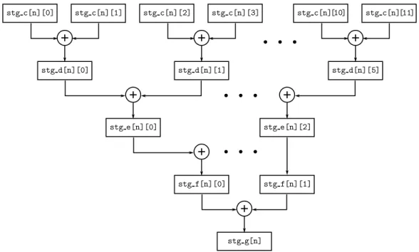
The last four stages of the filter sum the taps in a tree-like fashion. Figure 3-9 illustrates how the components of stg c sum to stg d, which in turn sum to stg e and then stg f and stg g.
3.5
Baseband Emulation Stage
The baseband emulation stage is reserved for special modifications applied to the baseband signal. This channel emulator tries to achieve an architecture capable of pluggable transformations, so this stage could easily allow for the addition of additive Gaussian white noise, signal mixing, or other modifications. In this specific imple-mentation, the baseband signal is not modified, however the hardware architecture makes it relatively easy to plug in modules that do so.
3.6
Variable Mixer
The final digital processing stage is the mixer, which mixes the baseband signals with a intermediate carrier frequency. The result is sent out via the DAC.
The nominal mix frequency is 120 MHz. That is, given a set of I samples xI and
Q samples xQ, the output signal is:
xmixed[n] = xI[n] cos ( 2πfm fs n) + xQ[n] sin ( 2πfm fs n) (3.9)
where fm is nominally 120 ⋅ 106Hz and fs continues to be 1 ⋅ 109Hz.
Why nominally? The mixer is the perfect opportunity to inject the effects of ∆fc
from Equation 2.8, as the entire spectrum can be shifted simply by adjusting fm.
fm becomes 120 ⋅ 106+∆fc.
Figure 3-10 demonstrates the result of mixing the anti-aliased I and Q to 120 MHz. The digital architecture utilizes a direct digital synthesizer (DDS) to generate the carrier wave, multiplies incoming samples by this wave, and sums the results in a fully pipelined operation.
−180 −160 −140 −120 −100 −80 −60 −40 −20 0 Rel. P o w er [dB] (Calculated)
Mixed
0 100 200 300 400 500 Frequency [MHz] −80 −70 −60 −50 −40 −30 −20 −10 0 Rel. P o w er [dB] (HW Sim ulation )Figure 3-10: Result of mixing anti-aliased baseband signal to 120 MHz. The overall SNR for the hardware implementation is around 60 dB, which, for the target appli-cation, is excellent.
Figure 3-11: Example of DDS output with varying phase ramps. As we change the slope of the phase ramp, we select more or fewer elements in a single period of the lookup table. In this example, the dotted line corresponds to samples marked with a × and has twice the slope of the solid line, which corresponds to the samples marked with a ◻. Clearly, we can see that the resulting × sine wave will have twice the frequency of the ◻ sine wave.
3.6.1
DDS Background Theory
There are many ways to generate sine waves digitally. The simplest method is through the use of a lookup table (LUT). With this method, a period of the sine function (or any periodic function) is stored to memory and a “phase” is applied as an input index into the table. The phase is then incremented and the next value of the function is determined. The input phase accumulates until it overflows back to the start of the periodic function.
The slope of this phase ramp therefore determines the frequency of the output wave. Figure 3-11 illustrates how different phase ramps result in different frequency outputs.
In continuous time, this concept is very simple. For a function f with phase input φ, the output of that function at a given phase is just f (φ). Furthermore, as we want successive values of f , we just update φ with some δφ continuously. This value determines the frequency. Things become more complicated as we enter the discrete time-domain realm. In this realm, we have a timestep τs instead of being in
having a phase that is all real numbers between 0○ and 360○. We now refer to the phase as ϕ and the change in phase at each timestep as ∆ϕ. In a digital system, it makes sense to make N a power of two such that we can always make ϕ simply by creating a register lg(Nt)bits wide (so that when it overflows, the phase starts at the beginning again).
Now, ∆ϕ becomes:
∆ϕ = fm⋅τsNt (3.10) ∆ϕ increment to phase with each timestep
fm desired target frequency to generate
τs timestep (inverse of sampling frequency)
Nt number of elements in the LUT
Unfortunately, unless the quantity on the right-hand side is a whole number, errors accumulate very rapidly as ϕ ← ϕ+∆ϕ with each timestep. As a result, the frequency that is actually generated will be inaccurate. One thing we can do that will sacrifice the purity of the signal (i.e. its precision) in favor of better accuracy is to make ϕ a fixed decimal value and only feed the integral part into the LUT. Thus, with each timestep update, we do not accumulate quite as much error. If we wish to introduce Nf decimal values, with Nf being a power of two, ∆ϕ becomes:
∆ϕ = fm⋅τsNtNf (3.11) Now, we simply take the upper lg(Nt)bits of ϕ and use that as the index into the LUT.
There are more techniques that one can use to improve the output signal quality in different ways. For example, one natural result of this method is that harmonics are generated. By dithering the value of ∆ϕ with a small random offset on each increment, one can suppress these harmonics at the cost of raising the signal’s noise floor.
3.6.2
Implementing a DDS
Using a fixed-point decimal notation with the integral and fractional parts both being powers of two makes it easy to separate the components in order to provide an index into the LUT. In this implementation, we set Nt to 210 (i.e. 1024 table entries) and
Nf to 216 (i.e. 16 bits of fractional precision).
The lookup table was implemented as a dual-read-port ROM with 18-bit values. This 1024 × 18 design fits neatly into a single Virtex 6 BRAM. On each clock cycle, one of these ports outputs a sine sample and the other outputs the corresponding cosine sample. A total of 8 of these LUTs were instantiated, one for each sample on the input bus.
The nominal mix frequency is fm =120 MHz. We can calculate ∆ϕ as follows:
∆ϕactual=fm⋅τsNtNf (3.12) =120 ⋅ 106⋅ 1 1 ⋅ 109 ⋅2 10 ⋅216 (3.13) =8053063.68 (3.14) ∆ϕ = ⌊∆ϕactual⌋ =8053063 (3.15)
Therefore, with each timestep, we add 8053063 to the existing register storing ϕ and use the top 10 bits of that value as the index into the LUT.
The difference between the actual and approximate phase increment, 0.68, is ex-ceptionally small, and produces a frequency error of only:
error = ∣∆ϕactual−∆ϕ ∆ϕactual
∣ (3.16)
=8.44 ⋅ 10−6% (3.17) or around 10 Hz.
Figure 3-12: Mixer Architecture.
3.6.3
Mixer Architecture
As illustrated in Figure 3-12, the architecture is a very simple 3-stage pipeline. In the first stage, the set of input samples is registered as well as their corresponding sine and cosine values in the LUT. In the second, the real component of the sample is multiplied by the cosine value and the imaginary component is multiplied by its corresponding sine value. Finally, in the third stage, they are summed.
3.6.4
Parallel Lookup Tables
One slight difference between a standard DDS implementation and that of this project is the need for parallel LUTs because there are 8 samples per clock cycle. As a result, we actually need 8 LUTs where we feed offsets of a phase into each one. Namely, if we’re starting at the beginning of the table, where ϕ of the first sample is 0, the ϕ of the next sample must be 0 + 8053063, etc.: Thus, we have an address input bus — a one-dimensional array whose starting addresses are:
[ 0 1 ⋅ ∆ϕ 2 ⋅ ∆ϕ 3 ⋅ ∆ϕ 4 ⋅ ∆ϕ 5 ⋅ ∆ϕ 6 ⋅ ∆ϕ 7 ⋅ ∆ϕ ] (3.18) Then, with each timestep, we add 8 ⋅ ∆ϕ to each of these values.
As mentioned, each LUT has two input ports. This allows simultaneous retrieval of sine and cosine values. The LUT itself is a single period of a cosine function. Therefore, we can retrieve a sine function simply by adding a three-quarter period to
the input phase. For a 1024-entry table, we would add 3
4 ⋅1024 = 768 to each input
phase to get the corresponding sine value.
3.6.5
Making the Mixer Variable
Previously, ∆ϕ, was a fixed value, as fm was set to 120 MHz. However, because the
dominant effect of Doppler shifting on a given spectrum is additive frequency change, it makes sense to alter the mixing frequency. From Equation 2.8, we now want to set fm=120 ⋅ 106+∆fc. Because ∆ϕ is a linear function of the desired mixing frequency, we can represent the term as follows:
∆ϕ = fm⋅τsNtNf (3.19) = (120 ⋅ 106
+∆fc) ⋅τsNtNf (3.20) =120 ⋅ 106⋅τsNtNf+∆fc⋅τ NtNf (3.21)
=∆ϕn+∆ϕd (3.22)
The latter term is the phase increment from the Doppler effect and the former is the nominal increment. Therefore, we generate ∆ϕd and add it along with ∆ϕn to ϕ
to generate the next phase input into the LUTs. Figure 3-13 illustrates the additional component of this architecture. This gives us a variable mixer, capable of applying the Doppler effect on an input spectrum.
3.7
DAC
The DAC chosen was the Texas Instruments DAC5681Z, which outputs 16-bit sam-ples at 1 GSPS at 1.0 Vpp. This particular DAC has a SINC output filter that
makes production of a signal within the third Nyquist fold impossible. As a con-sequence, the digital mixer mixes the baseband signal to the intermediate frequency (IF ) 120 MHz. An external analog mixer then mixes the signal to its final carrier fre-quency of 1.25 GHz.
Figure 3-13: Revised variable mixer architecture. The addition of the increment adjust input produces a variable mixer.
3.8
Analog Mixer
To upconvert from the IF to the carrier frequency, a simple analog mixer is used. For a spectrum centered around fm to be mixed up to one centered around fc, an analog
mixer is fed the local oscillator (LO ) fc−fm as well as the spectrum at fm. Then, a spectrum is produced at fc as well as fc−2fm. The frequency fm should be large enough so that the image produced on the opposite side of fc−fm is far enough away that it is rejected by the receiving modem’s internal passband filter.
3.9
Numeric Precision
There is an inherent trade-off between numeric precision and resource usage. All of the calculations involve decimal math. For example, the coefficients in the anti-aliasing filter are all fractions, as are sine and cosine values in the mixer.
Floating-point math is generally not chosen for most digital designs. To minimize unnecessary resource consumption, fixed-point math is generally preferred; thus, it was chosen for this project. Each stage of the signal chain is composed of an integer and decimal component. For example, a 16.8 representation would mean that the integer part was 16 bits wide while the decimal part was 8 bits wide.
the hardware multipliers in the FPGA fabric. The Virtex 6 has a large number of DSP48E1 slices, which include a pre-adder, a 25 × 18 multiplier, and an ALU. For resource-intensive operations, namely the anti-aliasing filter and the mixer, it would be useful to enforce the constraint that all multiplication inputs are no larger than 25 and 18 bits in width. Based on the layout of the FPGA fabric, in the case of both the AA filter and the mixer, lookup table values are pulled from BRAMs, which dump directly into the 18-bit multiplier inputs.
The input into the AA filter is a 12-bit integer from the ADC. To maintain as much precision as possible while keeping true to the 25-bit limit into the next multiplier stage, the output is 16.9. Table 3.1 lists the fixed-point representations of each stage.
Table 3.1: Numeric format of each signal chain stage’s output Stage Output’s Representation ADC Capture 12.0
DDC 12.0
Anti-Aliasing 16.9 Baseband Emulation 16.9
Chapter 4
Implementation of the Channel
Emulator
The channel emulator consists of two domains: the hardware domain processes a streaming input signal and the software domain directs the hardware how to process that signal. The two communicate via a custom protocol. Careful consideration went into the design of this implementation so that the channel emulator can be extended to emulate environmental effects beyond simple Doppler shifting.
4.1
Hardware Considerations
Transforming a signal sampled at 1 GSPS is not possible with a CPU, so the log-ical choice of signal processing device is a field-programmable gate array (FPGA). These devices are best described as blank canvases on which digital circuits of great complexity can be created. FPGAs are perfect for complex signal processing and massively-parallel computations. Creating a digital circuit for an FPGA starts with a behavioral description of that circuit using a hardware description language (HDL). In the case of this channel emulator, the language VHDL was chosen. Once the circuit has been fully described, it is synthesized and mapped into real logic using a software tool provided by the FPGA vendor. Finally, the result is routed onto the FPGA fab-ric and a programming file is created. The user can then program the FPGA with
this programming file and run their application.
4.1.1
FPGA Evaluation Board
Generally, for the purposes of prototyping, FPGA evaluation kits are used. These kits are full boards that provide useful frameworks for developing applications. In addition to having an FPGA fully routed on the board, they often feature a variety of peripheral hardware, such as USB UARTs, ethernet ports, digital video ports, and an array of buttons and switches for easy configurability.
This project used the ML605 evaluation kit from Xilinx. This board features a Virtex 6 FPGA, DDR3 RAM, high-speed connectivity, and a variety of other features. Xilinx also has excellent documentation for both the features of the FPGA and the components on the evaluation board.
The Virtex 6 family is Xilinx’s second-newest generation at the time of writing (and was the newest at the start of the project when hardware decisions were being made). This chip has a variety of useful functionality built into the fabric, and there are few particular features that make it highly desirable for this project. Because the device must operate at very high speeds in a streaming manner, the process of capturing data from the analog interface (described in Section 4.1.2) and sending the transformed signal back to that analog interface requires high-speed hardware sup-port. The Virtex 6 contains a number of high speed serializer-deserializer (SERDES ) blocks, which convert data between the narrow high-speed bus used to talk to the analog interface and a wide low-speed bus used to process data within the FPGA. This architecture is detailed in Sections 4.2.4 and 4.2.5. Along with these SERDES modules, the Virtex 6 family has clock routing and control features that make process-ing data across multiple clock domains relatively straightforward. These capabilities are instrumental in producing a real-time streaming signal processing environment.
The last major useful feature of the Virtex 6 layout is the large number of DSP48E1 slices. These are specific function blocks that contain a pre-adder, an 18×25-bit multi-plier, and an arithmetic logic unit. In particular, the hardware multipliers are of great importance to this project because they make the process of applying
com-plicated filters to high-speed signals possible. The particular Virtex 6 chip on the ML605 has 768 DSP48E1 slices; the final design of the emulator framework uses a relatively small fraction of them, about 15%. The rest can be used for the individual emulation modules that will come from future development.
4.1.2
Analog Interface
The channel emulator’s interface to the signal path is analog. Thus, to sample data for processing within the FPGA and then deliver that data to the output, an analog-to-digital converter (ADC ) and digital-to-analog converter (DAC ) were necessary. To reduce the development cycle time, a third-party add-on module featuring two ADCs and two DACs was purchased.
4DSP is a company that produces such add-on boards for FPGAs. These boards connect to the FPGA evaluation kit using the FPGA mezzanine connector (FMC ) pseudo-standard, which provides numerous high-speed connections to the FPGA. 4DSP produces a series of analog boards, but only one fit the suitable requirements: the FMC110. This board contains two ADS5400 ADCs and two DAC5681Z DACs, each operating at 1 GSPS. It also has an on-board clock generator to drive these chips as well as the digital interface to the FPGA.
4DSP provides a reference firmware that can be loaded onto the FPGA to test the features of the FMC110. It sets up the FPGA as a router between the FMC110 and a computer via the evaluation kit’s ethernet interface. A Windows program connects to the FPGA, drives a waveform to the DAC and captures a few thousand samples from each ADC. The source code for this firmware is also provided.
The reference firmware is based on a burst architecture: a finite of samples is read into a large buffer, which is then drained more slowly via ethernet to send the data back to the computer. A new design, built from scratch, was necessary in order to meet the real-time streaming requirements of the channel emulator. Components of 4DSP’s firmware were used for reference.
This channel emulator only uses one ADC and one DAC. There are plenty of re-sources on the FPGA available for further development of a second emulation channel
Figure 4-1: FMC110 architecture. Relevant components of the FMC110 architec-ture used by the channel emualtor are shown here.
using the other pair. Figure 4-1 illustrates the architecture of the FMC110, high-lighting the parts of the board that are used in the emulator. The ADCs, DACs, and clock generator are configured via their respective serial peripheral interfaces (SPI ). The high-speed data interfaces on the ADCs and DACs are parallel low-voltage dif-ferential signalling (LVDS ) buses, which consume the majority of the resources of the FMC connector. A configurable programmable logic device (CPLD ) acts as a router for configuring the devices with SPI interfaces. It also provides the capability to reset certain devices with asynchronous reset lines.
4.2
Digital Hardware Architecture
Figure 4-2 is a block diagram of the various hardware components that were imple-mented on the FPGA. The signal processing architecture described in Chapter 3 is a relatively small component of the larger system operating inside the FPGA.
4.2.1
Clocking
It is particularly important to note that there are numerous top-level clocks in the system. Table 4.1 describes their origin and purposes. Note that clocks with signals {p,n} are differential and are used to drive MMCM blocks on the FPGA to generate
Figure 4-2: Digital hardware architecture. Not shown are lesser components such as the PWM fan speed controller and debugging modules, which were later removed in the final design.
other clocks.
4.2.2
Picoblaze Microprocessor
After the FPGA starts up, the system must perform a series of configuration steps to initialize all of the on-board hardware. After the system has been configured, it can continue to receive additional configuration directives. It is common in most FPGA designs to include a small microprocessor on which to allocate portions of the design that are state-based, such as reading in a command string.
The Picoblaze is a very small soft-core microprocessor developed by Xilinx en-gineer Ken Chapman. While minimalistic, it provides the perfect feature set for configuration of various modules on the device.
Firmware for the microprocessor is written in assembly, assembled, and the re-sulting machine code is loaded into block RAMs on the FPGA. The firmware imple-mentation is discussed in more detail in Section 4.3.
4.2.3
SPI Controller
The FMC110 board is configured via a SPI bus. SPI commands sent to the board are interpreted by the on-board CPLD, which directs communication to one of the configurable chips on the device.
Table 4.1: System Clocks
Clock Name Freq. Source Main Uses
sysclk {p,n} 200 MHz FPGA Eval Board Generation of other board clocks
clk200 200 MHz sysclk {p,n} ADC IODELAY control clk125 125 MHz sysclk {p,n} virtually all processing
and control blocks clk50 50 MHz sysclk {p,n} fan PWM clock
generator pwmclk 25 MHz clk50 fan PWM clock adc0 clka {p,n} 500 MHz FMC110 input data clock
from ADC0
adc0 dout dclk 125 MHz adc0 clka {p,n} ADC0→FPGA output data samples
clk to fpga {p,n} 500 MHz FMC110 DAC input data dac0 din dclk 125 MHz clk to fpga {p,n} FPGA→DAC input
Figure 4-3: FMC110 SPI packet structure. SPI packets begin with a prefix that indicates which device the controller is intending to write to or read from. All devices except for the clock generator use an 8-bit address as shown in the upper diagram. The clock generator uses a 16-bit address as shown in the lower diagram.
To facilitate SPI communication with the FMC110, a SPI controller was built. The microcontroller firmware provides a set of subroutines that send data to output ports that are connected to the SPI controller, which, in turn, processes the SPI instruction. Figure 4-3 illustrates the structure of a SPI packet. The ADCs, DACs, and CPLD all have an 8-bit address space and the clock generator has a 16-bit address space; the SPI controller handles both cases.
Figure 4-4: FMC110 DAC controller architecture. The DAC controller uses an incoming clock from the FPGA to produce its own set of clocks for driving data flow. The serializer sends a data stream to the DAC, as well as a 1 GHz clock.
4.2.4
DAC Controller
Fundamentally, to drive the DAC, 16 bits of data must be fed in parallel output format at a speed of 1 GHz. Given that the FPGA itself operates at a speed of 125 MHz, achieving this design constraint is done by passing the data through several clock domains. Figure 4-4 describes stages of the DAC controller.
Clock Generation
The FMC110 provides a 500 MHz signal to the FPGA that is synchronized to the data-loading clock it internally routes to the DACs. This clock is divided into two new clocks: one at 250 MHz and one at 125 MHz named fmc clk d4 and fmc clk d8 respectively. The clock line fmc clk d8 is provided as an output from the module and incoming data must be aligned it.
8-to-4 FIFO
Data entering the module aligned to fmc clk d8 is sent into a FIFO whose read clock is fmc clk d4 and whose read port size is a quartet of samples. Thus, if the sample input at a given time was ⌞⟪A ⋅ B ⋅ C ⋅ D ⋅ E ⋅ F ⋅ G ⋅ H⟫⌝, then the outputs from the FIFO would be: ⌞⟪E ⋅ F ⋅ G ⋅ H⟫ → ⟪A ⋅ B ⋅ C ⋅ D⟫⌝.
Reordering and 4-to-1 Serialization
With data now formatted as quartets at 250 MHz, the data bits are reordered for input into a SERDES serializer, which produces individual samples aligned to the 500 MHz input clock at double data rate. These samples are sent out to the DAC via the FMC110 interface. Additionally, the serializer actually generates a 1 GHz clock (by alternating 1 and 0 bits at 500 MHz DDR) and sends that to the DAC as well.
4.2.5
ADC Controller
The ADC interface is somewhat the “opposite” of the DAC’s: serial samples at the hardware interface are converted to blocks of parallel samples synchronized to the FPGA’s system clock. However, it is somewhat more complicated in that its incoming data lines must be synchronized to the incoming clock using a delay-locked loop (this initialization phase is discussed in Section 4.3.4). Figure 4-5 illustrates the processing stages of the ADC controller.
The FMC110 delivers data on a supplied 500 MHz input clock. An MMCM pro-duces a 125 MHz clock. The incoming data is sent through a SERDES de-serializer whose output is an octet of samples aligned to the divided clock. The output is then sent through a FIFO in order to align the data to the FPGA system clock.
4.2.6
FIFO Dumper
To test and verify the operation of the ADC, a FIFO dump system was developed. When the CPU triggers the dumper to start, the output of one of the ADCs is redirected from going into the channel emulator’s signal chain to a very large FIFO (it was configured to take up almost all of the remaining BRAM on the FPGA). When the FIFO is full, the dumper takes control of the UART and sends its full contents out via the UART. A software script reads this data and unpacks it back to its 12-bits-per-sample representation.
Figure 4-5: FMC110 ADC controller architecture. The ADC controller fea-tures a DLL trainer that configures the de-serializer; its functionality is described in Section 4.3.4.
4.3
Configuring FMC110 Hardware
All of the devices on the FMC110 must be properly initialized. The overall startup process is as follows:
1. Configure the CPLD to set board-level settings.
2. Configure the clock generator to provide clocks to the ADCs, DACs, and FPGA. 3. Configure the DACs and have them perform a “training” phase so that they
can align their clock delay appropriately
4. Configure the ADCs and perform a training phase on the FPGA to align clock delays.
This startup process is driven by the CPU. Nearly 80 registers need to be set, making the startup code fairly involved. The startup takes around 10 seconds to complete.
4.3.1
Channel Emulator Configuration Interface
The Picoblaze Assembler has no support for macros, so a small interpreted language was designed to produce assembly code from a set of keywords. This program was named cci (channel emulator configuration interface). For example, if we wish to configure ADC0’s register 0x00 to have value 0xAA, then we would write as an input to cci:
fmcw adc0 00 AA
cci would then produce an assembly file containing the code: load s0, 00
load s1, AA call send_adc0
Appendix A describes the full syntax of the language and details how cci can be used to both generate assembly code and to perform on-the-fly configuration.
The channel emulator makes use of cci to generate the initialization routine which brings up all of the chips.
4.3.2
Configuring FMC110’s CPLD and Clock Generator
After the CPU has started, it jumps into the FMC110 initialization routine, which configures the CPLD to reset the clock generator and use an internal clock source. It also resets the DACs. Next, it configures the clock generator, which provides stable, phase-corrected 500 MHz clocks to each ADC and DAC, as well as one to the FPGA. The routine then waits for the PLL on the clock generator to lock before proceed-ing to configure the DAC.
4.3.3
Configuring DAC0
The DAC is configured to provide a two’s complement output and the FPGA is then configured to provide a stable data clock to the DAC. The DAC’s DLL is then reset
and the CPU waits until the DAC reports that its DLL has been locked. This process guarantees that the DAC has synchronized to the data clock that the FPGA provides along with the input data stream.
Once the DLL has locked, the FPGA provides a checkerboard pattern of data: a stream of 0xAAAA, 0x5555, 0xAAAA, etc. It then reads the DAC error register to confirm that no errors in the checkerboard pattern were received. This stage ensures that the data going into the DAC is correctly aligned to the data clock.
Following the training period, the CPU reports if there were any errors in testing by reading the error register of the DAC. It then enables the DAC for standard operation (streaming data output).
4.3.4
Configuring ADC0
Finally, the CPU configures the ADC for operation. Before the input data stream can be considered valid, the ADC controller must undergo a training phase, which ensures that each incoming data bit is aligned to the incoming clock. Because the data is being sent from the ADC extremely quickly, the length of the traces can affect propagation time. It is possible for the clock to become skewed from the data, which would cause the data to sometimes appear invalid. To overcome this, a delay-locked loop is available for every incoming bit in the sample stream. In the training phase, the ADC is configured to produce a pseudo-random bit sequence (PRBS ) with the function x7+x6+1. The training system calculates the same PRBS on the FPGA
and compares the result to what it receives from the ADC. When it receives incorrect data, it adjusts the SERDES delay timing and tries again.
Finally, the CPU confirms the validity of the ADC input by configuring it to send a checkerboard stream (0xAAA, 0x555, 0xAAA. . . ) and tests for received values that deviate for the pattern. After a few seconds of testing, it reports back the number of times it discovered an error.
The CPU sets the ADC to run in normal mode and at that point, initialization is complete.