by
Peter Mayer
Submitted to the Department of Electrical Engineering and Computer Science
in partial fulfillment of the requirements for the degrees of
Master of Engineering in Electrical Engineering
and
BARKER
Bachelor of Science in Physics
at the
MASSACHUSETTS INSTITUTE OF TECHNOLOGY
Feb 2002
MA SSACHUSETTS INSTITUTE OF TECHNOLOGYJUL 3 1 2002
LIBRARIES
I
C
@ Peter Mayer, MMII. All rights reserved.
The author hereby grants to MIT permission to reproduce and distribute publicly
paper and electronic copies of this thesis document in whole or in part.
Author ...
Department of Electrical hngineering and CdTnAputer Science
February 10, 2002
ertified by...-.
.
-ajeev J. Ram
ssociate Professor
Thesis Supervisor
Accepted by ... ... ...Arthur C. Smith
Chairman, Department Committee on Graduate Students
2
Current Fluctuations in Semiconductor Devices
byPeter Mayer
Submitted to the Department of Electrical Engineering and Computer Science on February 10, 2002, in partial fulfillment of the
requirements for the degrees of
Master of Engineering in Electrical Engineering and
Bachelor of Science in Physics
Abstract
Current fluctuations in semiconductor devices are important for both practical and funda-mental reasons. Measurements of the current noise in devices can establish fundafunda-mental limits on the attainable signal-to-noise ratio in communication links and can also provide insight into the basic physics of the device's operation. This work presents a suite of cur-rent noise measurement techniques useful for studying a range of devices. These techniques are applied to investigate the extent to which the photon noise from lasers biased in the same circuit is correlated due to the current noise in the shared bias currents. The first measurements of the circuit-induced photon noise correlations in semiconductor lasers are presented. A calibrated measurement of the photon noise of a single laser as a function of its bias current is also presented.
Thesis Supervisor: Rajeev J. Ram Title: Associate Professor
Acknowledgments
There are several people without whom this thesis would not have been possible. My advisor Professor Rajeev Ram has been a constant source of support. His unique gift of understanding and explaining complicated phenomena with simple clarity was often called upon, and his contagious enthusiasm for research was invaluable. Mr. Fahan Rana was my principal collaborator on this work, and is responsible for the theory of noise in lasers which was used in this thesis. Fortunately for me, his incredibly deep knowledge of physics was matched by his patience in explaining things, and I leaned on his knowledge frequently. Mr. Harry Lee has been involved in my research in one way or another since I joined this research group. Harry has the dubious distinction of being the firefighter, the guy who I can go to to fix anything. I cannot list all of the ways in which I have depended on his expertise.
I have confined myself in these acknowledgements to only addressing my debts to people which are most immediately related to the content of this thesis. More valuable to me than any of the work I have done are the people I have worked with. Some of these friendships are very old, and some are relatively new, but each means more to me than I feel capable of expressing in words.
I must break this rule to thank some people who did not have make technical
contribu-tions to this thesis, but who at times entirely sustained me. My mother and father have been a firm, unwavering source of support throughout my life. They taught me everything
I really need to know. Their honest, simple approach to life is my ideal. In a thesis about
electrical measurements, an analogy seems appropriate: they are my ground.
There is one more person who should certainly be thanked here, but I can't think of how to do it. With luck, I will have the rest of my life to thank her properly.
1 Introduction 15
1.1 Introduction . . . . 15
1.2 Measuring and Characterizing Noise . . . . 17
1.3 Noise in a Fiber Communication Link . . . . 22
1.4 Link Slope Efficiency and the SNR . . . . 25
1.5 Thermal Noise . . . . 27
1.6 Thesis Outline . . . . 30
2 Theory of Electrical System Noise Modeling 31 2.1 O verview . . . . 31
2.2 One-port Equivalent Circuit Models . . . . 32
2.2.1 Resistors, Capacitors, and Inductors . . . . 32
2.2.2 D iodes . . . . 35
2.3 Two-port Equivalent Noise Models . . . . 38
2.3.1 Transistors . . . . 38
2.3.2 Transformers . . . . 41
2.4 Theory of One-ports and Two-ports . . . . 41
2.4.1 One-port Thermal Noise . . . . 42
2.4.2 Generalized Two-port Noise Models . . . . 42
2.4.3 Multiple Amplifier Stages (Friss's Formula) . . . . 48
2.4.4 Optimum Noise Resistance . . . . 49
CONTENTS
2.5 External Low Frequency Sources of Noise . . . . 51
2.6 Summary . . . . 57
3 Current Noise Measurements 59 3.1 Summary of Instruments . . . . 59
3.2 Measurement Equipment . . . . 60
3.2.1 Low Noise Current Preamplifier . . . . 60
3.2.2 Low Noise Voltage Preamplifier . . . . 63
3.2.3 Low Noise Transformer Preamplifier . . . . 64
3.2.4 Data Aquisition System . . . . 65
3.3 Johnson Noise Measurements . . . . 70
3.3.1 Calibration . . . . 71
3.3.2 Noise Thermometer . . . . 76
3.4 High Impedance Measurement . . . . 79
3.5 Low Impedance Measurement . . . . 83
3.5.1 New Difficulties . . . . 83 3.5.2 Two Solutions . . . . 86 3.5.3 Transformer-Coupled Measurement . . . . 86 3.5.4 Calibration . . . . 88 3.5.5 Measurement . . . . 90 3.6 Conclusions . . . . 92
4 Circuit-Induced Laser Noise Correlations 93 4.1 Semiconductor Laser Diodes . . . . 95
4.1.1 Theories of Diode Noise . . . . 95
4.1.2 High-Impedance Supression of Noise . . . . 96
4.1.3 External Current Correlations . . . . 97
4.2 Correlation Setup . . . . 102
4.2.1 The Transimpedance Preamplifiers . . . . 104
4.2.2 Low Frequency Sensitivity vs. 4.2.3 The Photodetectors... 4.2.4 The Lasers . . . . 4.3 Measured Single Laser Fano Factor . 4.3.1 Calibration . . . . 4.3.2 Measurement and Results 4.4 Correlation Measurement... 4.4.1 Preliminary Measurements 4.4.2 Correlation Measurement 4.5 Summary . . . .
Microwave Measurement Sensitivity . 105 . . . . 10 6 . . . . 10 7 . . . . 10 9 . . . . 1 10 . . . . 1 1 2 . . . . 1 14 . . . . 1 1 6 . . . . 1 19 121
5 Conclusions and Future Directions
5.1 Summary and Conclusions . . . .
5.1.1 M odeling . . . .
5.1.2 Current Noise Measurement Techniques . . . . 5.1.3 Photon Correlations in Circuit-Coupled Lasers
5.2 Directions for Future Work . . . .
A Current Noise in a Resonant Tunneling Diode
A.0.1 Tunnel Junctions at DC
[1]
. . . . A.0.2 Mesoscopic Noise [2] . . . .A .0.3 N oise in RTD s . . . .
B Basics of Semiconductor Lasers
B.1 Semiconductor Laser Structure . . . . B.2 Carrier Recombination and Light Generation . . . .
B.2.1 Laser Rate Equations . . . . B.3 Solution of the Rate Equations for Low Frequencies . . . .
C Matlab Code 123 . . . . 123 . . . . 123 . . . . 124 . . . . 126 . . . . 126 131 132 135 139 143 143 145 146 147 151
1-1 The definition of the relative intensity noise (RIN). . . . . 1-2 The two alternate circuit representations of a resistor's thermal noise. . . . 1-3 A digital optical fiber link .. . . . .
1-4 The conditional PDFs of the output voltage for a "1" input and a "0" input.
1-5 L-R circuit with Langevin voltage noise source. . . . . 2-1 One-port noise model of a resistor. . . . .
2-2 One-port noise model of a capacitor. . . . .
2-3 One-port noise model of an inductor. . . . . 2-4 One-port noise model of a diode. . . . .
2-5 Two-port noise model of a bipolar junction transistor.
2-6 Two-port noise model of a field effect transistor. . . . 2-7 Two-port noise model of a transformer. . . . . 2-8 Two-port noiseless model of an operational amplifier..
2-9 General noiseless model of a two-port network... 2-10 General two-port network with voltage noise sources at 2-11 General two-port network with input referred noise. .
2-12
2-13
2-14
2-15
Balanced detection scheme for the measurement of sma Measurement with noisy voltage amplifier. . . . . Capacitive coupling of noise into a measurement. . . .
Capacitive coupling of noise into a current measuremen
. . . . 32 . . . . 34 . . . . 34 . . . . 35 . . . . 38 . . . . 39 . . . . 4 1 . . . . 43 . . . . 43
the input and output. 44 . . . . 45 11 signals. . . . . 46 . . . . 49 . . . . 52 t . . . . .
53
9 20 21 23 25 28LIST OF FIGURES
2-16 Correct and incorrect shielding of a sensitive measurement. . . . . 55
2-17 Inductive coupling of noise into a measurement. . . . . 55
2-18 Microphonic coupling of noise into a measurement. . . . . 56
3-1 Two-port model of a current amplifier. . . . . 62
3-2 Two-port model of a voltage amplifier. . . . . 64
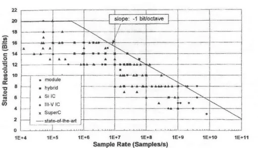
3-3 Resolution and bandwidth of analog-to-digital converters (1999). . . . . 66
3-4 Transfer function of ideal DAQ. . . . . 67
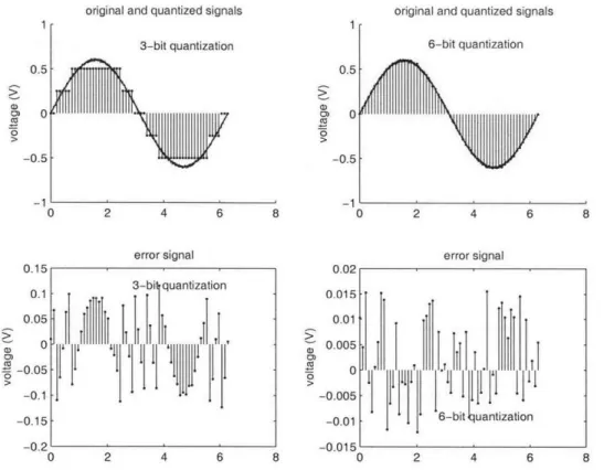
3-5 Original, quantized, and error signals for 3-bit and 6-bit quantization. . . . 68
3-6 Experimental setup for Johnson noise measurements. . . . . 70
3-7 Experimental setup for room temperature Johnson noise measurements. . . 71
3-8 Transfer function of amplifier chain. . . . . 73
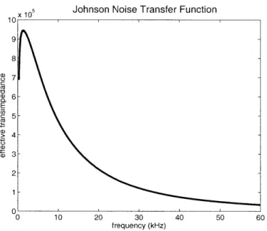
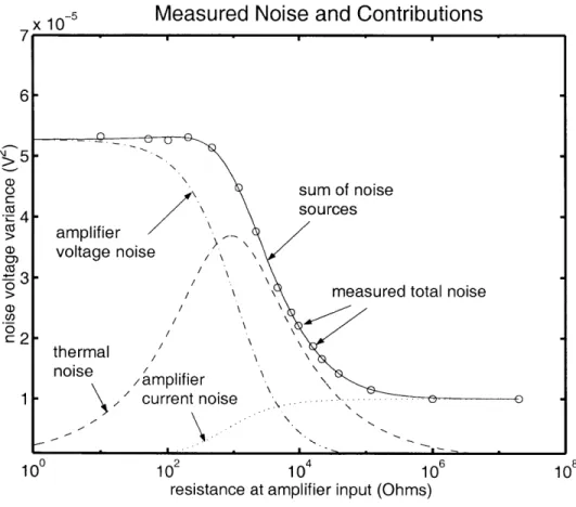
3-9 Measured noise with different source resistances, and theoretical contribu-tions to the noise obtained with a curve fit. . . . . 75
3-10 Noise power measured as a function of temperature. . . . . 78
3-11 Noise measurement and calibration scheme for photodetector optical noise m easurem ent. . . . . 80
3-12 Noise measurement and calibration scheme for photodetector optical noise measurement, written to emphasize symmetry of the signal generators. . . . 81
3-13 DUT for calibration circuit, with parasitic capacitance. Also included are the Thevenin equivalent source and impedance values. . . . . 82
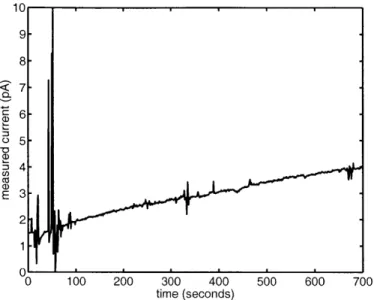
3-14 M easured Fano factor. . . . . 83
3-15 inferred fundamental charge over valid frequencies. . . . . 84
3-16 Low-frequency noise model of a diode. . . . . 85
3-17 Transformer-coupled noise setup. . . . . 87
3-18 Results of parameter extraction from I-V curve. . . . . 90 3-19 Transfer function of the transformer-coupled measurement with diode DUT. 91 3-20 Measurement of diode shot noise using transformer-coupled measurement. . 92
4-1 One-port noise model of a diode. . . . . 94
4-2 Pump supression in a diode laser. . . . . 96
4-3 Four simple bias circuit topologies. . . . . 98
4-4 The correlated photon noise measurement setup. . . . . 102
4-5 Laser characterization curves. . . . . 108
4-6 The calibration measurement setup at high frequencies. . . . . 109
4-7 Measured transfer functions needed for calibrated photon noise measurements. 112 4-8 Power spectrum of the measured voltage noise, taken at Ibias = 81 mA. . 113 4-9 Power spectrum of the photodetector current noise, taken at bias = 81 mA. 114 4-10 Photodetector current and incident light Fano factors as a function of laser b ia s. . . . . 1 15 4-11 The correlated photon noise measurement setup. . . . . 116
4-12 Spurious correlation between two lasers voltage biased in separate circuits. . 117 4-13 Spurious correlations measured with one laser off. . . . . 118
4-14 Noise correlation measured for lasers in 4 different circuits. . . . . 120
4-15 Possible mechanism for spurious correlation in circuits (B) and (C). . . . . 121
5-1 The four measured bias circuit topologies. . . . . 127
5-2 One-port noise model of a diode. . . . . 128
A-1 A practical realization of an RTD, and a schematic representation of the structure [3]. . . . . 132
A-2 A schematic energy level diagram for an RTD in the unbiased and biased case, showing the well density of states. . . . . 133
A-3 A typical I-V curve of an RTD. . . . . 134
A-4 A 1-D channel connecting two reservoirs, showing orthogonal occupied and unoccupied transmission states. . . . . 136
A-5 A 1-D channel connecting two reservoirs at low temperature and with an applied voltage bias. . . . . 138
12 LIST OF FIGURES
B-1 Basic structure and operation of a laser. . . . . 143 B-2 Important radiative processes in a semiconductor laser. . . . . 145
3.1 Performance of the SR570 low noise transimpedance amplifier. . . . . 61
3.2 Performance of the SR554 transformer amplifier. . . . . 65
3.3 Best fit param eters. . . . . 76
3.4 Best fit parameters for the measurement of Chen and Kuan
[4].
. . . . 764.1 Key specifications of the Analog Devices OP-27 operational amplifier used for the m easurem ent. . . . . 104
4.2 Key specifications of the photodetectors used for the measurement. . . . . . 107
4.3 Key specifications of the lasers used for the measurement. . . . . 108
4.4 Average measured spurious correlation with one laser off. . . . . 119
4.5 Average noise correlations. . . . . 119
Introduction
1.1
Introduction
Understanding current fluctuations (also called current noise) in semiconductors is impor-tant for practical and fundamental reasons. The most imporimpor-tant practical reason is that the fluctuations often fundamentally limit the device's signal-to-noise ratio. In most sys-tems in which information must be extracted from an analog electrical signal, current noise plays a part in setting the specifications of the devices [5], [6], [7], [8]. With the continued
shrinking of the MOS transistor and the resulting smaller signal levels, noise will become more important in the digital realm as well. Understanding noise's origins, how it can be modeled, and how it propagates through a complex system is essential to modern device design. Noise has also proven valuable as a test of quality and reliability in many devices, since it is highly sensitive to impurities and defects.
Aside from practical considerations, the measurement of current fluctuations in semicon-ductors provides a way to study interesting physics in the device. The easiest access to the physics of a device is provided by DC response curves such as the I-V (current vs. voltage) curve for electron devices and the L-I (light intensity vs. current) curve for light-emitting structures. However, at the price of a slightly more challenging measurement, studying current fluctuations often yields more useful information about the underlying physics of a
CHAPTER 1. INTRODUCTION
device than a DC measurement [9]. There are several reasons for this.
In any device, there is always some 'white' noise superimposed on a DC biased device (noise is called white if it has equal power over a wide range of frequencies, in analogy with white light). The presence of some of this noise in any dissipative system is a necessary consequence of the fluctuation-dissipation theorem [10]. Shot noise, noise resulting from the discreteness of charge in a biased device, also contributes white noise. A measurement of these simple noise sources generally would not yield more physical information than
DC measurements. However, because the white noise is filtered by the dynamics of a particular device, measuring the device's current noise is a way to examine the microscopic dynamics of the device. A practical example of this technique is the determination of the relaxation-oscillation frequency of a laser diode, a measure of the rate at which the laser's light can be modulated with an AC current [11]. This measurement can be performed
by simply examining the current noise spectrum of the device with a DC bias. It is not
necessary to modulate the current driving the laser, or detect the emitted laser light. This is a particularly useful measurement for lasers emitting at wavelengths for which fast or sensitive detectors do not exist.
Current fluctuation measurements can also provide information about mesoscopic charge transport, since interactions between charge carriers either through Coulomb repulsion or through the Pauli exclusion principle result in correlated motion of the electrons, altering the noise of the device [12]. Such many-body effects are generally not reflected in the DC response curve of a device. In addition, noise is a very sensitive probe of many forms of scattering. In many devices the noise at low frequencies (called 1/f noise for the shape of its power spectrum) has been found to be strongly correlated with the impurity concentration of the device. Thus noise is often a measure of the electrical quality of a fabricated device. This thesis develops a suite of techniques for measuring low-frequency current fluctua-tions in semiconductor devices and reviews the theory necessary for designing these mnea-surements. In general, noise measurements can be divided into frequency and time domain methods. The former is common in the literature [13] [14] [15] [16], and relies on a frequency
measurement of the noise using a microwave spectrum analyzer and a low noise amplifier.
A time-domain setup relies on sampling and quantization of a time signal to measure
low-frequency noise (<1 MHz). In many cases, this method allows for greater accuracy and flexibility than the standard RF techniques. In this thesis, the focus is on time domain measurements. Several setups are designed to allow the measurement of noise from devices of varying impedance. These methods are then applied to make the core measurements of this thesis. First, the photon noise from a heterostructure semiconductor laser diode is mea-sured as a function of bias. Second, the correlations introduced into the photon streams of series and parallel electrically coupled laser arrays are measured. Both results are analyzed in the context of current theory.
In general, the challenges in designing these measurements fall into three basic categories. First, the noise from the measurement apparatus which inevitably pollutes the measurement of device noise must be minimized. Second, the exact contribution of the test device's noise to the total measured noise must be measured, and the other unrelated noise subtracted out. Finally, a measurement and calibration method must be found to match both low and high impedance devices. The noise measurement methods described in this thesis will be discussed here in a broad context so as to aid readers in the custom design of noise measurement systems.
In the remainder of this chapter, a general introduction to the subject of current noise in semiconductor devices is given. The various measures used to describe noise are defined, and the basic classes of noise measurement techniques are described. To motivate the practical importance of noise considerations and to demonstrate the analysis of a system's noise budget, the noise in a fiber communication link is discussed. Finally, the Langevin formalism is introduced to derive the spectral density of the thermal noise of a resistor.
1.2
Measuring and Characterizing Noise
The fluctuations in the current measured through a device generally contain contributions from the motion of large numbers of interacting charge carriers. Modeling such a
sys-CHAPTER 1. INTRODUCTION
tem deterministically is impossible, so current fluctuations are treated mathematically as stochastic processes. All information about a general stochastic process is contained in the joint probability distributions (PDFs) for the process at all possible times. There is no easy
way to measure these PDFs in general, and in most practically interesting cases there is no need for such an exhaustive measurement. Many physically interesting random processes are characterized entirely or chiefly by the first and second order moments of their PDFs, so that the others may be neglected. The measurable quantities of these are the mean, the variance, and the autocorrelation function.
A simple way to obtain information about the first and second moments of an unknown
process is to repeatedly measure the fluctuating signal at small time intervals. Such a mea-surement is called a time-domain technique. The samples of the random process should be taken with time separations much shorter than the time span for which the autocor-relation function shows interesting structure. The mean, variance, and autocorautocor-relation of the process are then easily computed. Often performed with a sampling oscilloscope, the measurement is attractive for its simplicity and its general applicability, but is limited by the sampling speed of the measuring instrument. Many physical processes of interest occur over time scales shorter than a nanosecond, which is too fast to be accurately measured by modern time-domain sampling techniques.
Other measurements characterizing the first and second moments of the random process are performed in the frequency domain. To connect the time and frequency domains for a deterministic signal, one typically relies on the Fourier or Laplace transform
[17].
However, the Fourier and Laplace transform of a stochastic processes are not well defined[18].
Adifferent route to the frequency domain is through the Wiener-Khinchine theorem, which states that the autocorrelation of a time signal and the power spectral density (PSD) of the signal are related through the Fourier transform. The PSD can alternately be viewed as the result of a measurement of the RMS power in small frequency bins at every frequency. This is exactly the job of a spectrum analyzer, the work-horse of frequency domain measurements. Spectrum analyzers which can measure signals in the tens of gigahertz range are readily
available today. However, because microwave spectrum analyzers are usually operated in an environment matched to 50 Q, there is a best-case noise floor set by the thermal noise of a 50 Q load. Time domain measurments are free of this constraint, and can often be optimized for better noise performance than a comparable microwave system, depending on the specific details of the circuit. More will be said about this in Chapter 4.
The metrics used to describe noise vary. In theoretical discussions, noise is typically modeled as an instance of some random process. Starting with an understanding of the basic probability distributions of the noise process, the noise's autocorrelation and power spectral density can be derived. An example of this is found later in this chapter, when the power spectral density of the noise in a 1-D quantum channel is derived. When describing unwanted noise in practical analog systems, the relevant quantity is generally the signal to noise ratio (SNR), defined as the RMS power of the signal divided by the RMS power of the noise:
SNR - -V(Psignai(t)2) (Pnoise (t)2)
For zero mean signals, this reduces to the ratio of the variance of the signal to the noise process. The SNR is more commonly expressed in decibels:
SNRdB = 10log10(SNR) (1.2)
One point of possible confusion should be clarified. When discussing electrical current signals, the SNR is a ratio of mean square electrical currents. Equivalently, the SNR for the electrical signal is a ratio of electrical powers. When dealing with light, the SNR is a ratio of mean square optical powers. This is because in light-wave systems, signals are typically measured in power, whereas in a circuit, current or voltage are generally the signals.
When describing noise in a digital communication channel, the preferred metric for noise is the bit error rate (BER). The BER is the ratio of the average number of bits transmitted incorrectly per unit time to the average total number of bits transmitted per unit time. In practical digital fiber systems, bit error rates of 10-9-10--" are commonly required [19].
CHAPTER 1. INTRODUCTION
For more specific applications, there are other noise metrics. The relative intensity noise (RIN) is of interest because it is the accepted way to describe noise in lasers. It is defined as the mean square noise power divided by the mean square average power level. In general, the noise is white within the communication band so that the noise can be characterized with a certain power per 1 Hz of bandwidth. Expressed in decibels, a typical value for the RIN in a modern communication system is between -130 dBm and -140 dBm
[19].
Fig. 1-1[11] illustrates a noisy analog light signal with a mean power level Pave, a signal power Pmod,
and some rms noise power
a.
The SNR and the RIN for this signal are given by:P(t)-PaveP modSin((ot) P(t) Pmod P ave t
Figure 1-1: The definition of the relative intensity noise (RIN).
SNR _((Pmod sin(Wt))2) mod (1.3)
o 2
RIN = -" (1.4)
Pave
Given the modulation index m Pmod/Pave, the RIN and the SNR can therefore be easily related. Later in this section, a relation between the RIN and the BER is derived for a simple communication channel.
When modeling noise in electrical circuits at low frequencies, it is customary to use noise generators
[20].
These are idealized current or voltage sources whose output is a stochastic process in time, generally with a mean value of zero, a Gaussian distribution, and a white spectrum. Because the variance of true white noise is not well-defined (due to the finite signal power over an infinite bandwidth), these generators are typically specified with a value in units of Volts/v' Hz or Amps/v Hz. In electronic circuits, the noise power across any two ports can be represented as a noise current (voltage) generator in parallel (series) with the Thevenin resistance of the network defined by the two terminals, as shown in Fig. 1-2. A more careful description of the noise models for circuit elements is given in Chap. 2.RT
Figure 1-2: VTh =Th RT + ThRT
-0 tw aThe two alternate circuit representations of a resistor's thermal noise.
In microwave and RF circuits, a simplification of the low frequency description given above is possible due to presence of a universal input and output line impedance (typically
50 Q). In this case, a single number, such as the SNR, is used to characterize the noise at
a node in the circuit. Likewise, a single number known as the noise figure (NF), is used to characterize the change in SNR between the input and the output of a device. The NF of a device is given by:
SNR~ NF = 10 log1o SNRin
SNROut (1.5)
CHAPTER 1. INTRODUCTION
of the device is assumed to be the thermal noise associated with a 50 Q resistor. Typical noise figures for low-noise room temperature RF amplifiers are between 1 and 3 dB. Note that when describing the noise performance of a device in a circuit not impedance matched to 50 Q, the impedance looking out from the device's input must be specified for the NF to have meaning. More will be said about these issues in Chapter 2.
1.3
Noise in a Fiber Communication Link
To understand how noise enters and affects a practical system, consider the direct detection of a fiber optic signal. Noise present in the incident light beam and noise introduced in the detection process combine to set a fundamental limit on the accuracy of the received signal, quantified here by the bit error rate at the receiver.
A direct detection receiver typical of those used in fiber optic communication links [8] is
shown in Fig. 1-3. Digital data is transmitted using light of frequency v through the fiber link using a simple on-off keying format. The light signal intensity L,(t) is assumed to take the values Lo and L, with equal probability. Superimposed on the signal is some noise with intensity L,(t). This light signal is transduced into current using a PIN diode photodetector with a quantum efficiency r, an area A, and a bandwidth Av. The quantum efficiency is the average number of electrons generated for each incident photon. The resulting current signal is gained up by an amplifier with a transimpedance of R and, for simplicity, a bandwidth equal to that of the detector. The amplifier will always contribute some noise to the input signal, modeled here as a noise current generator Ian (t) placed across the input of the amplifier. Methods of modeling noise from amplifiers will be discussed in more detail in chapter 2. The output voltage from the signal alone is V(t), and the output voltage from the noise is V,(t). The output signal voltage V1(t) can take on values of Vo or V corresponding to the input light signal levels of Lo and L1. Finally, the output voltage (the sum of the output signal voltage and the output noise voltage) is fed into a comparator which interprets the signal as a one or zero depending on whether it is greater or less than some threshold voltage.
R
L-
--F_ +
optical --- an +
Figure 1-3: A digital optical fiber link.
For simplicity only amplitude noise is considered in this simple model, and uncertainties in the timing of the pulses are neglected. If a photon in the incoming stream of light has an arrival time independent of the others (so-called Poissonian statistics), then two principal contributions to the output noise voltage V(t) can be expected: the noise present in the light L, and the current noise Ian (t) from the amplifier. The noise present in the incident light signal L, is shot noise, due to the signal's Poisson statistics. This is generally a good assumption in practical communication systems, especially if the link between the receiver and the source is lossy. The noise L,(t) is transduced by the photodiode into current noise In(t) - L,(t) Aq. Here Ln(t)A is simply the number of noise photons incident on the detector per unit time. The signal L,(t) is similarly transduced into a current 1 (t) = L, r/qq. This current signal is then tranduced by the amplifier into a voltage V(t) = Is(t)R. The two current noise sources at the amplifier's input are similarly transduced into output noise voltage noises V1, (t) from the incident light and Van (t) from the amplifier noise.
Both V1,(t) and Van(t) can be modeled as random processes. Because it was assumed
that each photon arrival was independent of other photon arrivals, In (t) is a Poisson process with mean I(t). Its variance is therefore:
2
CHAPTER 1. INTRODUCTION
At the output, this results in a voltage noise:
a = 21(t)RqAv = 2V(t)qAv (1.7)
The variance of Ian(t) is determined by the internal details of the amplifier (see Chapter 2), and is typically given by some a
a,
giving rise to an output voltage noise variance of:2 _ 202
UVa = R2 a (1.8)
Since the light and amplifier noise sources are statistically independent of one another, their variances can be summed to calculate the total variance of the output noise voltage:
2 = o a + o7 (1.9)
The plot in Fig. 1-4 depicts the PDFs of the total output signal V(t) + V"(t) for the case when a zero and a one are transmitted. In general the variance of the PDF given that a '0' was transmitted can be different from the variance of the PDF given that a '1' was transmitted. Call these ao and a1, respectively. The output signal is sampled at discrete times, once per bit. To optimize the performance of the receiver, a threshold voltage V'h must be determined. If a voltage above V'h is sampled, the signal is recorded as a one; otherwise, the signal is recorded as a zero. The optimum cutoff voltage minimizes the probability of error, which is equal to the sum of the two shaded areas in Fig. 1-4 (with each area weighted by the probability of receiving a one or zero). A reasonable (but not quite optimal) choice for a cutoff voltage is the intersection of the two Gaussian curves. This voltage is given by:
Vin- a 0o1 1 + u1V0 (1.10)
Oo + or1
If
Q(X)
= exp(4)
dy, the shaded area under the Gaussian can be calculated to find the bit error rate:V1 - V Oro + (T 24
probability density
probability density
function if a 'O' was
function if a '1' was
transmitted
transmitted
probability
of error
V
0
V V VFigure 1-4: The conditional PDFs of the output voltage for a "1" input and a "0" input.
In the preceeding discussion, the BER of a system and the statistics of a system's fundamental noise sources were connected. The basic method can be extended to account for more complicated communication protocols or detection schemes [6],[21],[22].
1.4
Link Slope Efficiency and the SNR
During the discussion of the noise in a fiber link given in the previous section, the noise in the photons incident on the photodetector was assumed to be shot noise. This was done mainly to avoid involving a more detailed noise model for the photons emitted from the laser into the discussion; in a real link, the noise can be many times shot noise, and may or may not even be set by the laser's intrinsic noise. But in any case, the noise which degrades the signal to noise ratio of an optical link does not typically scale with the modulation
CHAPTER 1. INTRODUCTION
power of the signal, but rather with the average output of the laser, or with some other unrelated source (e.g. thermal noise in the modulation circuit). In such a sitiiation, one way to improve the SNR of the link is to increase the link slope efficiency.
In a microwave analog link, the link slope efficiency is the small signal gain between the modulated current driving the laser (or external modulator) and the small signal output current at the receiving photodiode. If we confine the discussion to links whose components are impedance matched to 50 Ohms, the link slope efficiency for a simple link of the type discussed in the previous section is simply the product of the laser slope efficiency and the photodetector slope efficiency, where the photodetector slope efficiency is assumed to include any optical loss in the link. Clearly, the best possible link slope efficiency for such a setup is 1, and this is often difficult to achieve. This limit is physically set by the simple fact that for every electron which is injected into the laser as part of the modulation current, at most one photon is emitted; at the photodetector, at best one electron of modulation current results from this incident photon.
Several schemes have been proposed for improving the link slope efficiency [23]. One proposal is to use a series cascade of lasers. In this scheme, a single electron is capable of producing multiple photons (one photon from each laser). Using a series array of discrete lasers, efficiencies of greater than
1
have been attained [24]. By epitaxially growing the lasers together and coupling them using tunnel junctions, one can overcome many of the bandwidth-limiting parasitic issues associated with the series discrete lasers, and still see enhanced slope efficiencies. The bipolar cascade laser, a working prototype of this concept useful for fiber links, has recently been demonstrated [25]. A pressing theoretical andexperimental question associated with this approach is to what extent the added link slope efficiency improves the current-to-current link SNR.
To calculate the theoretical SNR in a series cascade of N lasers, one might reason that total signal could be found by adding the magnitudes of each of the N individual laser signals in phase. To find the total noise from the N lasers one would add the variances of the N individual noise signals, assuming each laser's noise is independent of the other lasers' noise.
This would give a = vN improvement in the SNR compared to a single laser. According to this simple reasoning, by adding more series laser stages one can achieve arbitrarily high SNR. Of course the real world is not so kind, and there are several ways in which this analysis fails to hold. One fundamental error of the calculation is the assumption of totally independent noise sources. In this thesis, this assumption is investigated experimentally by measuring the correlation between the light of series and parallel coupled lasers. To the extent that this light is correlated, the noise contributed by each must not be considered independent.
1.5
Thermal Noise
One fundamental source of noise in practical systems is thermal noise. Thermal noise is present in every dissipative system. In their seminal paper, Callen and Welton
{10
showed that fluctuation and dissipation are inextricably linked together on the quantum level. Dissipation of energy in a system occurs through a coupling into some reservoir. This coupling between the states of the system and the bath of reservoir states causes information about the state of the system to be leak out; this loss of information manifests itself as noise in the system.
The most important source of dissipation from a circuit persepctive is the resistor. Nyquist [26] originally derived an expression for the thermal noise of a resistor with a very clever thermodynamical argument involving a resistor attached to a matched transmission line. Here the thermal noise of a resistor is derived in a different way using the Langevin method. The Langevin method is a very powerful and general tool for analyzing noise in linear systems.
Consider the simple L-R circuit shown in Fig. 1.5, along with a white thermal voltage noise generator whose spectral density we wish to determine. A differential equation relating the voltage source v(t) to the current in the circuit i(t) can be written:
ditt)
L + R i(t) = v(t) (1.12)
INTRODUCTION
+ v(t)
L
1
i(t)
R
Figure 1-5: L-R circuit with Langevin voltage noise source.
Fourier transforming this equation, we can write:
LdjwI(w) + RI(w) = V(w) (1.13)
To find the power spectral densities of the current and voltage, we multiply by the complex conjugate:
(LjwI(w) + RI(w)) (-LjwI*(w) + RI*(w)) = V(w)V*(w) (1.14)
Multiplying out and rearranging:
,P) Sv (1.15)
S~(Ll) =R 2 + w2 L2
It will be convenient to have our spectral densities in terms of frequency f rather than angular frequency w, so that the result of the calculation will be in a recognizable form.
Sv
Si(f) = f) (1.16)
R2 + (2 bf)2L2
With the use of a trigonometric identity, Si can be easily integrated to find the total current
CHAPTER1.
(i f*X *
df _ _ _
(z2) = Si(f) df = S "O
10
Jo R2 + (2rf)2L2 - 4RL (1.17)We can assume that the equipartition theorem of circuit is given by:
inductor and the resistor are in thermal equilibrium. From the statistical mechanics, it is known that the stored energy in the
1 1
-L(2) -kT
2 2 (1.18)
Inserting this result into Eqn. 1.17, we immediately obtain:
Sv = 4kTR (1.19)
The Langevin approach combined with the equipartition theorem of statistical mechanics has allowed the rapid calculation of the thermal noise in a resistor. Unfortunately, like Nyquist's original derivation, the Langevin method does not really provide much insight into the microscopic motions of the electrons which give rise to thermal noise.
If the derivation is taken a step further, the voltage noise spectral density can be inserted
into Eqn. 1.15 to calculate the current power spectral density. 4kTR
R2 + W2L2 (1.20)
The current power spectral density is not white, but is low-pass filtered by the inductor in the circuit. This makes it clear how systems can display complex noise behavior even though the fundamental sources of noise in the system may be very simple. The power of the Langevin formalism, barely used in this simple example, lies in its ability to propagate simple sources of noise through complex system models.
CHAPTER 1. INTRODUCTION
1.6
Thesis Outline
The basic outline of this thesis is as follows. Chapter 2 investigates the basic sources of noise in high sensitivity measurement systems. Models for the noise in important practical devices are given, and a general framework for dealing with noise in electronic circuits is presented. Less fundamental sources of noise important in the design of low noise measurements are discussed. In Chapter 3, the measurement instruments built in this thesis are introduced. The challenges involved in performing the specific measurements of this thesis are outlined, and solutions are chosen. Measurements calibrating and testing the setups are described and results of these preliminary measurements are presented. The goal of Chapter 4 is twofold. First, the circuit model for laser noise is used to calculate correlations in the light of circuit coupled lasers. In the second part of the Chapter, measurements made on lasers are described and the results are presented. Results are compared to theoretical calculations when appropriate. Finally, Chapter 5 discusses possible improvements to the measurements, and indicates directions for future work in the field.
Theory of Electrical System Noise
Modeling
2.1
Overview
It is a fundamental tenet of experimental physics that a measurement always disturbs, to some degree, the system which is measured. When possible, one designs the measurement such that this disturbance is small. In the case of noise measurements, this is not often practically feasible. It is necessary to understand the noise sources present in each of the basic building blocks of a measurement apparatus, so that their effects may be properly accounted for during an analysis of the measured results.
The purpose of this chapter is to list some useful equivalent circuit noise models and describe how these models can be used to design measurements. Noise circuit models for circuit elements used for this thesis are presented. The goal here is not to review how all of the models are derived, but rather to present the models with enough physical motivation to aid an experimenter attempting measurements similar to the ones undertaken in this thesis. References to more detailed treatments of the models are given.
Along with the intrinsic noise in circuit elements, other important external sources of spurious noise are reviewed, along with practical methods for avoiding them.
32 CHAPTER 2. THEORY OF ELECTRICAL SYSTEM NOISE MODELING
2.2
One-port Equivalent Circuit Models
2.2.1 Resistors, Capacitors, and Inductors
Resistors, capacitors, and inductors are the simplest one port electronic devices. Of the three, only resistors contribute significant noise to the system, due to the fact that they are inherently dissipative. The noise model for a resistor shown in Fig. 2-1 consists of the resistor in parallel with a current source which supplies the noise signal. Ideal elements are shown with a dotted box around them.
R R
Figure 2-1: One-port noise model of a resistor.
The current noise signal Ith is treated as an instance of a Gaussian stochastic process with a white frequency spectrum. The magnitude of the current noise is most conveniently described by giving the noise current power per 1 Hz of bandwidth. This spectral density was shown by Nyquist [26] to be:
S1,th =4kT (2.1)
R
In addition to the thermal noise (also called Johnson noise) current in parallel with the resistor, there is also a 1/f noise source. This noise also has zero-mean Gaussian statistics, and is well represented by a spectral density:
In this expression IDC is the DC current flowing through the resistor and a is a constant whose value depends on the specific type of resistor. Of the four common types of resis-tances, carbon-composition have the highest
a.
Carbon-film resitors typically havea
about 1/4 the value of the carbon-composition type. Metal-film resistors are next, with a about 1/4 the value of the carbon-film resistors. Best are wire-wound resistors, with a roughly 1/4 the value of the metal-film resistors [27]. Of course these numbers are intended as arough practical guide for a circuit designer, not as a physical theorem of accurate or uni-versal validity. Identifying the physical mechanisms responsible for 1/f noise is an unsolved problem, in the sense that there exists no accepted explanation for why it is found in so many different physical systems, from the tides of the ocean to the voltage flucuations in the gate of a FET. For a review of the more popular theories for 1/f noise and a guide to the extensive literature on the subject, see [28].
Because ideal capacitors and inductors do not dissipate energy, they do not contribute noise to the system. However, to the extent that real devices are lossy (non-zero leakage currents in capacitors and non-zero parasitic resistances in inductors) this is violated. With some care in selecting high-quality components, these unwanted noise sources can be made negligible for a practical experimental setup. Also, while inductors and capacitors may be intrinsically noiseless, their environment is not. Inductors can be particularly effective in picking up stray magnetic fields from power lines or other electronic equipment and coupling unwanted inductive currents into measurement. Stray electric fields can capacitively couple unwanted voltages into the circuit, but this problem is can be somewhat alleviated by proper electrostatic shielding, as will be discussed later.
The noise model for a capacitor is shown in 2-2. Note that the lead and leakage resis-tances are not ideal, and therefore can contribute thermal and 1/f noise according to the resistor noise model given above. For economy of notation, the noise generators for resistors will not be explicitly drawn in this thesis, unless their presence deserves special emphasis. Resistors in noise models can be assumed to possess thermal and 1/f noise unless a dotted box is drawn around the resistor, indicating that it is ideal. In capacitors, the resistors
CHAPTER 2. THEORY OF ELECTRICAL SYSTEM NOISE MODELING
I
I
Rlead
Rleak
C
Figure 2-2: One-port noise model of a capacitor.
and their noise sources can usually be neglected. A notable exception is for electrolytic capacitors, which have comparatively large leakage currents and should be used with care in sensitive circuits. Also, polar electrolytic capacitors can emit large amounts of burst noise for hours if they experience even a momentary reverse (incorrect) bias.
The noise model for an inductor is shown in 2-3. The model includes a non-ideal resistor
Figure 2-3:
R
seriesLi
One-port noise model of an inductor.
in series with an ideal inductance to model the series resitance of the windings and any 34
magnetic losses in the core of the inductor. In contrast to the capacitor, this resistance is generally noticable. For a 100 mH inductor, a typical Rseries is about 100 Q.
2.2.2 Diodes
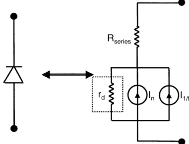
The basic current noise model of a diode, laser or otherwise, is shown in Fig. 2-4.
R
seriesr
In(ALI11/fFigure 2-4: One-port noise model of a diode.
The resistor Rseries is a parasitic resistance representing the losses in the Ohmic contacts of the diode. For the laser diodes measured for this thesis, this value is in the 2-10 Q range. Because it is a real resistance with actual power loss, it contributes noise as specified by the resistor noise model given above. In series are the parallel combination of the differential resistance rd, a 1/f noise source Il/f, and a current noise source I,.
The differential resistance rd is not a real resistance in the sense that it is capable of dissipating power, but is rather a ratio of the small change in voltage to the corresponding change in current across the junction; it is therefore depicted as ideal. The current through
36 CHAPTER 2. THEORY OF ELECTRICAL SYSTEM NOISE MODELING
a diode is typically approximated by an exponential law of the form
Vi
I = Is (e nkT - 1) (2.3)
where I is the current through the diode, I, is the saturation current of the diode, V is the voltage across the diode, q is the charge of an electron, k is Boltzmann's constant, T is the temperature of the diode, and n is an empirical fitting constant of order 1 which can have a weak bias dependence. The differential resistance is found as:
dV nkT nkT (2.4)
d- - Vq (
dI qIenk qI
For higher frequency modeling, one includes diffusion and depletion capacitance in parallel with Rd.
The precise origins of the Ii/f noise source are still poorly understood, but it typically takes the form:
SI,/f(f) = 0I C (2.5)
Typically 3 and -y are of order 1, and a varies widely depending on the diode. A helpful parameter is the 1/f noise corner frequency, which is the frequency at which the 1/f current noise power SI,i/f equals the noise current power Sin. This typically occurs at around 10 kHz, but can range between 1 kHz and 1 MHz.
The noise current source I1 in the diode model is taken to be an instance of a Gaussian stochastic process with white spectral density. This is a reasonable approximation in the low frequency limit in which one is interested in frequencies less than the inverse of the characteristic carrier scattering and transport times of the diode, as is the case in this thesis. The magnitude of this noise, or more precisely the noise power per unit frequency, is dependent on the detailed physics of the diode, and sometimes the bias current. For example, in a simple tunnel junction, each carrier's transport across the junction is largely
independent of the other carriers. This results in a current spectral density of: qV
SItj = 2qlDCcoth( k) (2.6)
2kT
Here IDC is the DC bias current through the diode, and V is the voltage across the junction of the diode. For most other types of diodes the situation is more complicated. Even in a simple p-n homojunction, which is known to (roughly) display shot noise behavior, the physics of what really goes on and where the noise comes from is quite subtle [28]
[29].
It is very common even in recent papers to attribute the noise in a forward biased semiconductor homojunction laser to the noise of two terminal currents in the laser, one in the forwardVq
direction of magnitude If = Ienkr and one in the reverse direction of magnitude I, Is.
With some fuzzy thinking, one could decide that the carriers in these currents cross the junction of the device in a independent manner, resulting in Poisson statistics and shot noise.
For low frequencies (compared to the transport times of the diode) this model happens to give the correct noise spectral density:
SI,hid = 2q(If + Ir) (2.7)
Unfortunately, this simple explanation, while appropriate for some devices (like a vacuum triode operated in the thermally-limited current regime), is simply wrong for a typical semiconductor diode. The noise model of the semiconductor diode is discussed more in Chapter 4, but it is sufficient to observe here that the carrier fluxes which actually cross the depletion layer of a diode are much larger than the currents measured at the terminals
[28], invalidating the 'independent transport' explanation. Unfortunately, this erroneous
explanation is still common in published work and textbooks on electronic devices.
In general, in trying to assess the noise added to a measurement from a diode, it is reasonable to assume a simple shot noise model SI, = 2qIDC as an order of magnitude estimate. But to take a Parthian shot at even this rough of a generalization, a heterojunction laser biased just above the threshold of lasing can display SI, at a thousand times the shot
38 CHAPTER 2. THEORY OF ELECTRICAL SYSTEM NOISE MODELING
noise level.
2.3
Two-port Equivalent Noise Models
2.3.1 Transistors
The most important part of most sensitive electronic measurements is the amplifier which boosts the signal to a level useful for data aquisition. To understand the noise in amplifiers, it is necessary to first understand the noise in their constituent transistors. The noise models presented for these devices will be in the common-emitter hybrid-pi model for bipolar junction transistors (BJTs), and the analogous common-source small signal model for field-effect transistors (FETs). While these models are very useful, like the diode model they should not be taken as gospel truth, but rather as good approximations which may differ from reality for different materials and geometries.
The noise model for a BJT is shown in Fig. 2-5. The resistance Tb is the base parasitic
b
rb/2 rb/2 rbcC
p
~
...A/LJ%...-'1/f 1b,sh be ce
9mvs Iec,sh
Figure 2-5: Two-port noise model of a bipolar junction transistor.
resistance and is engineered to be as small as possible, generally between 10 and 200 Ohms. The resistance rbc is the parasitic resistance between the base and the collector and is usually large enough to neglect. The two ideal resistances are Tbe and rce. They are the differential resistances of the forward biased base-emitter junction and the differential resistance of the reverse biased base-collector junction, respectively. b,sh is due to shot noise in the base
current and has the power spectral density
S, ,sh = 2qIB (2.8)
where IB is the DC current flowing into the base. Likewise Ic,sh is shot noise from the collector current with spectral density
Sl,c,sh = 2qIc (2.9)
where Ic is the DC collector current. Also shown in Fig. 2-5 is the 1/f noise generator
I/f accompanying the base current. As in the diode noise model, this noise has a spectral
density
SIi/f (f) DC (2.10)
This noise generator has been placed in the middle of the base resistance rb in an effort to accurately model empirical results
[30].
Finally, it must be remembered that the non-ideal resistances in the model carry noise according to the resistor noise model. Practically speaking, Tbc is large enough so as to render its noise sources unimportant, and the base resistance rb generally does not display significant 1/f noise.The noise model for a general FET device is shown in Fig. 2-6. For a typical FET,
Zgd
d
p
r0
40 CHAPTER 2. THEORY OF ELECTRICAL SYSTEM NOISE MODELING
R(z,,)
andR(zgd)
are very small, and the impedances can be taken to be pure capacitors. Physically speaking, the real parts of these impedances are vanishingly small because in modern processes the gate oxide in a MOS structure which insulates the gate from the other two terminals can be made with very few defects. At low frequencies, the only remaining impedance is the drain to source resistance, which is the effective resistance seen across the channel from the output of the transistor. The resistance is modelled as ideal even though it is dissipative and therefore contributes thermal noise. The thermal noise from the channel is added in separately later.I/f is the usual 1/f noise generator for the drain current with spectral density
SI,1/f (f )= (2.11)
Ith is related to the thermal noise of the channel, although its exact calculation is somewhat complicated, and involves an integral over the length of the channel [29] [28]. Below satu-ration, when the channel of the FET is not pinched off, the value of the spectral density is the usual thermal noise:
St ~ 4kTgm (2.12)
Above saturation, when the FET is pinched off (normal operating condition), the spectral density is different:
S1th ~ -4kTgmn (2.13)
3
The noise source I9 represents shot noise of the gate leakage current, and has the spectral density
Sl,g =- 2qIG (2.14)
where IG is the DC gate leakage current [29]. For most modern FETs, this leakage current is very small, and this noise source is unimportant compared to the thermal noise.
The noise models for BJTs and FETs described above are important for deciding what devices to use for a particular measurement.
2.3.2 Transformers
In the context of this thesis, transformers were used to impedance match noise sources with measuring amplifiers. Fig. 2-7 shows the noise model of a 1:N transformer with the '1' side chosen as the input. The resistances rp and r, are primary and secondary coil resistances,
... ... r
rCr
1 : N L 1I N C
Figure 2-7: Two-port noise model of a transformer.
respectively. They obey the usual resistor noise model; thermal noise from these devices typically dominates the noise from the transformer. The resistance rec represents magnetic core losses, and like any dissipative process, contributes thermal noise. The inductance LP is the primary inductance, which sets the low frequency limit of the transformer. The capacitance C, models the distributed parasitic capacitance of the secondary coil, and often sets the high frequency limit of the transformer.
2.4
Theory of One-ports and Two-ports
Because the noise generated in the circuit models given above is typically a small signal, the formalism of linear circuit theory can be applied to predict a system's noise behavior even when nonlinear elements are involved, as long as the system maintains a stable bias. This formalism allows one to abstract away from the particular circuit elements to generalized one-port and two-port devices. Some results of this theory which are central to this thesis are presented here.