This article presents a new integrated microfluidic/mi-crooptic device designed for basic biochemical analysis. The microfluidic network is wet-etched in a Borofloat 33 (Pyrex) glass wafer and sealed by means of a second wafer. Unlike other similar microfluidic systems, elements of the detection system are realized with the help of microfabrication techniques and directly deposited on both sides of the microchemical chip. The detection system is composed of the combination of refractive circular or elliptical microlens arrays and chromium aperture arrays. The microfluidic channels are 60 µm wide and 25 µm deep. The elliptical microlenses have a major axis of 400 µm and a minor axis of 350 µm. The circular microlens diameters range from 280 µm to 350
µm. The apertures deposited on the outer chip surfaces
are etched in a 3000-Å-thick chromium layer. The overall thickness of this microchemical system is <1.6 mm. A limit of detection of 3.3 nM for a Cy5 solution in phosphate buffer (pH 7.4) was demonstrated. The cross-talk signal measured between two adjacent microchannels with 1 mm pitch was <1:5600, meaning that e1.8 × 10-4% of the fluorescence light power emitted from one microchannel filled with a 50 µM Cy5 solution reaches the photodetector at the adjacent microchannel. This performance compares very well with that obtainable in microchemical chips using confocal fluorescence systems, taking differences in parameters, such as excitation power into microchannels, data acquisition rates, and signal filtering into account.
Following the introduction of the total analysis system concept (TAS) in 19831, miniaturized forms of TAS, called µTAS, began
to be investigated in the 1990s.2-5As shown in ref 2, miniaturizing
total analysis systems not only enables a size reduction of the analytical system, thus allowing portable systems and a significant reduction of reagent and sample consumption, but also improves TAS performance. Microfabrication techniques developed by the
semiconductor industry6,7 capable of realizing structures with
micrometer feature size, have been used by many groups to realize various types of miniaturized systems for chemical analysis in microfluidic channels8-10. The detection modes in these systems
can be as varied as UV-vis absorbance11-13, refractive index
measurements,14,15electrochemical detection,16,17or laser-induced
fluorescence detection (LIF)18-20. Because of its selectivity and
high sensitivity2,21,22, LIF continues to be the most preferred
detection technique for microchemical chips.
Like the system described in the work of Webster et al.,23in
which a photodiode was integrated onto a silicon substrate with a microfluidic system, the device presented here takes advantage of microfabrication technology to directly integrate the detection system onto the chemical analysis chip.24Unlike Webster et al.,
our detection system is integrated onto a Pyrex glass microfluidic chip. Since Pyrex is a very good electrical insulator, using high voltages inside the chip, for example, for capillary electrophoresis,
* E-mail: [email protected].
(1) Widmer, H. M. Trends Anal. Chem. 1983, 2, 77-79.
(2) Manz, A.; Graber, N.; Widmer, H. M. Sens. Actuators, B 1990, 1, 244-248. (3) Manz, A.; Harrison, D. J.; Verpoorte, E. M. J.; Fettinger, J. C.; Paulus, A.;
Ludi, H.; Widmer, H. M. J. Chromatogr. 1992, 593, 253-258.
(4) Harrison, D. J.; Fluri, K.; Seiler, K.; Fan, Z. H.; Effenhauser, C. S.; Manz, A.
Science1993, 261, 895-897.
(5) Jacobson, S. C.; Hergenro¨der, R.; Koutny, L. B.; Ramsey, J. M. Anal. Chem.
1994, 66, 1114-1118.
(6) Sze, S. M. Semiconductor Devices, Physics and Technology; John Wiley & Sons: New York, 1985.
(7) Kovacs, G. T. A. Micromachined Transducers Sourcebook; McGraw-Hill: New York, 1998.
(8) Jakeway, S. C.; de Mello, A. J.; Russell, E. L. Fresenius’ J. Anal. Chem. 2000,
366, 525-539.
(9) Manz, A.; Becker, H. Microsystem Technology in Chemistry and Life Sciences; Springer: Berlin, 1998.
(10) Bruin, G. J. M. Electrophoresis 2000, 21, 3931-3951.
(11) Verpoorte, E.; Manz, A.; Lu¨di, H.; Bruno, A. E.; Maystre, F.; Krattiger, B.; Widmer, H. M.; van der Schoot, B. H.; de Rooij, N. F. Sens. Actuators, B
1992, 6, 66-70.
(12) Liang, Z.; Chiem, N. H.; Ocvirk, G.; Tang, T.; Fluri, K.; Harrison, D. J. Anal.
Chem.1996, 68, 1040-1046.
(13) Salimi-Moosavi, H.; Jiang, Y.; Lester, L.; McKinnon, G.; Harrison, D. J.
Electrophoresis2000, 21, 1291-1299.
(14) Burggraf, N.; Krattiger, B.; de Mello, A. J.; de Rooij, N. F.; Manz, A. Analyst
1998, 123, 1443-1447.
Performance
of an Integrated Microoptical System for
Fluorescence
Detection in Microfluidic Systems
Jean-Christophe Roulet, Reinhard Vo1 lkel, Hans Peter Herzig, Elisabeth Verpoorte, Nico F. de Rooij, and Rene´ D1andliker
InstituteofMicrotechnology,UniversityofNeuchaˆtel,rueA.-L.Breguet2,CH-2000Neuchaˆtel,Switzerland
(15) Swinney, K.; Markov, D.; Bornhop, D. J. Anal. Chem. 2000, 72, 2690-2695.
(16) Rossier, J. S.; Roberts, M. A.; Ferrigno, R.; Girault, H. H. Anal. Chem. 1999,
71, 4294-4299.
(17) Martin, R. S.; Gawron, A. J.; Lunte, S. M. Anal. Chem. 2000, 72, 3196-3202.
(18) Ocvirk, G.; Tang, T.; Harrison, D. J. Analyst 1998, 123, 1429-1434. (19) Jiang, G.; Attiya, S.; Ocvirk, G.; Lee, W. E.; Harrison, D. J. Biosens.
Bioelectron. 2000, 14, 861-869.
(20) Chabinyc, M. L.; Chiu, D. T.; MacDonald, J. C.; Abraham, D. S.; Christian, J. F.; Karger, A. M.; Whitesides, G. M. Anal. Chem. 2001, 73, 4491-4498. (21) Fister, J. C., III; Jacobson, S. C.; Davis, L. M.; Ramsey, J. M. Anal. Chem.
1998, 70, 431-437.
(22) Haab, B. B.; Mathies, R. A. Anal. Chem. 1999, 71, 5137-5145. (23) Webster, J. R.; Burns, M. A.; Burke, D. T.; Mastrangelo, C. H. Anal. Chem.
2001, 73, 1622-1626.
(24) Roulet, J.-C.; Verpoorte, E.; Vo¨lkel, R.; Herzig, H. P.; de Rooij, N. F.; Da¨ndliker, R. J. Microelectromech. Syst. 2001, 10, 482-491.
1 Published in Analytical Chemistry, 74, issue 14, pp. 3400–3407, 2002,
is less critical than with Si substrates. Moreover, the chemical properties of Pyrex are well-understood and its high degree of chemical inertness continues to make it an attractive material for microfluidics. The interest here, then, was the development of an integrated microoptical/microfluidic platform that could ulti-mately be used for electrokinetically driven bioanalysis, such as that described in ref 25, realized for heterogeneous immunoassay. The detection system used here is made up of layers of microlens and chromium aperture arrays. This approach enables the fabrica-tion of small and closely spaced optical elements, their precise alignment with respect to the microfluidics, and the realization of original detection system configurations.26As shown in Figure 1,
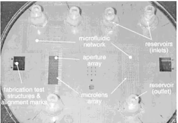
the chip is made up of a 0.5-mm-thick cover wafer and a 1-mm-thick wafer in which microfluidic networks are patterned by photolithographic techniques and etched in hydrofluoric acid (HF).27,28Both wafers are 100 mm in diameter. Two patterned
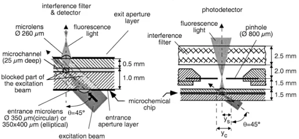
chromium layers and refractive microlenses, deposited directly on both sides of the chemical chip, form the detection system. The photoresist microlenses are fabricated by melting tech-niques.24,29Figure 2a presents the detection principle. As discussed
in ref 26, an off-axis illumination scheme can be used to improve the geometric separation between the excitation beam and the fluorescence light emitted from the microchannel. The incoming laser beam, forming a 45°angle with respect to the chip surface, is first focused into a 60-µm-wide, 25-µm-deep microchannel with the help of a first refractive microlens. For an excitation beam diameter larger than the excitation side microlens, the part of the beam that is not focused by the microlens (and, thus, unsuitable for dye excitation) is blocked by an aperture formed in a thin chromium layer. On the other side of the microchemical chip, a microlens collects and focuses the fluorescence light emitted from the microchannel onto a detector. The second exit aperture layer
prevents the unabsorbed excitation beam from being scattered onto the detector. The combination of geometric separation (off-axis illumination scheme) and spectral filtering with an interfer-ence filter placed after the collection microlens (Figure 2b) enabled detection performances comparable to those obtained with standard confocal systems. The first part of this article deals with the microfluidic/microoptic device layout and the measure-ment setup. The second part is devoted to the presentation of measurements carried out with Cy5 solution and the comparison of these results with those obtained with a comparable microfluidic device but with a confocal epifluorescence detection scheme.19
EXPERIMENTAL SECTION
Chip Design and Operation. Pyrex glass was chosen as the microchemical chip material since it is transparent in the visible range, chemically very inert, and electrically nonconductive, enabling electroosmotic pumping. As shown in Figure 3, the microfluidic network layout is T-shaped, with the holes allowing for the access to the microchannels placed at the end of each branch of the “T”. This layout was designed for simple electro-kinetic mixing experiments, with sample concentration monitoring after the T-junction. If one of the inlet reservoirs is filled with a buffer solution and the other one with a dye solution, the sample concentration after the T-junction is determined by the ratio of electroosmotic flows in each branch given by the potentials applied between the outlet and the inlets. The meander geometry between the inlets and the T-junction and between the T-junction and the detection area (division of the single microchannel into four parallel microchannels, numbered 1-4 from left to right) increases the overall length of the microchannels from one inlet to the outlet. The channel resistance is also increased with length and reduces the current for a given potential. The power dissipated in the microchannels in the form of heat is, thus, also reduced. The length from the inlet to the T-intersection is 45 mm. The total length from one of the inlets to the outlet is 89 mm for the inner detection area microchannels, 2 and 3, and 91 mm for the outer channels, 1 and 4, respectively. The microchannels are∼25 µm deep and∼60 µm wide. Two types of reservoirs were used during the work. The first type was made from sections of poly(vinyl chloride) (PVC) tubing glued onto the microchemical chip around the access holes using a two-component epoxy glue. Since the tube section was not always perfectly flat and in contact with the chip surface, it was thought that some solution might leak into the interstice, which would render complete rinsing of the reservoirs difficult. This is why a more advanced connector was designed. This one was formed by gluing a stainless steel nut onto the chip and screwing a polyethylene reservoir into it. Since it could be removed and even replaced by another type of reservoir if needed, the reservoir and the chip surface around the inlet/ outlet could be perfectly rinsed.
Though the chip was designed for electroosmotic flow, the lack of availability of a high voltage power supply at the time this study was carried out led to the use of a vacuum pump instead. Samples and cleaning solutions were introduced into the inlet reservoirs and pumped through the microfluidic channels to the outlet by means of a membrane pump connected to the outlet. The vacuum at the outlet was ∼320 mbar, and the flow rate, measured by monitoring the deionized (DI) water volume pumped
(25) Dodge, A.; Fluri, K.; Verpoorte, E.; de Rooij, N. F. Anal. Chem. 2001, 73, 3400-3409.
(26) Roulet, J.-C.; Verpoorte, E.; Vo¨lkel, R.; Herzig, H. P.; de Rooij, N. F.; Da¨ndliker, R. Opt. Eng. 2001, 40, 814-821.
(27) Fan, Z.; Harrison, D. J. Anal. Chem. 1994, 66, 177-184.
(28) Stjernstro¨m, M.; Roeraade, J. J. Micromech. Microeng. 1998, 8, 33-38. (29) Nussbaum, P.; Vo¨lkel, R.; Herzig, H. P.; Eisner, M.; Haselbeck, S. Pure Appl.
Opt.1997, 6, 1-20.
Figure 1. Topside view of the complete chip with two microfluidic
systems (fluorescence collected from this side). The left microchemi-cal system has all the optimicrochemi-cal element layers, whereas the right one has no aperture layer. The glued reservoirs where the sample/buffer solutions are introduced are also visible.
to establish itself mainly in the two inner microchannels. Since the path length is shorter for the inner microchannels, and hence, the flow resistance is slightly lower, the solution flowed prefer-entially into these channels. Sometimes, though, the flow switched from one inner microchannel to an outer microchannel. This was often due to dust particles perturbing the solution flow or clogging a microchannel. Generally speaking, inner channels were used in measurements.
Dye Preparation. The dye chosen here was a Cy5 cyanine fluorochrome (Amersham Life Science Ltd., Bucks, England), and all the samples used for fluorescence measurements were prepared from stock solution consisting of 50 µM Cy5 in a 50 mM phosphate buffer at pH 7.4. The 50 µM solution was obtained by dissolving 0.4 mg of Cy5-OSu monofunctional reactive dye in 10 mL of a pH 7.4 phosphate buffer solution. The buffer itself was prepared by mixing 19 mL of 100 mM NaH2PO4with 81 mL
of 100 mM Na2HPO4. The stock solution was kept in the dark at
∼6°C. Samples at lower concentration were prepared by dilution of the stock solution with phosphate buffer. Samples were always allowed to warm to ambient temperature before utilization.
Optical and Data Acquisition Setup. The experimental setup was composed of two parts, the excitation setup and the chip holder/collection setup. The excitation setup was made up of a 10 mW, 1135p HeNe laser (Uniphase Corp., San Jose, CA). The waist radius, w0, of this laser was 0.35 mm. To get the largest
excitation intensity in the microchannel, the polarization of the laser was turned parallel to the incident plane (TM polarization). To control the excitation intensity, an intensity controller consist-ing of a half-wave plate followed by a linear polarizer was placed at the laser output. By setting the polarizer parallel to the laser polarization and turning the half-wave plate, it was possible to control the excitation intensity while keeping the polarization orientation of the excitation beam constant (parallel to the incident plane). For ease of use, the excitation power was always measured after the intensity controller. The excitation power coupled into the microchannel and used for fluorochrome excitation is given by the power coupled into the chip by the excitation side microlens minus the interface losses (air-photoresist, photoresist-Pyrex,
Figure 2. Cross sectional view of (a) the detection system deposited onto a glass chemical chip and (b) the microchemical/microoptical chip
and the pinhole and interference filter.
Figure 3. Microchannellayoutofthechemicalchip.
through the system for over 2 h, was 42 ( 3 nL/s. All of the measurements with the microchemical chips were performed on the same setup and according to the same microchemical chip preparation protocol. One hour before beginning a series of measurements, the HeNe laser used as the excitation source was switched on in order to have a stable excitation power. At the same time, the microfluidic channels were thoroughly cleaned and conditioned for use. All solutions were loaded into the reservoirs using syringes equipped with 0.2-µm Millex-FG filters (Millipore SA, Bedford, MA). First, the reservoirs were rinsed three times with DI water. DI water was then drawn through the microchannels for 20 min. Then, the DI water in the reservoirs was replaced by a 0.1 M solution of NaOH (HPCE grade, Fluka Chemicals, Buchs, Switzerland; 0.2-µm-filtered prior to packaging). The NaOH solution was drawn for 10 min through the micro-channels. The NaOH solution was in turn replaced by DI water, which was pumped through the microchannels for 20 min. The microchemical chip was then ready to be used for the measure-ments.
Using a microscope, observation of the solution flow in the four parallel detection microchannels showed that the flow tended
and Pyrex-water). This may be estimated as follows. If the entrance pupil is defined by the excitation microlens rim, the optical power Pmcarried within a microlens is then given by
where I(F, z) is the optical intensity over a transverse plane perpendicular to the light propagation axis30 and F(φ) is the
distance from the center to the rim of the ellipse formed by the projection of the microlens onto a plane perpendicular to the excitation beam. F(φ) in eq 1 is a function of the microlens radius, rL, and the incident angle, θ. Assuming a Gaussian intensity
distribution,30P
mbecomes, after integration
where I0 and w0 are, for z ) 0, the intensity on the beam
propagation axis and the minimum value of the beam waist radius (in the plane perpendicular to the beam propagation), respectively. wzis the beam waist radius at the level of the excitation microlens. Equation 2 can be calculated numerically. According to the Fresnels equations30, the reflection losses, R
M, for a TM polarized
beam are
where n1and n2are the refractive indices on both sides of the
interface, and θ1 and θ2are the incident and refractive angles,
respectively. Thus, the excitation power coupled into the micro-chemical chip for an excitation microlens radius of 175 µm and for an incident angle of 45°was estimated to be 4.7% of the original beam power, with reflection losses of 1.5% for a polarization parallel to the incident plane. For example, the excitation power coupled into the chip for a 5 mW laser power after the intensity controller is 0.24 mW.
A measurement of the excitation power coupled into the chip was realized with a special chip for an incident angle of θ ) 0°. This chip had lens and aperture arrays deposited on the excitation side as shown in Figure 2, but consisted of a single, 1.5-mm-thick Pyrex glass wafer without the microfluidic network. The power was measured by placing the photodetector head on the collection side of the chip in place of the photodetector. The difference between the calculated excitation power and the measured one is <0.6%. The actual excitation power was measured experimen-tally with a Labmaster power meter (Coherent, Auburn, CA) equipped with an LM-2 detector based on a calibrated photodiode. The power meter precision was (5%.
The chip holder was mounted on an xy table so that the chip, and hence the microlens chosen for the excitation, can be precisely aligned with respect to the excitation beam. The detection system was composed of a second xy table, mounted
directly onto the chip holder, and a z-axis translation stage. Either a standard microscope fitted with a CCD camera or a photode-tector holder could be mounted on the z-axis translation stage. The microscope was used to observe excitation and fluorescence light distribution inside the chip, whereas the photodetector was used to make quantitative measurements. The CCD camera was a 6700-series CCD camera (Cohu Inc., San Diego, CA). The 04 TFF 002 microscope body (Melles Griot Inc., Irvine, CA) was equipped with a ×25 (0.25) microscope objective (Spindler & Hoyer, Go¨ttingen, Germany). Images on the collection side were also taken by the same CCD camera mounted on a type-S M3Z stereoscopic microscope (Leitz, Heerbrugg, Switzerland). The image acquisition and treatment were realized on a Macintosh computer with NihImager software (Scion Corp., Frederick, MD). The image acquisition setup was calibrated by means of a USAF-1951 resolving power target. The photodetector, an H5701-5 photomultiplier (Hamamatsu, Japan), was mounted in place of the standard microscope system to realize quantitative measurements. The photomultiplier holder was designed to hold an interference filter and a pinhole in front of the photomultiplier window, as shown in Figure 2b. The 670DF40 interference filter (Omega Optical Inc, Brattelboro) was specially designed for the Cy5 fluorochrome. The transmission was∼90% between 662 and 688 nm, with an attenuation >10-3% at 633 nm (excitation wavelength). The 800-µm-diameter pinhole was a precision 04 PPM-series mounted pinhole (Melles Griot Inc., Irvine, CA). According to the data sheet, the electronic bandwidth of the photomultiplier output signal is 20 kHz. The photomultiplier signal was processed by a PC equipped with a PCI-MIO-16E-4 data acquisition card and LabVIEW software (National Instruments Corp., Austin, TX). The sampling rate was 10 Hz (10 samples/s), and all data were smoothed using a 21-point-box smooth algorithm implemented in IgorPro (Wavemetrics, Lake Oswego). According to the Nyquist sampling theorem, a sampling rate of 10 Hz is insufficient to reproduce the temporal behavior of a signal having a bandwidth BPHof 20 kHz; however, our purpose was not to reproduce the
temporal behavior of the noise, but rather to average the noisy signal over a certain number, N, of samples. The integration time, T, of each sample is given by T ) 1/(2BPH). The effective
integration time of the averaging over N samples is, hence, NT, corresponding to an equivalent bandwidth of BN) 1/(2NT) )
BPH/N (if the sampling rate is slower than the bandwith of the
signal). In our case, then, BN) (20 × 103)/21 ) 950 Hz. Raytrace
simulations of the optical system were performed with Raytrace 6.2 (developed by N. Lindlein, University of Erlangen, Germany). RESULTS AND DISCUSSION
Excitation. The path and shape of the excitation beam through the microchemical chip is crucial to achieve a good separation between excitation and fluorescence light and, hence, to get a good SNR (signal-to-noise ratio). Therefore, the shape of the excitation spot inside the microchannel and on the collection side was observed and compared to that predicted by the raytrace simulations. Since direct observation of the microchannel was necessary, the microchemical chip used did not have collection side aperture and microlens arrays. Moreover, to make the outgoing excitation beam spot clearly visible on the collection side, the glass surface over the second microfluidic network was
(30) Saleh, B. E. A.; Malvin, C. T. Fundamentals of Photonics; John Wiley & Sons: New York, 1991.
Pm)
∫
φ)02π∫
F)0F I(F, z)F(φ) dφ dF (1) Pm) - I0w0 2{
π 2-∫
φ)0 π/2 exp[
-2rL 2 (1 - sin2θ) wz2(1 - sin2θ cos2φ)]
dφ}
(2) RM) ry2)(
n2cos θ1- n1cos θ2 n2cos θ1+ n1cos θ2)
2 (3) 4the measured and predicted spot shapes were similar to the measured spot size appearing larger (210× 420 µm) than the spot of the raytrace diagram (106× 290 µm). Hence, 2-D raytrace simulations can be very helpful in predicting spot position, size, and shape of the excitation beam as it passes through the device. It was of interest to quantitatively evaluate the background light generated by scattering of the excitation beam at the microchannel interfaces, and especially by the wet-etched surface of the microchannel. To do this, the signal intensity was recorded under the same conditions (same setup, excitation intensity, and detec-tion sensitivity) for two different chips, one having a microfluidic network, and the other one, not (dummy chip). The dummy chip was simply a single 1.5-mm-thick Pyrex glass wafer. The same detection system (microlens and aperture arrays on both sides of the chip) was fabricated on both systems. The microchemical chip with the microfluidic network was filled with DI water. A circular microlens was used to focus the excitation beam into both chips (but an elliptical one could also have been used). The 670DF40 interference filter was placed in front of the photode-tector. During the first 30 s, the signal was recorded with the HeNe laser switched on. For the next 30 s the HeNe laser was switched off (no excitation). When the laser was on, the difference between the average signal for the chip with and without the microfluidic network was <6%. The signal for the dummy chip was greater, which may be explained as follows: First, the back-reflection of part of the excitation beam at microchannel interfaces in the microfluidic chip would somewhat decrease the signal. Second, because of the absence of a microchannel, a displacement of the position of the excitation beam, yc, toward the collection
aperture could lead to an increase of the background light collection in the dummy chip. Since the reflection losses are, according to eq 3, <0.1%, the signal difference is mainly due to the modification of the position of the excitation beam. Raytrace simulations confirm that ycis 17 µm smaller for a system without microchannels than for a system with microchannels. In any case, with respect to the SNR, the excitation light scattered by the microchannel surface is negligible when compared to the excita-tion light that reaches the photodetector with and without the microchannels.
Figure 4. Images of the excitation beam spot for (left) a circular microlens and (right) an elliptical microlens. The angle of incidence was 45°.
The microchannel was filled with DI water.
roughened with fine-grained sandpaper. The microchannels were filled with DI water.
Figure 4a shows the CCD picture (image taken with a charge-coupled device camera) of the excitation spot at the level of the microchannel. More precisely, the observation plane (object plane) is situated at the interface of the two wafers. The microchannel side walls are clearly visible on both sides of the excitation beam spot. Except for two “tails” trailing from the spot along the y axis parallel with the microchannel, the spot shape and dimensions are in good agreement with the raytrace simulations. Thus, the spot measured on the CCD picture (Figure 4a) is 47 × 58 µm, whereas the spot given by the raytrace simulation is 40 × 59 µm. The tails come mainly from optical aberrations due to the off-axis illumination scheme. When the circular excitation microlens with 350-µm radius (Figure 4a) is replaced by a 350 × 400 µm elliptical lens (Figure 4b), the tails disappear.
As shown in Figure 2a,b, the distance between the center of the circular excitation microlens and the excitation beam spot in the microchannel, ys, and the distance between the circular
excitation microlens and the excitation spot at the collection side of the device, yc, are important to maximize the fluorescence light
collection by the collection microlens and to ensure an efficient blocking of the excitation beam by the chromium layer. CCD images comparable to those shown in Figure 4 were taken to determine yc and ys for incident angles ranging from 10° to 60°.
The difference between the lengths measured on the CCD pictures and the lengths predicted by the raytrace diagrams are within 30 µm and 40 µm at the level of the microchannel and on the collection side surface, respectively. The measurements are, thus, in good agreement with the raytrace simulations. CCD pictures (with an incident angle of 45°) were also used to determine the spot size of the excitation beam on the collection side. To enable visualization of the spot, the collection glass surface was depolished with fine-grain sandpaper. Unfortunately, because of the increased surface roughness and the fact that the picture was not taken in a darkened room, the exact shape of the spot was difficult to determine. The presence of the excitation beam reflection on the excitation side made the spot shape and size even more difficult to determine. However, in both cased,
Fluorescence Light Collection. The fluorescence signal was recorded in a chemical chip with the complete detection system (Figure 2) for Cy5 solution concentrations ranging from 0 to 50 µM. The signal was first recorded for the full concentration range with the same circular excitation microlens, then the measure-ments were repeated with an elliptical microlens. The same stock solution of each dye concentration was used for both series of measurements. The recording procedure was the same for all measurements. Figure 5 shows the signal obtained for DI water and a 10 nM Cy5 solution (excitation power of 0.24 ( 0.02 mW). For the Cy5 solution, the signal was recorded for 50 s with the pump switched on, then for another 50 s with the pump switched off. The average signal was calculated from 300 data points between 10 and 40 s for when the pump was on and between 70 and 100 s for when the pump was off. The data for the pump switched off were taken after 70 s, because the signal required 10-20 s to stabilize. For the DI water, the procedure was the same, except that the excitation laser was switched off after 90 s to get an idea of the background level due to the remaining excitation beam reaching the photodetector. The average signal for DI water with no pumping was calculated from 200 points between 70 and 90 s. The detection volume can be evaluated as being the intersection of a cylinder of radius r (r being the average radius of the excitation spot between the two wafers) with a perpendicular half-cylinder having a 30-µm (microchannel) radius. The detection volume is 60 ( 10 pL for the circular excitation microlens (not taking into account the tails or aberrations seen in Figure 4a) and 66 ( 11 pL for the elliptical microlens.
The absolute values of the average signal obtained with the elliptical excitation microlens for dye solution (ShE) and for buffer solution (ShBE) were greater than the signals obtained with the circular microlens (ShCand ShBC). On average, ShEwas 15% greater than ShC, whereas for the buffer solution, ShBEwas 9% greater than ShBC. Since the base area of the elliptical excitation microlens is
13% greater than the circular excitation microlens, the excitation power coupled into the microchannel is∼13% greater, and hence, a signal difference of this magnitude was expected. However, as shown by the shapes of the two excitation spots inside the microchannel (Figure 4), the elliptical microlens has smaller aberrations for off-axis excitation and therefore gives a better focused spot. This leads to a more condensed excitation spot in
the microchannel and on the collection side. The excitation beam is, thus, more effectively blocked by the collection aperture layer, and hence, the amount of collected excitation light is less. This is why the signal intensity increase (ShBE- ShBC) obtained for the
microchannel filled with buffer solution is lower than expected from the difference in microlens base areas. Similarly, a better-shaped excitation spot in the microchannel explains why, for the microchannel filled with Cy5 solution, the signal intensity increase (ShE - ShC) is slightly larger than predicted by the microlens
difference in base area (15%). The probe volume is imaged at the pinhole position (Figure 2b), and the pinhole size (800 µm) was chosen to fit more or less the image of the probe volume produced by the elliptical microlens. Therefore, more fluorescent light was blocked in the case of the circular microlens (elongated excitation spot) than for the elliptical microlens (circular spot). Therefore, the elliptical microlens, besides enabling the coupling of a slightly larger excitation intensity into the microchemical chip, improves slightly the signal difference for microchannels filled with Cy5 solution versus buffer solution and, hence, improves the SNR. The results presented from now on were obtained with elliptical excitation microlenses.
Sensitivity. The average photodetector signal was measured for Cy5 solution concentrations ranging from 1 nM to 50 µM and proved to be linearly dependent on concentration over the full range. The slope of the curve was R ) 174× 103VM-1. The
average background signal was obtained when the microchannels were filled with buffer solution only (ShBE). The detection floor was
defined as a signal that is three times the total noise, σN, above
the background signal. The total noise for a background-corrected signal is calculated as the sum of the variances σE2and σBE2 of the fluorescence ShE and the background ShBE, respectively, which
means
The detection floor was calculated using measurements for a 1 nM concentration. Since σN) 188 × 10-6V and ShBE) 2.3 × 10⁻³
V, the limit of detection (LOD) of the system calculated from the intersection of the linear response curve (R ) 174× 103V M-1)
with the detection floor is LOD ) 3.3 nM.
The SNR (power of the background-corrected signal/noise power) is given by the relation
or
SNR is defined in eqs 5 and 6 in terms of electrical power rather than optical power. Optical power is determined directly by photon flux at the detector, which gives rise to an electrical current, i. SNR is then signal/σNand the LOD ) 3σN. Since electrical power
is proportional to i2, the SNR calculated for the electrical signals
Figure 5. Photodetector signal for a 10 nM Cy5 solution and DI
water. The data have been smoothed using a 21-point-box smooth algorithm. σN)
x
σE 2 + σ BE 2 (4) SNR )(ShE- ShBE) 2 σE 2+ σ BE 2 (5) SNRdB) 10 log (ShE- ShBE) 2 σE2+ σBE2 (6) 6that make up the detector output is the square of that calculated with optical power.31Seen in terms of electrical power, the LOD
becomes 9σN2. Using electrical power instead of optical power to calculate SNR is simpler, since it is easier to convert the signal and shot noise into electrical terms than to convert load resistor Johnson noise, multiplication noise, and so on into optical terms. Moreover, since measurement equipment is operated in volts and amperes, it is unnecessary to extract square roots in order to have good comparisons between different measurements.
The SNR of the 1 nM Cy5 signal is 4.3 or 6.4 dB. As noted by Mathies et al.,32the SNR should increase as the excitation power
increases until an optimum is reached. Then, as a result of ground-state depletion and photobleaching, the SNR will decrease. The power density giving the optimum SNR for a 10 nM Cy5 solution was determined by Jiang et. al19to be∼540 W cm-2for a flow
rate of 3.8 µL min-1. (In ref 19, the SNR was defined by the
background-corrected fluorescence signal divided by the standard deviation which, since it is optical powers, gives a SNR equivalent to the square root of the SNR defined in eq 5.) The SNRdBobtained
as a function of the excitation power for 10 µM and 10 nM Cy5 solutions was also measured in this study. The excitation power ranged from 0.05 mW to 0.42 mW, corresponding to a power density range of 5 W cm-2 to 44 W cm-2. The fluorescence
measured for both samples is proportional to the excitation power and the SNRdBranges from 15 (at 0.05 mW) to 25 (at 0.42 mW),
and from 49 (at 0.05 mW) to 55 (at 0.42 mW) for the 10 nM and 10 µM solutions, respectively. Hence, even if the flow rate in our chip was ∼6 times smaller, the maximum excitation intensity before bleaching had not yet been reached.
Since ShE, ShBE, and σN
2 (assuming shot noise limitation) are proportional to the excitation power, the SNR for an excitation power P2) kP1compared with the SNR for P1is given by
Thus, for k ) 0.42 mW/0.05 mW ) 8.4, the ratio of the maximum and minimum power measured previously, the SNR should increase by a factor of 8.4 or 9.2 dB. This result was confirmed for the 10 nM solution by the measured 10 dB difference of the SNR. For the 10 µM however, the measured SNRdB difference
over the range of power used was only about 6 dB. The SNRdB
difference between the 10 µM and 10 nM was∼34 dB. Since the fluorescence signal ShE (and hence, σE
2, assuming shot noise limitation) is proportional to the fluorochrome concentration for increasing fluorescence signal, the total noise σN
2 will be domi-nated by σE2(eq 4). Therefore, the SNR should increase propor-tionally with the concentration. This behavior was confirmed by the 30 dB increase in SNR for the concentration increase from 10 nM to 10 µM discussed above.
Results for a comparable microchemical chip, but with a confocal epifluorescence detection scheme, were reported by Jiang et al.19 With the same interference filter as we used here and
before optimization of the excitation source and the collection
system parameters, they reached a LOD of 1.5 nM for Cy5. As excitation source, they used a 11.5 mW laser diode at λ ) 634.5 nm. The photodetector signal was filtered using a 25 Hz low-pass filter, and the A/D sampling rate was 50 Hz. The digital signal was smoothed by means of a 21-point-box smooth. Table 1 gives a comparison of our detection system and the epifluorescence system reported in.19The upper section of Table 1 summarizes
the characteristics of the systems. The lower section of Table 1 gives a comparison of the LODs reached for the two systems as raw data and in terms of LOD normalized for bandwidth and for bandwidth and excitation power (in the microchannel). The LOD for equal bandwidth enables the direct comparison of systems with different signal filtering and, hence, with different bandwidths. Similarly, the LOD for equal bandwith and excitation power enables the comparison of systems with different bandwidths and excitation power. This comparison shows that the integrated system presented here is 10-20 times more sensitive. The better performance of the off-axis illumination scheme compared to the epifluorescence detection scheme is due to a better suppression of noise due to background light. In the epifluorescence scheme, ∼4% of the excitation power (eq 3) is reflected back from the surface of the microchemical chip. Part of this light is then collected by the microscope objective, which increases the background signal. This is not the case for the off-axis system, since the fluorescence light collection is not performed on the same side of the chip as the illumination. With a more selective interference filter and further optimization of excitation source and collection parameters, Jiang et. al19reached an ultimate LOD
of 9 pM for Cy5. Similarly, the LOD obtained with the integrated system presented in this paper could be improved by considering these types of parameters.
Cross-Talk. The amount of fluorescence and scattered excita-tion light emitted from a microchannel and collected by the collection optics at an adjacent microchannel was determined. The first measurement was performed by exciting the fluorescent dye
(31) Hobbs, P. C. D. Building Electrooptical Systems; John Wiley & Sons: New York, 2000.
(32) Mathies, R. A.; Peck, K. Anal. Chem. 1990, 62, 1-6.
Table 1. Comparison of System Parameters and Limits of Detection.
Jiang et al. system of this work power density (in microchannel) 1000 W cm-2 8.5 W cm-2 a spot size (diameter) 18 µm 60 µm excitation power (in microchannel) 2.6 mW 0.24 mW analogue signal filtering low-pass filter cutoff 25 Hz photomultiplier output bandwidth of 20 kHz sampling rate 50 Hz 10 Hz
data smoothing 21-pt box 21-pt box equivalent bandwidth 2.3 Hzb 950 Hzc LODc(SNR ) 9) 1.5 nM 3.3 nM LOD @1 Hzd 1.0 nM/xHz 0.1 nM/xHz LOD @1 Hz and 1 mWe 1.6 nMxmW/xHz 0.05 nMxmW/xHz
aCalculated for an excitation power of 0.24 mW and a spot radius
of 60 µm.bSince the sampling frequency is two times the
low-pass-filter cutoff frequency, the equivalent bandwidth, BN, after smoothing
over N points is BN) 2BF/(N + 1). BFis the signal bandwidth of the
signal after the low-pass filter.19 cThe equivalent bandwidth, B N,for
an average of N points is BN) BPH/N, where BPHis the bandwidth of
the detector. A 670DF40 Omega interference filter was used in both systems.dLOD normalized for bandwidth.eLOD normalized for
bandwidth and for the same excitation power.
SNR(P2) ) (kShE(P1) - kShBE(P1)) 2 k(σE 2 (P1) + σBE 2 (P1)) ) kSNR(P1) (7)
V, respectively). Hence, the measured fluorescence light is from microchannel 1 and not from the Cy5 solution in microchannel 2 excited by scattered light from microchannel 1. Comparing with the reference signal for 10 nM Cy5 the sensitivity, for channels 1 mm apart, would be limited to ∼10 nM for a 50 µM Cy5 solution concentration in the adjacent microchannels. The cross-talk CT is
given by the photodetector signal intensity Shc, measured in the
same microchannel as the excitation divided by the signal intensity Sha measured in an adjacent microchannel. Since Shc and Sha are,
for a 50 µM Cy5 solution, 10 × 103 V and 1.8 V, respectively, CT
) 10 × 103/1.8 = 5′600 (Sh
c was corrected to take into account
the different gain setting of the photodetector used when measur-ing Sha). CT could be further reduced by increasing the distance
between microchannels or by placing the collection microlenses in staggered rows instead of a single row to preserve the 1 pitch between channels.
CONCLUSION
We have successfully demonstrated the detection of a 3.3 nM solution of Cy5 fluorescent molecules in a microchemical chip combining microfluidic networks and microoptical elements. The cross-talk signal measured between two adjacent microchannels at 1-mm distance is 1:5600, which means that <∼1.8 × 10⁻⁴% of
the fluorescence light power emitted from one microchannel reaches the photodetector at the adjacent microchannel. We believe that with improved electronic signal processing and a further optimization of the detection system, a limit of detection in the range of 100 pM could be possible. Further improvement of the detection system could be accomplished, for instance, by increasing the microlens diameters, which would enable more efficient coupling of excitation power into the microchannels and collection of fluorescence. The 100 pM limit of detection could be lowered even further by using techniques in which sample is concentrated onto a surface25 or by field-amplified stacking in solution.33
A complete microchemical system with a large number of microchannels for simultaneous analysis of a large number of samples becomes possible as a result of the size and fabrication method of the microlenses and the possibility to deposit them directly onto a microchemical chip. This concept is highly adaptable, and with the integration of excitation light sources (laser diodes, VCSELs) and detectors (photodiodes or photo-multiplier arrays), a truly miniaturized µTAS could become a reality in the not-too-distant future.
ACKNOWLEDGMENT
The authors are thankful to Karl Fluri for his work on the microfluidic system and to Novartis Pharma AG. The project was funded by the Swiss priority program “Micro- and Nanosystems Technology” (MINAST).
(33) Lichtenberg, J.; Verpoorte, E.; de Rooij, N. F. Electrophoresis 2001, 22, 258-271.
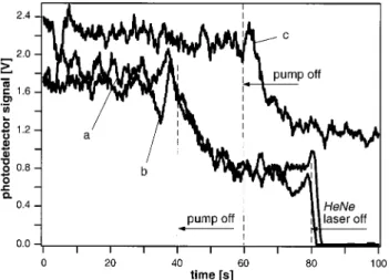
Figure 6. Signalmeasured(a)with50 µM Cy5solutionineach
microchannel,(b)withDIwaterinmicrochannel2,and(c)witha10 nMCy5solutionineachmicrochannel(collectionandexcitationon thesamemicrochannel).Theexcitationpowerwas0.24 ( 0.02mW.
in microchannel 1 (Figure 3) and measuring the signal intensity in the collection optics of microchannel 2 (cross-talk). To obtain the highest possible fluorescence signal (and, hence, the highest cross-talk signal intensity), a 50 µM solution of Cy5 was introduced into the microchannels. The second measurement was performed in a similar manner, but with microchannel 2 filled with DI water. This particular measurement was made possible, because micro-channel 2 happened to become clogged during rinsing of the chip with DI water. However, this channel could also have been filled with water by clogging it using UV-curable glue introduced via a hole drilled in the cover plate. The two cross-talk signals are designated in Figure 6 by the letters a and b. Finally, the cross-talk signals were compared with a reference signal obtained using fluorescent dye excitation and fluorescence light collection from the same microchannel, namely microchannel 2 (Figure 3). A 10 nM solution of Cy5 was drawn through the microchannels in that case. The reference signal is designated in Figure 6 by the letter c.
As shown in Figure 6, the cross-talk signals were recorded for 40 s with the pump switched on, after which the pump was switched off. After 80 s, the HeNe laser was also switched off. The reference signal (excitation and collection from the same microchannel) was recorded for 60 s with the pump switched on, with subsequent measurements made with the pump switched off.
Since both cross-talk signals decrease when the pump is switched off (indicative of photobleaching), it can be concluded that the cross-talk is mainly due to fluorescence light, rather than scattered excitation light. Moreover, the cross-talk signals are
about the same whether microchannel 2 is filled with Cy5 solution (a) or filled with DI water (b) (the average signal is 1.8 V and 1.7