A Data Processing Subsystem for the Holo-Chidi
Video Concentrator Card
by
Aditya Prabhakar
S.B. Electrical Engineering and Computer Science
Massachusetts Institute of Technology, 2000
Submitted to the Department of Electrical Engineering and Computer Science in Partial Fulfillment of the Requirements for the Degree of
Master of Engineering in Electrical Engineering and Computer Science
at the
Massachusetts Institute of Technology
August 30, 2001
© 2001 Massachusetts Institute of Technology
All rights reserved
Signature of Author...
Department of Electri Engineering and
ARCHIVeS
MASSACHUSETTS INSTITUTE OF TECHNOLOGYJUL 3 1 2002
LIBRARIES Computer Science August30, 2001 Certified by... V Stephen A. BentonE. Rudge and Nancy Allen Professor of Media Arts and Sciences
Thesis Supervisor
Accepted by... ...
Arthur C. Smith Chairman, Department Committee on Graduate Theses Department of Electrical Engineering and Computer Science
A Data Processing Subsystem for the Holo-Chidi
Video Concentrator Card
by
Aditya Prabhakar
Submitted to the
Department of Electrical Engineering and Computer Science Aug. 30t, 2001
In Partial Fulfillment of the Requirements for the Degree of Master of Engineering in Electrical Engineering and Computer Science
Abstract
A specialized board was designed to improve the performance of the Mark-II
Holographic Video system. Acting as a high speed-frame buffer, the Video Concentrator Card takes in a computed holographic frame, stores it in Video RAM, and formats and sends the data out to the display in analog form. In conjunction with the Avid Jupiter HD card, the two sets of cards would make up Holo-Chidi. Holo-Chidi is designed to be a stable and efficient method for delivering computed holographic fringes to the Holovideo system in real-time. A data processing system, the Data Handler, was developed to handle all the control signals on the board. Using programmable logic, the basic framework on the Data Handler was developed. Initialization processes were developed, as well as access process for the various components on the board.
This research was funded by the Digital Life Consortium at the MIT Media Laboratory.
Thesis Supervisor: Dr. Stephen A. Benton,
Title: E. Rudge and Nancy Allen Professor of Media Arts and Sciences, MIT Media Laboratory Project Supervisor: Dr. Thomas A. Nwodoh
Acknowledgements
This thesis would not have been possible without the support, guidance, and assistance of many people.
First, I would like to thank Prof. Stephen Benton for giving me the opportunity to work on such a challenging project such as Holo-Chidi. His holography class opened up a whole new and exciting field, which I had never known to exist. Through his support, I was able to do my part in contributing to the field of holography, by working on the Holographic Video system.
Dr. Thomas Nwodoh also deserves my thanks for allowing me to work on the Holo-Chidi project. Through his guidance and assistance, I was able to develop my skills as a
hardware designer from all aspects. Without his help, this project would not have been possible. I appreciate the patience he had with me, as I struggled to find solutions to the many problems in the Data Handler design. I also must thank him sincerely for being the chief editor for this document, making sure I had all my facts about the design correct.
Elroy Pearson, my fellow thesis survivor and officemate, provided me with no end of entertainment and support. He was always willing to listen to me babble on about finite state machines and timing diagrams. Elroy's assistance was invaluable in helping me formulate my design ideas, and also in helping me keep my sanity. I know this thesis would not have been possible if Elroy had not been there to help me whenever I needed it.
To the rest of the Spatial Imaging group, I want to thank them for their extensive knowledge and wisdom. I have learned a great deal about the field of holography from them. They lent their ears to a stressed graduate student, and provided me a supportive network of friends.
To my fellow M. Engers, Ashwinder Ahuluwalia, Jason Sharma, and John Paul Strachan,
I express my gratitude for keeping me entertained, as I struggled to complete my work.
Their camaraderie, whether it be from late night foosball escapades, or stiff video game competitions, helped to boost my confidence, even in the worst days of my research. A special thanks goes to Ash and Jason for keeping a roof over my head in my last week here at MIT.
To all of my old roommates, Spencer Liang, Danny Lai, and Bhuwan Singh, I do not believe I have met a nicer group of people. Your friendship through the years has helped me achieve my goals, and then some. Thank you for putting up with me, just like all brothers do. I want to add that this thesis would never have been printed were it not for the help of Mr. Singh.
To all my Boston B-boys and girls out there, I want to thank you for keeping me in shape, after hours of sitting in front of my computer. I will return.
To my sister, Pavitra Prabhakar, words cannot express how much her support has meant to me over the years. I would never have been able to accomplish all that I have, without her guidance and support.
To my parents, Padmini and R. Prabhakar, deserve more gratitude than I can ever give. They gave me the unconditional support I needed to survive all that I have been through at this school. Nothing I have ever accomplished could have been achieved without them. Through their belief in me and what I could achieve, I have become the man that I am today. Thank you from the bottom of my heart.
I could not have completed the work of this thesis without the support of these people,
and many others, who I may have forgotten to mention. I am in your debt. Thank you for making my time at MIT an experience I will never forget.
Table of Contents
CH A PTER 1: PU R PO SE ... 9
CHAPTER 2: HOLOGRAPHIC VIDEO...11
2.1 BACKGROUND ... 12
2.1.1 Holographic Video Display... 12
2.1.2 Cheops...12
2.2 CURRENT SYSTEM ... 14
2.2.1 M ark-II Holographic Video Display ... 15
2.2.2 Holo-Chidi...16
2.2.2.1 Avid Jupiter HD Processor Board ... 17
2.2.2.2 Video Concentrator Card... 18
CHAPTER 3: VIDEO CONCENTRATOR CARD...21
3.1 OVERVIEW ... 21
3.1.1 Improvements upon Cheops ... 22
3.1.2 General Design... 23
3.1.2.1 Cadence Design Software... 24
3.2 HARDW ARE FUNCTIONAL BLOCKS... 24
3.2.1 MPC850 Integrated Communications Microprocessor ... 24
3.2.2 Field Programmable Gate Array ... 26
3.2.3 LVDS Interface... 27
3.2.4 D igital to Analog Converter... 28
3.2.5 SDRAM ... 28 3.2.5.1 M ain M emory ... 29 3.2.5.2 Video M emory... 29 3.2.6 Flash ROM ... 30 3.2.7 Alphanumeric Display... 30 3.3 IM PLEMENTATION ... 31
CHAPTER 4: SYSTEM CONTROL LOGIC...33
4.1 G ENE RA FPG A OVERVIEW ... 33
4.2 A LTERA A PEX 20K 200E D ESIGN... 34
4.2.1 Overview... 34
4.2.2 Logic Elements... 36
4.2.3 Embedded System Block... 37
4.2.4 FastTrack Interconnect ... 38 4.3 SOFTW ARE ... 39 4.3.1 VHDL ... 40 4.3.2 Quartus II ... 41 4.4 D ESIGN PROCESS ... 41 4.4.1 Design Entry ... 42
4.4.2 Compilation and Functional Simulation ... 42
4.4.3 Logic Synthesis... 42
4.4.4 Place and Route... 43
4.4.5 Timing Analysis ... 43
CHAPTER 5: DATA HANDLER SYSTEM IMPLEMENTATION...45
5.1 G ENERAL D ESIGN ... 45
5.1.1 Top-level D esign... 45
5.1.2 Common D esigns... 47
5.1.2.1 Finite State M achine ... 47
5.1.2.2 Counters... 49 5.1.2.3 Bidirectional Signals... 50 5.1.2.4 Flip-flops ... 51 5.1.2 System D ebugging ... 51 5.2 SYSTEM INITIALIZATION ... 52 5.2.1 Design Overview ... 52 5.2.2 Timing Analysis... 53
5.3 ALPHANUMERIC DISPLAY PORT PROGRAMMING ... 54
5.3.1 Design Overview ... 54
5.3.2 Timing Analysis... 58
5.4 PROCESSOR Bus CONTROL ... 58
5.4.1 Design Overview ... 58 5.4.2 Timing Analysis... 60 5.5 FLASH RO M IMPLEMENTATION...60 5.5.1 Data Retrieval ... 60 5.5.1.1 Design Overview ... 61 5.5.1.2 Timing Analysis ... 62 5.5.2 Creating a ROM ... 63 5.6 SD RA M CO m OL...63 5.6.1 SDRAM Initialization ... 63. 5.6.1.1 Design Overview ... 63 5.6.1.2 Timing Analysis ... 66 5.6.2 SDRAM W rite ... 66 5.6.2.1 Design Overview ... 66 5.6.2.2 Timing Analysis ... 68
5.7 CURRENT SYSTEM STATUS...69
CHAPTER 6: CONCLUSION... 71
6.1 FUTUREW ORK ... ... .. . ... ... 71
APPENDIX A: MPC850 BUS ARBITER SIGNALS...73
Figures
FIGURE 1: OVERVIEW OF A HOLOVIDEO SYSTEM' ... 11
FIGURE 2: CHEOPS SYSTEM ARCHITECTURE3 . . . .13
FIGURE 3: OVERVIEW OF THE MARK-II HOLOVIDEO DISPLAY2... 15
FIGURE 4: BASIC LAYOUT OF THE HOLO-CHIDI SYSTEM... 17
FIGURE 5: GENERAL BLOCK DIAGRAM FOR VIDEO CONCENTRATOR CARD... 22
FIGURE 6: BLOCK DIAGRAM OF THE MPC8509... . . . .. . . 25
FIGURE 7: LVDS RECEIVER BLOCK DIAGRAM" ... 27
FIGURE 8: ALPHANUMERIC DISPLAY BLOCK DIAGRAM15 ... 30
FIGURE 9: APEX 20K200E DEVICE BLOCK DIAGRAM10 . . . . . . .. 35
FIGURE 10: APEX 20K200E LOGIC ELEMENT'0. . . . . . . . . . . . . . . . . . . . .36
FIGURE 11: APEX 20K200E ESB IN INPUT/OUTPUT CLOCK MODE'0 . . . .38
FIGURE 12: APEX 20K200E FASTROW INTERCONNECT'0 ... . . . ..39
FIGURE 13: FPGA DESIGN FLOW ... 41
FIGURE 14: GENERAL STRUCTURE OF THE DATA HANDLER SYSTEM... 46
FIGURE 15: GENERAL DESIGN FOR MOORE MACHINE FSM... 48
FIGURE 16: STATE DIAGRAM FOR SYSTEM INITIALIZATION ... 52
FIGURE 17: STATE DIAGRAM FOR ALPHANUMERIC DISPLAY PORT PROGRAMMING ... 56
FIGURE 18: STATE DIAGRAM FOR BUS CONTROL MODULE ... 59
FIGURE 19: STATE DIAGRAM FOR ROM DATA READ MODULE ... 61
FIGURE 20: STATE DIAGRAM FOR SDRAM INITIALIZATION ... 64
FIGURE 21: STATE DIAGRAM FOR SDRAM WRITE MODULE ... 67
Tables TABLE 1: APEX 20K200E DEVICE FEATURES '0 ... . . . .. . . 35
TABLE 2: MAPPING OF DATA, ALPHANUMERIC DISPLAY DATA, AND HEXIDECIMAL VALUES15 ... ... ... 54
TABLE 3: COMMANDS AND CONTROL SIGNALS FOR THE VCC SDRAM'... . . . . 65
Chapter 1: Purpose
This Master's Thesis focuses on the issues related to the design, implementation, and verification of a data-managing system, or Data Handler (DH). DH is the control system for the Video Concentrator Card (VCC). It manages the control logic and controls all the 1/0 chips on the board. The VCC acts in a similar fashion to a frame buffer contained in all video cards for the modem PC. The purpose of this design is to ensure that high bandwidths of data generated from multiple processor cards are
transmitted to the VCC, formatted, buffered, and then passed properly to the outputs. All these design points must occur as efficiently as possible, avoiding any timing issues, such as data contention and in conformity with valid setup and hold times (tsu and thold
respectively). Together, these design points and efficiency considerations create a very vast and complex system. While many commercial frame buffer cards exist in today's market, none can handle the magnitude of the bandwidth or processing power for the target system of this design: holographic video (Holovideo).
The material contained in this thesis is divided into 4 main chapters. The first chapter describes the holovideo system and how the VCC fits into that system. This section describes the predecessor system to VCC, or CHEOPS. The main focus of the second chapter is the general design of the VCC, with a look into the key components design of this system. The third chapter describes techniques for designing and
developing a control logic system: the materials with which to create one, the
methodology behind complex logical systems, in depth descriptions of the language used to create DH, and the chip on which the design will fit. Finally, the focus shifts to the actual development of DH. Its main modules are discussed in full, from design to implementation to verification.
The magnitude of this project is fairly vast. During the initial design stages, the schematics and layout notes were created, and a netlist was generated. Then the project shifted to acquisition of all the components that are contained in VCC. The components and designs were then sent out to an independent contractor for layout, fabrication, and assembly. Upon its return, the simulated designs of DH were tested in the actual board. This field-testing of DH created a greater understanding on how to create a "safe" design,
that while efficient, contains enough redundancy to eliminate possible errors that improper control logic can create.
The main scope of this thesis is to describe how to create modules for a data-management system. It gives a description of the requirements of the system, how to implement the system, and the actual design of that system. The system itself is divided into seven main modules, some containing several sub-components. The interaction of these modules is essential for the creation of a functioning system, while allowing it to be
as easy as possible for future designers to understand. The thesis concludes with some potential research areas that can be pursed using the components outlined in this thesis.
Chapter 2: Holographic Video
Holographic video is an electronic imaging system that can render and display computer generated holograms at near-video rates. Holographic video was developed by Dr. Stephen A. Benton et. al. at the MIT Media Lab in the late 1980's.' The Mark-II Holovideo display is the current generation of that initial work.
Overview of a Holovideo System
3-D Image
Ik
Viewer Fringe Display Computation System. User Interface, Content processingFigure 1: Overview of a Holovideo System'
Dr. Benton's group developed the Mark-Il system in the early 1990's.2 The system is capable of producing 36-MB images as large as about 150 mm in width, 75 mm in height, and 100 mm depth. The computation involves transforming a 3-D numerical description of the object scene into a holographic fringe pattern.
Unfortunately, many of the possible avenues of research for this system have yet to be explored, due to the fact that the computational tools, modulation tools and the communication bandwidth are limited. Imagine having a holographic television in your home, or a cardiologist having the ability to look at a moving holographic representation of a patient's heart to "see" if any problem areas exist. These potentials cannot be accessed by the system that currently exists. The main bottleneck for this system is the computation hardware that is connected to the Content Processing, between the user interface and the fringe computation. To tap the potential of holovideo, its hardware needs to be upgraded beyond its current specifications, to allow for faster computation and rendering.
2.1
Background
2.1.1 Holographic Video Display
The initial work on electronic holography began in 1987 at the MIT Media Lab. It was not until 1989, before the researchers were able to display simple geometric patterns on the holographic display. At that time, only horizontal scan lines of low spatial resolution were available for the display. This system only supported a single channel, on which 2MB of data could be transmitted. By 1990, an increase in the number of scan lines allowed a higher resolution hologram to be displayed, while three channels of data could be supported. The following year, further progress was made, as the display could support color images. In 1992, additional channels were added to the display. It could now display 36 MB of data, transmitted through 18 channels, or holo-lines, as they were called. This became available through the use of a new image processing system, known as Cheops. Cheops had a large reconfigurable frame buffer and also contained hardware for computing holographic data. Using this large amount of data, the viewing size and image volume of the display were greatly increased, creating a convincing 3-D image. 3 This version is the current model being used for research at the
MIT Media Lab.
2.1.2 Cheops
The hardware that supplies the appropriate data to the holographic display is known as Cheops. Cheops was developed by the Information and Entertainment group at the MIT Media Lab in 1995. The Cheops Imaging System is a compact, modular
platform for acquiring, processing, and displaying video sequences and model-based representations of moving scenes. This hardware allowed the user to perform several
different operations on streaming data, a task, when left to software, is incredibly computationally intensive. It has the ability to perform these tasks in parallel by using
dynamic scheduling of resources. It also contains buffers that enable slower-than-real-time processing of data, when the demand for data exceeds the resources available. This quality made it an ideal choice for use with the Holovideo system, which requires a
The Cheops system is composed of three modules: processor, input/memory, and output. These modules are interconnected with three linear data buses. Two buses are capable of performing high bandwidth transfers (>100Mbyte/sec) of pixel rasters (the Nile Buses) and the third is a 32Mbyte/sec bus supervisory control of the 1/0 modules by the processor (the Global Bus). The system also contains 8 blocks of video random access memory (VRAM), which is used to store data before it is processed. Data is accessed from the VRAM and sent to specialized stream processors for manipulation or computation. The properly modified data is then sent back into a separate portion of VRAM, where it waits to be outputted.
Analog or Digital Video In Input/Memory Module(s) Processr(up to 4) OR-Processor Module(s) (up to 4) I'
4
1
t
Nile Buses I & 2
large blocks of ordered data (e.g. rasters) such 48 bits wide, 25M tran sferalsec Output Module(s) (up to 4) Analog or Digital Video Out 'High.Speed Host Computer (SCSI RSn232) Global Bus control and general data communications 32 bits wide, 8M tran sforslsec
Figure 2: Cheops System Architecture4
Through some modifications to the programmable array logic chips (PALs) used on the Cheops and in the display software, it became a suitable component of the
A
*
*
display as well as a high speed interface to host processors and a local data-flow processing card for decoding of encoded or compressed image formats. Each Cheops framebuffer board contained 3 output channels, which allowed 6 boards to support 18 holo-lines. Each channel includes a digital to analog converter (DAC) with 8 bits of resolution. Each of these channels access 2.1 Mbytes of data that are outputted from the
VRAM. The 6 boards allow the system to process 36 MB holographic frames. The data rate on the output was 110 MB/s.
With the need for high-speed data transfer systems, as well as the availability of faster technology, the current Cheops system is no longer satisfactory for any expansion of the Holovideo system. Until a faster architecture is in place, future research will be severely hindered. The current programs that are contained on Cheops require out-of-date Legacy operating systems in order to compile them. In addition to these issues, the temperature sensitive nature of the boards requires large air-conditioners to be constantly on, though the boards will continue to crash on occasion. All of these problems have been
a driving force in pushing for the development of a new, faster system that is reliable and allows for holograms to be displayed and edited in real-time.
2.2
Current System
The holographic display that currently exists is composed of the aging Cheops system and the Mark-II Holographic Video Display. The system is capable of producing
36-MB images as large as about 150x75x100 mm in width, height, and depth.
Computation involves transforming a 3-D description of the object scene into a
holographic fringe pattern. This information is then transferred to the optical setup where the fringe patterns can actually be displayed through a specialized system designed to diffract and focus laser light.
2.2.1 Mark-II Holographic Video Display
The Mark-fl Holovideo display was designed to exploit parallelism whenever possible, both optically and electronically, such that the approach could be expanded to arbitrarily large image sized displays. To achieve the goal of a 150x75xI00mm image, two 18-channel Acousto-Optic Modulators (AOM) were used, with each channel of a single AOM modulating beams of red light (X = 633nm) in parallel.5 An AOM is a crystal combined with an ultrasonic transducer that converts the complex fringe pattern required for holography into an optical beam. The AOM takes in RF signals as an input, where upon six tiled horizontal mirrors scan across matched to the speed of the signal in the AOM, such that it appears the diffraction pattern in the AOM is stationary. These RF signals come from an RF processor that takes the analog output of Cheops and converts it into usable signals.
U
U U
rnc4uI~Ir~r5
Figure 3: Overview of the Mark-I Holovideo display2
As the mirrors scan from left to right, one AOM provides 18 lines of rastered image. When the mirrors return from right to left, the second cross-fired AOM provides the next 18 lines of rastered image. A vertical scanner images each 18-line pass below the previous one, with 8 horizontal scans in all, providing 18x8=144 vertical scan lines.
The resulting image is horizontal parallax only (HPO), with video resolution in the vertical direction, and holographic resolution in the horizontal direction, with a
degree view zone. A HPO image does not require as much information to generate, making it a good choice for Holovideo where information efficiency is important. In order to avoid flickering on the screen, the display must be refreshed at a minimum refresh rate of 30 frames/s. Standard television signals refresh at 60 frames/s. A frame image consists of 36 million samples. Thus the minimum required rate of samples per
second is 1.14 billion.2 Since it was currently impossible to create that sample rate, Cheops, with its parallel architecture was used to approach the desired rate. The analog signal needs to have a bandwidth of 55Mhz. Cheops uses a sampling rate of 110Mhz ensuring an output sample with no aliasing, since the sampling rate will be at the Nyquist
rate.6 Each horizontal line of the display is 256-thousand pixels of holographic fringe pattern translating to 36Mbytes of information per frame, fed at a total data rate of 2Gpixels/sec into the display from the frame buffers.
2.2.2
Holo-Chidi
The new processor and video concentrator cards, that can handle the demand for the computation and data transfer necessary for the increasing demands placed on
Holovideo, is known as Holo-Chidi. Chidi is the name of a Nigerian god, from which the system derives its name. Currently in development, this system will ultimately replace the Cheops processing system. Holo-Chidi will have the all the functionality of Cheops, while being more efficient, scalable and stable. The system, when fully integrated, will make development of complicated holographic images a possibility, allowing for binocular and monocular cues to a viewer. Eventually, it will be able to accept standardized holographic description files, and through internal computation of the holographic fringe patterns, provide the appropriate data for the Mark-II system. The addition of an additional piece of hardware enabled Cheops to compute holographic fringes. Due to the limited speed of that hardware, the limited system does not allow for the ability to modify or edit these holograms in real-time. Development is currently underway for the system hardware that will scale-up the computational capacity of multimedia processors and ultimately lead to real-time rendering for and computation of computer-generated holographic stereograms and holographic frames of moving scenes at video rates.
The Holo-Chidi system will be used for hologram computation, data archival/retrieval to/from a host system, and for the control of the Mark-Il. It is composed of two main components: the set of Avid Jupiter HD processor cards and the display interface cards, known as the video concentrator cards.
---. HOSTO LV-Id 0 O t
F
Avid USART 0aes-5 HOST 1 Output . V Cardt S Avid 45ar * __j________ HOLO-CHIDIFigure 4: Basic Layout of the Holo-Chidi system
A Holo-Chidi system with nine Avid PCI processor cards and three display
interface cards can perform over two billion superposition (8 bit multiplication and 21 bit addition) operations in one second. This throughput is enough to compute a 36MB
hologram frame in less than 0.6 seconds (worst case, for a hologram with only non-zero values in its input data) and in lesser time for a hologram with sparse input data. The
system can also display the computed holograms at video refresh rates. This will enable research in more computationally expensive algorithms, such as for full color holograms, or ideally, full-motion holograms.
2.2.2.1 Avid Jupiter HD Processor Board
The Avid boards, which will ultimately total nine in a Holo-Chidi
implementation, were initially developed for the high definition television (HDTV) market. It was designed to interface with HD software that provides HD-capable
compositing, effects, titling, and editing systems. The board contains a LVDS serial digital interface with one input and two outputs, allowing simultaneous feeds to two devices without loop-through. The similarities in the computation complexity of HDTV and holograms made this board an ideal fit for Holo-Chidi. The Avid HD system is capable of digitizing and recording uncompressed HDTV in real time.7 Utilizing the full
editing abilities of this board, holovideo will be able to display larger, more complex holographic images that can be modified in real-time, as the display is being viewed. The main fringe computation for the real-time display will take place on this card. It will be modified to compute holographic stereograms by linearly superposing pre-computed fringe elements and rendered parallax views of a scene.' The computed video data output from the boards will need to be multiplexed together in order to pass the data efficiently to the Mark-II. The video concentrator card will accomplish this task using a high-speed parallel 1/0 port synchronized with a common clock signal for the entire system.
2.2.2.2
Video Concentrator Card
The display interface card, or Video Concentrator Card (VCC), formats computed holographic data and converts it to RF analog form to feed the Acousto-Optic-Modulators of the Mark-II holographic display system. The system has a data- encoding throughput of up to 5 GigaBytes per second and will ultimately be capable of computing/rendering a hologram of a moving scene at video rates. The display system is designed with: a high-speed 1/0 interface where data is transferred from the Avid processor cards, a set of FIFOs used to buffer data for the holo-lines being displayed, and digital-to-analog
converters (DAC) that convert the digital fringes to analog form.8 The number of DAC's
will total 18, 6 per card. Each DAC handles one holo-line of data. The first DAC outputs the value for the first scan line, the second DAC outputs the value for the second scan line, and so on until the first 18 scan lines are outputted. The first DAC then outputs the value for the 19th scan lines and so on, until all 144 vertical scan lines are created. This is only for one frame of the hologram. The system then repeats the process with the next frame of data.
The data enters the VCC through an LVDS data receiver connected to the LVDS transmitters of the Avid card. This card contains a high-speed data bus, controlled by a bus arbiter contained with a processor. This processor could eventually be used to assist
in the computation of the holographic fringes. This card will also generate the control signals using a programmable logic device (FPGA) that will be used to handle all the signals needed by the chips on the board, as well as used by the scanning mirrors of the Mark-II. The FPGA is a device, with over 500 thousand system gates, and could eventually serve as a co-processor on the board, again improving the computational power of the entire system.
In order to allow for an expansion of the size of the holographic display, these cards have a highly scalable design. By increasing the number of cards connected to the system, it will be possible to increase the number of holo-lines, and the size of the actual holograms, assuming the proper modifications are made to the Mark-II system. This will not only allow and increase in the display size, but will also enable the possibility of creating a full color holographic display.
Chapter 3: Video Concentrator Card
3.1 Overview
The Video Concentrator Card (VCC) is a device that takes computed data, stores that data and then outputs it as an analog output. The system is being developed by the Spatial Imaging Group at the MIT Media Lab under the supervision of Dr. Thomas A. Nwodoh. The main design goals for this system are to:
1) Design a system that can process large amounts of data, like those necessary
for holographic applications.
2) Design a system that can properly interface and control the Mark-II Holographic Video System.
3) Design a system that has strong computational power that can be incorporated
into future research projects.
4) Implement a highly scalable, efficient, and stable system that utilizes parallelism whenever possible.
The VCC contains a general purpose processor, as well as a field-programmable gate array (FPGA) that could eventually be used as a co-processor in the system. They share a single data and address bus, as well as four blocks of SDRAM memory. The board communicates with other boards through 2 different inputs, an LVDS interface and a
USB interface. The board also contains 6 analog outputs for communication with the RF
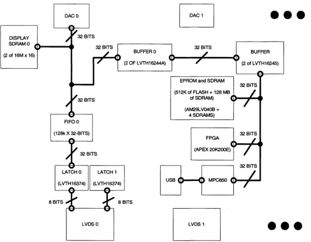
processor of the Mark-II system. These analog outputs are created by 6 digital-to-analog converters (DACs). Data is supplied to these DACs from either the LVDS connection or the USB connection. The data is also stored in SDRAM memory blocks that represent the Video memory of the system. Various FIFO's, buffers, and latches are also placed on the board in order to ensure stable data and avoid issues like bus contention and glitching signals. A basic design of the system is shown below.
DAC 0 DISPLAY SDRAM 0 (2 of 16M x 1 DAC 1 S.. 32 BITS
32 BITS BUFFER 0 32 BITS
BUFFER
6) 1 /A
(2 OF LVTH16244A) (2 of LVTrH16245) EPROM and SDRAM 32BT
(512K of FLASH + 128 MB
32 BITS of SDRAM)
(AM29LVO40B +
4 SDRAMS)
FIFO 0
(128k X 32-BITS) FPA 32 BITS
32 BITS (APEX 20K200E) 32BT LATCH 0 LATCH 1 (VTH1374) (LVTH1374) USB ( MPC850( 8 BITSo8 BITS LVDS 0 LVDS 1
Figure 5: General Block Diagram for Video Concentrator Card
I.
The VCC is designed to support high bandwidths of data. The data bus is 32 bits wide and runs at 50 MHz. The speed of the FPGA is design dependent, but is being run at 48 MHz to match the processor speed. The LVDS interface is 8 data streams wide and achieves data transfer rates of 5.7 Gigabits per sec (Gbps). The USB interface can
receive 16 bits at a time and receives data at 12 Mbps.
3.1.1 Improvements upon Cheops
One of the problems of the Cheops system was that there were several
computation stages, each requiring its own computer. The holographic files were usually rendered separately on a different machine. The data was then fed into a different
machine, which was connected to the Cheops system. If any data needed to be modified or computed in Cheops, another delay was added, until the appropriate data was finally outputted to the RF processor.
Holo-Chidi hopes to improve on this design by combining all these separate machines into one machine. On this machine, the user will be able to render or compute the holographic data, send it immediately to the hardware, which would in turn output the
data to the RF processor. The machine would contain a back-plane that would house the
9 Avid cards and the 3 VCC's. This machine would eliminate the bottlenecks that would
occur when data needed to be transferred to the hardware, and would allow for easier upkeep, since only one host computer would need to be maintained, for data archival and retrieval.
3.1.2 General Design
The Video Concentrator Card needed to be designed from the ground up. The initial board design needed to take place. The initial design also involved selecting all the components that would best suit the design. Numerous components were compared in order to find which ones that had the best properties required for the board. Once the components were selected and purchased and the design was finalized, the boards were sent to an independent contractor (DDI Advanced CAD Solutions). The contractor then created the layout for the board, fabricated and assembled the board with the appropriate parts. Once the board was returned, work began on the verification of the board design, and the programming of the main components of the board. Upon completion, the board will be integrated with the Avid Processor card. Once mated, the two systems will be integrated into the holovideo system.
The design had to be verified for full functionality as well as errors that could hinder the abilities of the board. Functionality, as well as cost effectiveness and space issues, became key points in deciding many of the design decisions. The large number of components required to support 6 channels of data led to the creation of a fairly large board, so any unnecessary components were quickly removed. This work involved researching and selecting the appropriate chips necessary to complete the project. Before it could be sent for fabrication, a netlist was generated, to allow the contractor to properly match signals to their corresponding ports on the components. This netlist also ensured that all the power pins were properly routed, so all of the chips on the board would be supplied with the appropriate power source.
Upon completion, the board ended up having 9 PCB layers. It was heavily populated on both sides. Its size was 6 inches by 12 inches. Due to the variety and complexity of the components, the board requires 4 different power sources to enable all of the chips: 12V, 5V, 3.3V, and 1.8V. The majority of the components require a voltage of 3.3V, keeping the board as low power as possible. With the number of components on the board, power considerations are a key concern. The board must be ideal for use in Holovideo, requiring it to have as low a power source as possible.
3.1.2.1
Cadence Design Software
Before the board could be sent off for fabrication, its complete schematic needed to be designed and verified. Cadence design software was selected as the tool to perform this task. This program gives a point-and-click method of designing complex board schematics. The Cadence software was selected for its ease of use, and wide
functionality. Every component of the board was carefully laid out and connected completely. Once completed, the pins of each of these chips need to be assigned. The software had an excellent debugger, which enabled design mistakes to be caught in the earliest stages of design. The whole system is divided into pages, which each contain a portion of the card, e.g. each DAC controller, along with its buffer and SDRAM, are contained in one sheet. Due to the complexity of the system, the board required several schematics pages of layout, 11 in total. The convenience of the Cadence software
allowed a great decrease in the time needed to complete the schematic layout of the VCC.
3.2
Hardware Functional Blocks
3.2.1 MPC850 Integrated Communications Microprocessor
The Motorola MPC850 was chosen to be the processor for the VideoConcentrator Card. The chip contains a single-issue, 32-bit version of the embedded PowerPC core with 32 x 32-bit integer registers, used for application programming use. This processor is integrated with a communications processor module (CPM), which contains a special-purpose 32-bit scalar RISC communications processor.9 This
two-processor architecture is more efficient than traditional architectures because the CPM offloads peripheral tasks from the embedded PowerPC core. One of the other advantages
of the CPM is that it supports up to seven serial channels, including a universal serial bus
(USB) channel.
MPC Diagram Blo ck M
2 K8
I-aw SYSTE INtAC Ul~f
ins~efen8 Entr
l b aMMU i MMMY Controller
unirodso -I---~ -ibs Intnrere Unit
-SbtestforE ntry o te c
-DatHadlrbscnto s loe at i I
PaasM/O e2 n Dual-Pa
pr o wl s32-bit RISC pC m Tontro IDMA
interfand Program Ro
and r n th i
Port Fins ire
USB
C8SCC*
[SM1
MC2US
PI1C
Tlm* Sot Assignwr SeW Mntface
Figure 6: Block Diagram of the MPC8509
The MPC850 will be in charge of controlling the data bus, through the use of its internal bus arbitration system. The processor will arbitrate between the systems on the board that require the data bus to transmit data. Once the processor releases control of the bus, it waits for the next request for control of the bus, or asserts control itself. Discussion of how the bus control signals work will be reserved for Chapter 5, when the Data Handler bus control system is looked at in greater detail.
The USB port is vital in ensuring the soundness of the design of the VCC. The processor will serves as a verification system. The USB controller that the CPM contains will be used to send data into the VCC system. It will take some time for the LVDS interface with the programmable Avid cards to be fully up and running. Until that section is running, the USB port will allow frames of data to be fed into the system. The CPM will decode this data and, once bus control is gained, the processor will place this data on the main memory. From the main memory, the data is sent to the display memory by the
processor, without fully functioning Avid cards. Full debugging of the VCC can be completed while the Avid boards are still being configured.
In addition to serving as a verification component, the processor might be able to assist the Holo-Chidi system. Holographic video requires an immense amount of
computational power in order to quickly render the frames in real-time. The MPC850 might be used in future projects to assist in that computation. The VCC has been designed to allow flexibility for the researcher to use the great processing power of the processor to assist however they see fit. Future projects could benefit greatly from this flexibility.
3.2.2 Field Programmable Gate Array
The Field Programmable Gate Array (FPGA) is the most important chip on the entire board. The HoloFPGA (holographic FPGA) is the essential control interface for the video concentrator card. It is the programmable device that contains the synthesized VHDL code that will manage the control signals for the entire board. The FPGA will
have the responsibility for moving data through the system, storing the data in the proper locations, and outputting the correct data values to the Holovideo system. The FPGA also has the ability to run different applications at different clock frequencies, which is important when dealing with different components running at different speeds. The Data Handler system, the VHDL system in charge of the VCC control, is implemented inside
the FPGA. The Altera Apex 20K200KE FPGA was selected to control the VCC. This
FPGA has a maximum 526,000 system gates, which consists of 8320 logical elements
(LEs) and 52 Embedded System Blocks (ESBs).10 The FPGA also contains a maximum of 376 user 1/0 pins that are available for use.
The FPGA will function as one of the bus masters on the data bus. It will be able to gain control of the bus. Again, to ensure no bus conflict, the bus controller on the
FPGA needs to closely follow the structure of the controller on the MPC850. Care has to
be given in this design, so neither controller ends up interfering with the performance of the other. With its immense size, the FPGA could also possible assist the processor in computing duties for the data entering the system. It is another tool that greatly improves the flexibility of the system. A full description on general and Altera Apex20K family
specific FPGA architectures is given in chapter 4. Chapter 5 is devoted to the Data Handler system contained within the FPGA.
3.2.3 LVDS Interface
The system incorporates a Low Voltage Differential Signaling (LVDS) standard for point-to-point physical layer interface data transfer. LVDS is a high speed, low power general purpose interface standard that allows for the ability to transfer data at high rates. Through the use of differential signal transfer techniques, LVDS technology delivers the bandwidth necessary for high-resolution displays, while maximizing bit rates.
CMO3/1T OUTPLT3 FED I Th S038 Al pie VSDslyRcieranftudbyNina GRN t A2 8 U ELJ2 tvti NS.). Am t s CR (te C. Ias mxud at x 12 MHz f
(Gbps). It decodes 8 LVDS data streams 48 bits of CMOS/TTL data and 3 control bits. The LVDS connection will be the main method of communication between the Avid cards and the VCC. The computed fringe patterns will be passed through the LVDS connection, to the Display SDRAM and on to the DACs for analog conversion. Three
LVDS receivers are required per board, and each will handle two channels of holographic
data.
The computationally intensive holovideo system requires high bandwidth in order to allow real-time streaming of the holographic frames. The faster the throughput, the faster the frames become available to the Mark-II Display system. In addition, LVDS technology is not dependent on a specific power supply, such as +5V. This means there is an easy migration path to lower supply voltages such as +3.3V while still maintaining the same signaling levels and performance. This is useful for the Video Concentrator Card, since the various chips need different voltage levels in order to function. The
LVDS system enables us to power this variety of chips without worrying about the
integrity of the signal. The LVDS system accomplishes high data rates, low power, and reduced EMI effects by reducing the signal levels.
3.2.4 Digital to Analog Converter
In order for the Mark-II system to function properly, it requires RF analog signals to drive the AOMs. Since holographic data is in a digital format when is arrives at the
VCC, it will need to be converted into an analog format. Also, the analog signals need to
be powerful enough to drive the holographic display. The Texas Instruments TVP3010 Video Interface Palette is the device being used on the board. This device can
accommodate 64-, 32-, 16-, 8-, and 4-bit pixel buses without any additional circuit modifications. The device contains three 8-bit digital to analog converters, which are capable of directly driving a doubly-terminated 75-4 line. The device is also highly system integrated. It did not require any external buffer logic when connected with the data bus. External buffers were utilized, only to detach the two data bus paths for the inputs from one another, in an effort to avoid possible bus contention.
3.2.5
SDRAM
The SDRAMs, or Synchronous DRAMs, are the main storage component of the
VCC. This is where the frames will be stored and made available for output or
manipulation. The Micron MT48LC16M16A2 256 Mb SDRAM was selected for the system. It contains 4 banks of 4 Megabits (Mbs), each 16 bits deep. This component was selected for its ease of use, fast writing times, and for its storage locations of 16 bits.
Two of these memory chips are enough to handle a 32-bit data bus. Another major benefit of this SDRAM is its allowance of burst reads and writes. A burst transfer means that accesses start at a selected location and continue for a programmed number of locations in a programming sequence.13 The burst lengths of 1, 2, 4, or 8 locations, or the full page is programmable for the READ or WRITE operations. This allowance for synchronous burst data transfers at high speeds is essential for efficient data transferring within the Video Concentrator Card. The quicker data can be stored, the faster it can be outputted, or made available for possible computational purposes. The SDRAMs are divided into two sections on the board: main memory and video memory.
3.2.5.1
Main Memory
The Main Memory is a bank of 4 SDRAM's connected to the data and address buses. These buses are accessible to both the FPGA and the processor. The main purpose of this memory is to store frames of data that enter the system through the USB port. Data is stored in the SDRAM, and then it is outputted to the DACs. This SDRAM is initially used for verification of the VCC system. Eventually, these memory banks can be used to assist the processor and the FPGA with its processing potential. Frames can be stored in the main memory, in order to be accessible by these devices for computation
or manipulation. This is another level of flexibility that gives the VCC great potential to become more than a simple frame buffer.
3.2.5.2
Video Memory
The video memory is also known as the display SDRAM. This section of memory is responsible for actually storing frames as they enter from either of the input
interfaces. The data is passed on to the DACs for conversion to analog format. There are 12 SDRAMs on the board that make up the display SDRAM. Each channel has two associated SDRAMs. Two were necessary for the 32-bit streams of data, since the SDRAM can only store 16-bits at any given location. Each holo-line will store data on these SDRAMs to allow for error recovery and better streaming of holographic frames
3.2.6 Flash ROM
The main purpose of the Flash ROM is to contain the boot code for the processor. The processor will not be able to function unless it is loaded with the proper
programming. The Am29LVO40B is 4 Megabits (512K x 8-Bit), composed of eight 64 Kbyte sectors, that operates at low power levels.14 Also, any combination of these sectors can be erased, including the full chip. One problem with the ROM is that it outputs only 8 bits for any address, even though the rest of the system, including the processor, runs on a 32-bit bus. So, 4 addresses were required in order to receive one full command for the MPC850. The Flash ROM has an access time as fast as 60 ns.
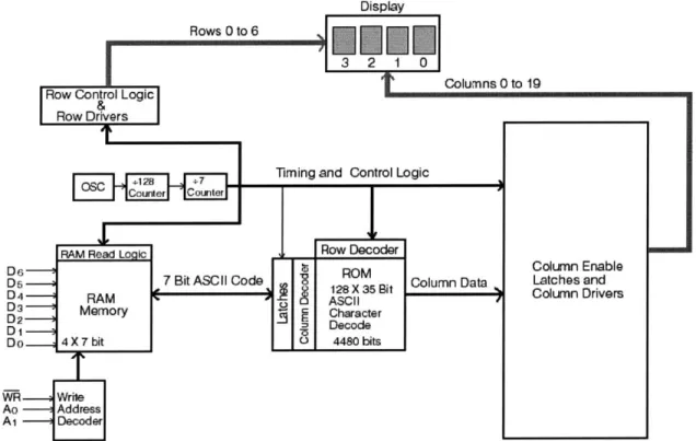
3.2.7 Alphanumeric Display
The alphanumeric display is one of the main tools to test the functionality of the system. It displays data on 4 display modules that can display 5x7 dot matrix characters. It contains RAM memory to allow displayed data to be stored until over-written by newer data. The Infineion DLO-1414 alphanumeric display has to ability to output 128 special
ASCII characters. 15 For the purpose of testing, the board only requires the display to show hexadecimal numbers.
to 19
Display
Rows 0 to 6
, 1 11 1
3 2 1 0
Row ConCrol Logic dColumns 0
Row Drivers
T
0SC
-028e +7ute Timing and Control LogicRAM Read Logic _Row Decoder
D6 ROM
D E 7 Bit ASCI I Code Column Data
D 4 RAM C 35 Bit Memory gCharacter D1i Decode D o 4 X 7 bit 4480 bits WR Write Ao Address Ai Decoder
Figure 8: Alphanumeric Display Block Diagram5
Column Enable Latches and Column Drivers
With this device, the actual state of the system can be viewed. Two of these displays were used on the board. Using these 8 character displays, any set of signals could be viewed. As the system operates, the addresses to which the holographic information is being written can be displayed, or the data that is actually being
transmitted. This flexibility improves the ability to verify the functionality of the board at a faster pace.
3.3 Implementation
Once these functional blocks were selected for the VCC, they needed to be
acquired and assembled on the board. Upon completion of the assembly, the boards were then ready to be tested. The initial power up and test of the board proved that it was running at full power and all of the components were on. Now, the focus of the projected shifted to the development of the data processing subsystem that would control the functions of all the hardware.
Chapter 4: System Control Logic
In order to understand how to design a control system for the VCC board, one must first understand what designing a system entails. A specific methodology must be set in order to avoid confusion and allow for a stable design. The tools required for such a task must be studied and understood to allow the design to function at peak efficiency. The device on which the design will be placed must be looked at as well. Every device has its own abilities, which can benefit and also hinder design efficiency.
4.1
General FPGA Overview
The device that we will be using to handle the control design for our board is an
FPGA, or Field Programmable Gate Array. An FPGA is essentially a two-dimensional
array of programmable logic cells. These cells can communicate with one another and also with 1/0 pins connected to the device. Through the use of routing wires, or
channels, the different programmable elements can communicate with one another in the device. A programmable, switching network, known as interconnects, are placed in a grid-like structure made of vertical and horizontal columns. These interconnects can be enabled or disabled to create logical communication paths between the logical cells. The channels also connect the logic cells to the 1/0 pins that enable the programmed logic to interface with the rest of the system.
FPGAs have many desirable qualities that are essential for the efficient operation of the VCC. Reprogrammability is one of the most important benefits. FPGAs can be reprogrammed hundreds of times, which is important when debugging a design. If this option did not exist, it would be impossible to implement a perfect design on the first attempt. Also, due to the flexible nature of the duties of the FPGA in the VCC,
reprogrammability allows the researchers to experiment with how it is used in the system. FPGAs are versatile devices. They can handle multiple designs within its logical
structure. In the VCC, the FPGA will need to handle the control logic of the system, but could also contain some processor functions, if desired. Since all of these abilities fit within one device, space on the crowded VCC is saved.
Though ideal for the VCC, FPGAs do not come without their share of drawbacks. Timing analysis of an FPGA can prove to be difficult. Signal propagation delays become a function of the number of cascaded logic cells, the number of programmable
interconnects through which the signal propagates, the technology used to design the system, fan-out, and 1/0 cell delays.16 If this information cannot be determined, accurate estimates of system performance and propagation delays will be difficult to ascertain. Software packages that contain static timing analyzers can assist in determining these values.
There are many manufacturers of FPGA's. Xilinx, Altera, and Lucent are some of the more commonly known ones. An Altera device was chosen as the FPGA for the
VCC. Several factors contributed to this choice. Altera devices are inexpensive, relative
to the amount of gates contained on the device. The designers of the VCC have some experience with Altera products and software packages. This allows design,
implementation, and verification to be completed in a faster time frame. Also, the Altera chips are incredibly flexible, as they can be implemented to hold standard logic, or to act as memory, through the use of the Embedded System Blocks (ESBs).
4.2
Altera APEX 20K200E Design
4.2.1 Overview
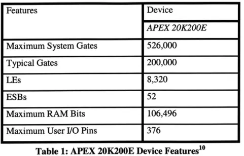
The APEX 20K200E device, containing 526,000 system gates, is designed with the Multicore architecture, which combines look-up table (LUT)-based logic, product-term-based logic and memory into one package. LUT-based logic provides optimized performance and efficiency for data-path, register-intensive, mathematical, or digital
signal processing designs. Product-term-based logic is optimized for complex
combinatorial paths, such as complex state machines. Applications involving all three forms of logic can be integrated in the FPGA. Embedded system blocks (ESBs) are used to implement memory and product-term-based logic, while logical elements (LEs) are used when implementing LUT-based logic. Table 1 summarizes the features of the APEX 20K200E.
Features Device
APEX 20K200E
Maximum System Gates 526,000
Typical Gates 200,000
LEs 8,320
ESBs 52
Maximum RAM Bits 106,496
Maximum User 1/0 Pins 376
Table 1: APEX 20K200E Device Features"
The signal interconnections, within the device and with the 1/0 pins, are implemented using the FastTrack Interconnect system. It is a series of fast, row and column routing channels that run throughout the length and width of the device.'0 A block diagram
relationship between all these components is shown in Figure 9.
Four-inputWT
fordab path and
DSP fundkm. Prcviuct-rm integrafion Ar hkh-speedi cwikvibocand FatTack 4tecomet 1mory mo moy I 10ds suppOft PCI, GTL+, SS A-L 0VE, and other standadl. Fleible integra in of embeJdd menoyindudlng CAM, RAM,
ROA( FIR and
othermenmy funcions
Figure 9: APEX 20K200E Device Block Diagram"0
Due to the large number of components on the board, an FPGA with enough I/O pins to connect to all of the control ports of these devices was required. With its 376 user I/O pins, the APEX 20K200E was ideal for the unique and demanding requirements of
ClxkMa mgement Circuby
Ll
Ll
I I
The Data Handler data processing system was implemented with the APEX 20K200E. The FPGA has enough gates to not only implement this system, but also to allow for further research possibilities as other designs can be included in the device. This FPGA provides the entire board with flexibility necessary in a research
environment.
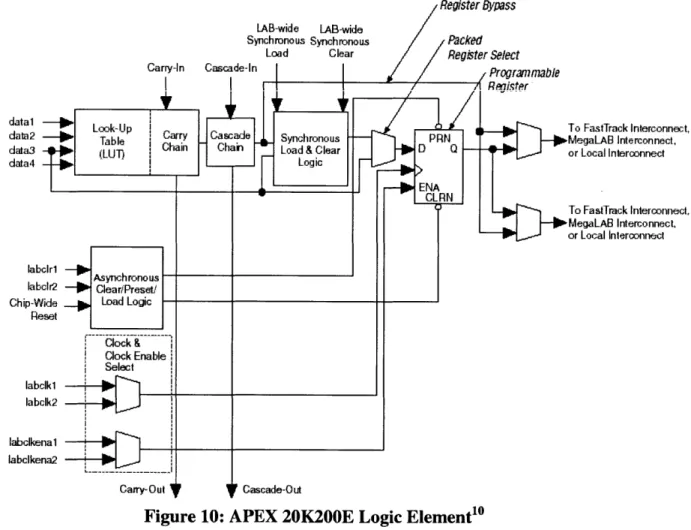
4.2.2 Logic Elements
The logic cell, the basic unit of a FPGA, is implemented as a Logic Element (LE) in the APEX 20K200E. Each LE contains a input LUT, which can implement any 4-input function. 10 LEs compose a logic array block (LAB). Figure 10 gives the basic structure of the LE and how it connects to the various interconnects.
LAB-wide LAB-wide Synchronous Synchronous
Load Clear
Carry-in Cascade-In
datal -4 Look-Up
data2 -- Table 1 Carry Cascade Synchronous
data3 LUT)LW Chain Chain Load & Clear
data4) Loi Register Bypass Packed Register Select Programmable Rmister PAN I D NQ -To FastTrack nt MegaLAB Intero or Local lnteroon - ENA CLAN To FastTrack Int MegaLAB Interc or Local Interoon labclr1 4Asynchronous labcIr2 Clear/Preset! Chip-Wide Load Logic
Reset -Clock & Clock Enable Select labelki Iabclk2 labclkenal _ labclkena2 Cany-Out Cascade-Out
Figure 10: APEX 20K200E Logic Element0
Each LE contains a programmable register, which can be configured for D, T, JK, or SR operation.10 For combinatorial functions, a bypass exists to allow the LUT to directly
erconnect, onnect, nect erconnect, onnect, nect
chains. Without using the interconnect resources, adjacent LEs are grouped together. This feature is useful when designing high-speed adders, counters and wide fan-in functions.
4.2.3 Embedded System Block
Embedded System Blocks (ESBs) can be used to implement product-term logic and several memory functions common to logical designs. These functions include common storage devices, such as context-addressable memory (CAMs), RAMs, dual-port RAMs, ROMs, and FIFOs. ESBs contain input and output registers that are useful when
implementing memory. The input registers synchronize writes and the output registers can pipeline designs to improve system performance. ESB memory can be configured in
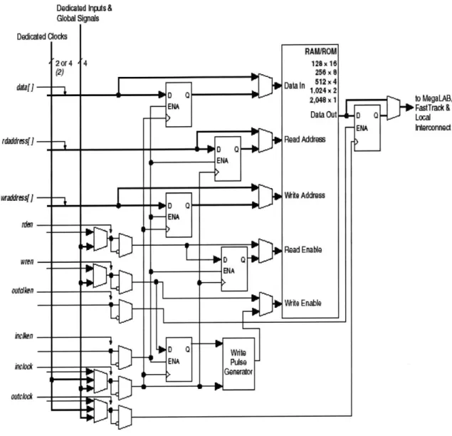
5 possible sizes: 128x16, 256x8, 512x4, 1024x2, 2048x1. By combining multiple ESBs, larger memory blocks can be implemented. A block diagram of an ESB module is located in Figure 11.
Dedicated Inputs& Global Signals Dedicated Clocks
I
2or4 (2) ~~1 4 4 D 4-j-- ENA D Q ENA~LD~
RAWROM 128x 16 250 x 0 Dataln 1024 2,04,8 x 1 Data Out Read Address Yite Address Read Enable rite EnableKrifl
Pulse --Generalor to MegaLAB, Im~hatTrack & Z DO Local r ENA InterconnectFigure 11: APEX 20K200E ESB in Input/Output Clock Mode'0
In the previous chapter, the use of the FPGA as a flash ROM was mentioned. ESBs can implement logic functions when programmed with a read-only pattern during configuration, creating a large LUT. In order to store the boot code for the MPC850, the
FPGA needed to create a 4096x32-bit ROM using the ESBs. The actual implementation
of this ROM will be discussed in Chapter 5.
4.2.4 FastTrack Interconnect
FastTrack Interconnect provides connections between all of the APEX 20K200E elements. By using a global routing structure, this form of interconnects avoids the pitfalls that accompany a segmented routing scheme. In a segmented routing scheme,
rdM&rs)j -vffl -oddrikn -ixkn
-i::, I i
b D 0 Pop F ENA 101 D ENAswitch matrices connect variable routing paths, which can lead to increased delays and a decrease in efficiency. A global scheme results in predictable performance, even in complex designs. In the APEX 20K200E, FastRow interconnect creates faster routing of input signals. It is driven by column I/O pins, without the need to use the LAB
interconnect, by routing it directly to the local interconnects. This enhanced structure, detailed in Figure 12, is useful when the input signals have a high fan-out, which occurs when it needs to drive multiple outputs.
FastRow Intecomect Drives Local Intrconect In Two MegaLAO Siftures
[oE
TOE
SelectVelid YO PInand FastRow ~~ii; Intemcnet *0 0 4-\J-I II 0*S 4-Afl S
MegaLAB LAS MeCLtnD
Figure 12: APEX 20K200E FastRow Interconnect0
Local IntMwflflct
4.3 Software
After gaining a good understanding of the inner workings of the FPGA, the
methods through which a design will be created need to be studied. The most appropriate design methodology is one that increases the efficiency of the designers. It must
facilitate capturing, understanding and maintaining a design. It must be able to support
FastRow Intrconect
--- -
------
complex designs with hierarchy and gate-level to system-level design. It should have the flexibility to support multiple levels of design description.
There are two hardware description languages (HDLs) that satisfy these digital design requirements: Verilog and VHDL. Verliog is less verbose than VHDL, but it can be argued that this is at the expense of language richness and features.1 6 For the purposes of documentation, synthesis, and simulation for both devices and systems, VHDL is the best choice for the VCC.
4.3.1 VHDL
VHDL stands for VHSIC (Very High Speed Integrated Circuits) Hardware Description Language. It has powerful language constructs that can be used to write efficient code descriptions of complex control logic. The language is highly portable, meaning synthesized designs can be simulated. Since the language is common in industry, multiple software packages have the ability to read and synthesize it.
There are some shortcomings associated with VHDL. The control of the definition of the gate-level implementation of circuits is lost to high-level abstract concepts. Fortunately this is not a problem that greatly affects most designers. Most modem synthesis tools give some level of control over the implementation, especially to make area-efficient versus speed-efficient choices. Also, logic implementations created
by synthesis tools are relatively inefficient. These synthesis tools are designed to be
generic in nature. Compilers use algorithms to decide upon logic implementations, following standard design methodologies. These implementations might not always be optimized for a specific design, since the tools are meant to work with all designs and not a specific one. This problem can be fixed by creating efficient code. Inefficient code can lead to unneeded, repetitive, or nonoptimal logic.
The Data Handler system is implemented in VHDL. For the purposes of creating the system level control logic, VHDL was a sufficient language. The designers of the project were also very familiar with the language and had experience using it to designing large systems. This led to a more efficient design process, easier debugging, and better optimizations, leading to a timely completion of the project. Quatus II was the best package for the development of the Data Handler system, since Altera also built the