HAL Id: hal-02324983
https://hal.univ-grenoble-alpes.fr/hal-02324983
Submitted on 30 Nov 2020HAL is a multi-disciplinary open access
archive for the deposit and dissemination of sci-entific research documents, whether they are pub-lished or not. The documents may come from teaching and research institutions in France or abroad, or from public or private research centers.
L’archive ouverte pluridisciplinaire HAL, est destinée au dépôt et à la diffusion de documents scientifiques de niveau recherche, publiés ou non, émanant des établissements d’enseignement et de recherche français ou étrangers, des laboratoires publics ou privés.
Engineering Self-Assembly of a High-χ Block Copolymer
for Large-Area Fabrication of Transistors Based on
Functional Graphene Nanoribbon Arrays
Javier Arias-Zapata, Jérôme Daniel Garnier, Hasan-Al Mehedi, Antoine
Legrain, Bassem Salem, Gilles Cunge, Marc Zelsmann
To cite this version:
Javier Arias-Zapata, Jérôme Daniel Garnier, Hasan-Al Mehedi, Antoine Legrain, Bassem Salem, et al.. Engineering Self-Assembly of a High-χ Block Copolymer for Large-Area Fabrication of Transistors Based on Functional Graphene Nanoribbon Arrays. Chemistry of Materials, American Chemical Society, 2019, 31 (9), pp.3154-3162. �10.1021/acs.chemmater.8b04936�. �hal-02324983�
Engineering self-assembly of a high-χ block
copolymer for large area fabrication of
transistors based on functional graphene
nanoribbon arrays
Javier Arias-Zapata,
∗,†,‡Jérôme Garnier,
†Hasan-Al Mehedi,
†Antoine Legrain,
†,¶Bassem Salem,
†,§Gilles Cunge,
†and Marc Zelsmann
†,k†Université Grenoble Alpes / CNRS-LTM / CEA-LETI-MINATEC Campus, 17 rue des Martyrs, F-38000 Grenoble, France
‡Orcid ID: 0000-0002-0566-0222 ¶Orcid ID: 0000-0003-2702-6721 §Orcid ID: 0000-0001-8038-3205 kOrcid ID: 0000-0002-7619-4871 E-mail: javier.arias-zapata@univ-grenoble-alpes.fr Phone: +33 (0)4 38 78 92 92. Fax: +33 (0)4 38 78 58 92 Abstract
Graphene presents a real need for patterning into very narrow nanostructures to open up a bandgap and tune its electrical properties by quantum confinement. A self-assembled silicon-based block copolymer (BCP) is used to pattern CVD-grown graphene to fabricate graphene nanoribbon (GNR) arrays. Best BCP lithographic performances are obtained when the BCP is spin-coated and annealed directly on graphene. Self-assembly on large surfaces (1 cm2) is achieved in a few minutes and 11-nm-width GNR
are finally obtained. Electrical characterization of these structures such as bandgap opening is carried out to confirm the electronic behavior of the graphene nanoribbons. Bandgap values of the order of 70 meV were measured. The BCP self-assembly pro-cess proposed is scalable and low cost, and is well-suited for integration with existing semiconductor fabrication techniques. The lithography procedure developed in this in-vestigation could be generalized to fabricate graphene nanomeshes or quantum dots on large surfaces. Also, other 2D materials and heterostructures could be concerned, for to the study of innovative nano-structured materials and functional devices.
Keywords
CVD graphene, PS-b-PDMS, self-assembly, nanolithography, nanoribbons, field-effect tran-sistor
Introduction
Block copolymer (BCP) lithography builds up nowadays as a surrogate patterning technique capable of producing efficiently sub-10 nm features. Among its counterparts, e.g. electron-beam, ion-electron-beam, deep UV and multiple patterning lithographies,1–3 BCP lithography has a
large advantage in terms of cost of implementation, scalability and throughput. These three factors are essential to fulfill and exploit the current demand in applications needing ultra high-resolution patterning.
BCP lithography is based on a thermodynamics-governed self-assembly mechanism. In equilibrium conditions, BCPs macromolecules self-assemble into ordered periodical struc-tures,4 which can be used as lithography masks for device fabrication. The opportunity
to create sub-10 nm periodical lengths is closely linked to a larger chemical incompatibil-ity between the polymer blocks. This contrast is usually designated as the Flory-Huggins interaction parameter χ by the BCP theory.5
Lately, research on BCP synthesis has been focused on high-χ systems, to name a few:
poly(styrene)-block-poly(4-vinylpyridine) (PS-b-P4VP), poly(styrene)-block-poly(dimethylsiloxane) (PS-b-PDMS) and poly(1,1-dimethylsilacyclobutane)-block-poly(styrene) (PDMSB-b-PS).6–8
They all aim to replace a first generation of BCP systems such as poly(styrene)-block-poly(methyl methacrylate) b-PMMA)and poly(styrene)-block- poly(ethylene oxide) (PS-b-PEO) with rather low-χ values (χ < 0.1 at 298 K) limiting the attainable resolution to around 15 nm.9
Apart from resolution, a high etching selectivity make PS-b-PDMS thin films technolog-ically attractive as performant templates for nanolithography. A high assembly kinetics is attainable through thermal annealing for PS-b-PDMS having low molecular weight. Never-theless, the use of PS-b-PDMS faces issues concerning the domain orientation control due to a high surface energy constrast between the blocks (γP S = 40.7 mJ/m2 vs. γP DM S =
19.8 mJ/m2).10,11 Consequent difficulties in obtaining the desired equilibrium morphology
and stacking of the BCP thin film were solved by a functionalization of the substrates with hydroxy-terminated polymers.
Within the context of emerging 2D materials, among them graphene and transition metal dichalcogenides,12,13 PS-b-PDMS nanolithography encounters further challenges. 2D
materi-als need high-resolution patterning as an effective method to enhance a specific property.14,15
Such is the case of the electronic bandgap in graphene through an accurate structuration.16
PS-b-PDMS self-assembly on atomic-thick substrates establishes proper constraints in the morphology control since the usual functionalizations could irreversibly damage their struc-tural and electrical properties. For this reason, dealing with graphene requires special con-sideration regarding its physico-chemical state during the self-assembly process as well as a critical dimensional characterization on an atomic scale during patterning.
The few studies that have been conducted on the self-assembly of cylindrical PS-b-PDMS on CVD-grown graphene to produce graphene nanoribbons (GNR)17–19 usually use the
thermal annealing as an effort to exploit the PS-b-PDMS on manufacture-adapted proce-dures.20,21 In this context, additional investigations are required on the self-assembly
mech-anism on graphene. It includes the searching of the equilibrium conditions at which the cylinder morphology can be obtained on large surfaces to guarantee the ensuing develop-ment of GNR-based devices.
This study aims at investigating the cylindrical PS-b-PDMS self-assembly on CVD-grown graphene by thermal means to produce GNRs arrays over large areas. Across the study of the BCP/graphene interface and their interactions, we highlight how the chemical state of the CVD-grown graphene impacts on the sensitive self-assembly process. Dealing with a graphene surface energy modification through a thermal pre-annealing, we achieve a mor-phology control of the PS-b-PDMS thin film adapted for nanolithography without altering the graphene properties. Furthermore, the large-area patterning of graphene is shown with an exhaustive characterization. Finally, the development of back-gate field-effect transistors (FET) based on GNRs arrays allowed to verify the effect of the graphene structuration on its conductive properties with the transition from metallic to semiconductor behavior.
Experimental section
Graphene and block copolymer
Monolayer CVD-grown graphene on 300-nm SiO2 on P++ < 100 > Si 4-in wafer, was
obtained from Graphenea (Spain); usually transferred by a wet transfer process. The graphene/SiO2wafer was carefully cleaved into 1 cm2samples. Cylinder-forming PS-b-PDMS
BCP (Mw=11-5 kg/mol, PDI=1.08, fPDMS=33%) were purchased from Polymer Source Inc.
(Canada) and microelectronic-grade propylene glycol methyl ether acetate (PGMEA) was used as the solution solvent. A BCP monolayer was deposited directly on the CVD-grown graphene. For this, a BCP solution of 1 wt% was spin-coated at different spin speeds. The final BCP thickness and the spin speed were correlated by ellipsometry measurements and
estimated at 18 ±2 nm for 1800 rpm. A vacuum drying oven at 10−3 mbar was used for
graphene surface energy modification as well as a hot plate for annealing treatment at differ-ent temperatures and time to achieve the cylinder-forming self-assembly of the BCP. After thermal annealing, samples were first etched by CF4plasma (6 s, 4 mTorr, 500 W) to remove
the top-segregated PDMS layer; then a HBr/O2 plasma (14 s, 5 mTorr, 150 W) etched both
the PS block and the unexposed graphene. BCP mask stripping was performed with HF and GNRs cleaning with H2 plasmas (20 s, 200 mTorr, 800 W).
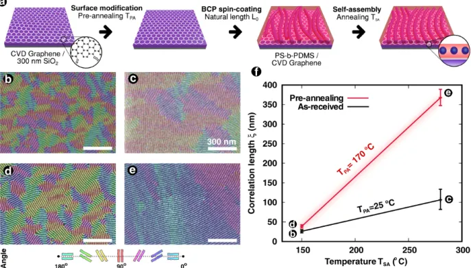
Fig. 1 resumes the entire procedure developed in this study in order to perform the self-assembly of a PS-b-PDMS BCP to obtain a lithography mask for graphene patterning. This method allows an effective large-area integration of FETs based on dense 11-nm-width GNR arrays. Our strategy includes: (1) the use of CVD-grown graphene on 4-inch wafers deposited on 300nm-SiO2, which is suitable for large-scale device fabrication; (2) eventually
the annealing of CVD graphene on SiO2 under vacuum (10−3 mbarr) for surface energy
modification at 170 ℃ for 1 h and finally (3) the direct spin-coating of the PS-b-PDMS solution and its thermal annealing for 3 min, enabling spontaneous phase separation and formation of densely packed periodic arrays of cylindrical BCP nanodomains.
Characterizations
Observations. Scanning electron microscopy (SEM) images were performed at 30 kV with a field emission electron source (Hitachi S-5000). Sample preparations for transmission electron microscopy (TEM) were carried out in a Helios 450S-FEI dual beam microscope. A small sample was extracted and thinned to approximately 100-nm-width, after the deposition of 1-µm-Pt on the BCP thin film. An in-situ observation was finally carried out using in scanning mode (STEM) in the same equipment or a JEM-2100F instrument was used for TEM observations at an electron acceleration voltage of 200 KV.
Contact angle. Static contact angles were measured by the drop shape analyzer DSA100 from Krüss (Germany). All measurements were performed at room temperature (25 ℃) by
depositing a water droplet with 7 µL volume on the surface. The contact angle was measured based on the image captured by a CDD camera using the ADVANCE software.
X-ray photoelectron spectroscopy. The chemical state of CVD-grown graphene was studied by XPS with a customized Thermo Electron Theta 300 spectrometer. Measurements were achieved at a pressure of 10−9 mbar using a monochromatic X-ray source Al-Kα (1486.6 eV).
An electron flood gun was turned on during acquisitions to reduce surface charging. The overall energy resolution of the analysis was 0.5 eV. CASAXPS software was used for fitting the C1s peak.
Raman spectroscopy. Raman mapping of GNRs arrays was performed using the LabRAM HR Evolution equipment from Horiba Scientific. Measurements were performed using a 70x objective with a green laser having an excitation wavelength of 532 nm. The laser power was 4 mW and the acquisition time was of the order of 30 seconds. Lateral focus of the laser was ∼ 1µm. Mapping area was 100 µm2, scanning from 0 to 10 µm in both x and y directions
with a step of 2.5 µm.
Atomic force microscopy. The GNRs arrays were characterized dimensionally by an AFM Bruker Dimension FastScan, using the automatic mode with a Si tip. Typical parameters for image acquisition used here were 512 lines with a scan rate of 1.98 Hz. Scan size of images was 1 µm2− and the image treatment was performed using the software Gwyddion
(http://gwyddion.net/). Electrical measurements
The photolithography transferred pattern method (PTP method) was used to directly de-posit metallic contacts on GNRs as follows: a Si < 100 > P++ sacrificial substrate was cleaved in 1 cm2 from 4-in wafers. Then a positive photoresist AZ 1512HS from
Microchem-icals GmbH, Germany, was spin-coated on Si samples. After UV exposition, photoresist was developed in AZ 1:4 developer solution to remove the exposed zones. Deposition of 100 nm of Au was achieved with a PLASSYS, France, equipment in clean room conditions. Au
on resist was lifted-off for 1 h with acetone and a final rinsing with iso-propanol. A second stage consisted in spin-coating PMMA A9 from Microchemicals directly on Au contacts. The PMMA/gold layer was then detached from the substrate with a substrate etching in NaOH 1M solution at 50 °C until complete detachment. The PMMA/gold film was then transferred and placed on the GNRs sample surface and the stack was dried in the air. Several cycles of 30 s in acetone, 10 s in iso-propanol and N2 flow drying were repeated until PMMA removal.
Finally a soft-bake at 100 °C for 1 h in vacuum (10−3 mbar) to build contact bonding with
GNRs was required.
The contacted sample was finally composed of a P++ (100) Si substrate, a 300-nm silica film, patterned graphene and 2 on-top Au contacts separated of 2 µm. This stack constitutes the back-gated FET used to prove the bandgap opening in GNR arrays. Electrical measure-ments were performed with a Keithley 4200-SCS equipment. Samples were characterized with the IDS vs. VDS curve from +0.5 V to -0.5 V at a fixed VG = 0 V, and then with
the transcharacteristics curve IDS vs. VG from +30 V to -30 V at a constant VDS = 0.2
V. VDS and IDS are defined as the voltage and current between transistor drain and source,
respectively.
Results and discussion
Self-assembly of PS-b-PDMS
The typical morphology obtained when using the PS-b-PDMS BCP (Mn =16kg/mol, fPDMS
= 33%) is PDMS cylindrical microdomains in a PS matrix. We chose to work with this asymmetric polymer because it allows the formation of objects . 10 nm with a natural period of 20 nm (L0),22 which is interesting for graphene patterning.
The self-assembly behavior of the PS-b-PDMS was studied directly on CVD-grown graphene samples. A direct spin-coating of the BCP on graphene was used to avoid underlayers such as resists, brush polymers or even insulator materials.23 Also, we found that direct
spin-Figure 1: (a) Graphic representation of the CVD-grown graphene patterning on large sur-faces through thermal modification of the surface energy, direct spin-coating of the high-χ BCP PS-b-PDMS and its cylindrical self-assembly by thermal means. (b-e) Top-view SEM images of the self-assembled PS-b-PDMS and their corresponding orientation maps. (f) Cor-relation lengths (ξ) from the orientation maps measured at different self-assembly annealing temperatures (TSA), eventually with a thermal pre-annealing treatment at TPA = 170 ℃.
coating was more efficient than using transfer layers, in particular at the resist stripping step. Indeed, this step is critical as GNRs could be damaged or contaminated, impacting their electronic properties.
Hereinafter, two different annealing temperatures need to be defined. First, the temper-ature of pre-annealing (TPA) for graphene surface energy modification, performed in vaccum
to avoid graphene oxidation. Then, the temperature of self-assembly (TSA) used in air to
trigger BCP organization. Latest advances on the self-assembly of the high-χ BCPs show an improvement in the microphase ordering of the PS-b-PDMS with a defect reduction by shortening time and increasing annealing temperature (300 ℃ < TSA < 700 ℃).24,25 We
studied the effect of higher temperatures on the final microphase ordering by annealing up to TSA=280 ℃. We used this upper temperature to avoid any degradation of the graphene
properties, as thermal stability in graphene has been observed up to 300 ℃ both in standard cleanroom atmosphere.26,27
For a better legibility of pattern ordering and grain sizes, orientation mappings are dis-played in each SEM image of Figs. 1b-e. Moreover, the measurement of the correlation lengths (ξ) are depicted in Fig. 1f, as this parameter allows to quantify the microphase ordering.
When using TSA=280 ℃, a cylinder-morphology is achieved (Fig. 1c) as expected, with
ξ mesured at 106 nm. This result shows a light improvement in the microphase ordering, in comparison with a lower temperature to generate self-assembly. Fig. 1b shows the top-view SEM image at TSA=150 ℃, corresponding to ξ = 26 nm. Despite an improvement in the
microphase ordering by increasing the annealing temperature, both correlation lengths are just a few times the natural lenght L0 which is considered a poor self-assembly (ξ . 100
nm).
In thin film, the self-assembly process is dominated by a significant interface free energy contribution (Finterface) to the total free energy F of the BCP thin film.28In our case, interface
and the orientation of the blocks. Modification and control of the graphene surface energy should allow a precise control of the wetting, BCP orientation and long-range order. Indeed, Kim and coworkers reported a morphology control of BCP thin films by reducing thermally graphene oxide films.29
Similar to graphene oxide reduction, we achived a thermal pre-annealing of CVD-graphene substrates to deal with surface energy modification. As a reminder, PMMA is commonly used as a graphene transfer carrier polymer from Cu growth substrate to the target sub-strate (SiO2 in this case).30 A PMMA coating forms covalent bonds with graphene,31 which
changes significantly the graphene surface state from what it is theoretically predicted.32
Moreover, molecular absorption of H2O and O2 molecules and carbon contaminants from
air during graphene processing could impact its properties33 . Actually, received graphene
surfaces behave rather as a PMMA surface, as evidenced by contact angle measurements (Fig. S1); the graphene surface is rather hydrophilic.
Indeed, by a thermal annealing treatment at 170 ℃, an inversion of the surface character from hydrophilic to hydrophobic is achieved, which is rather a characteristic of the mechan-ically exfoliated graphene.34 We verified this through contact angle measurements with a
water droplet, where the average contact angle changed from 68.1° before thermal treatment (inset in Fig. 2a) to 94.8° (inset in Fig. 2b). The thermal treatment is expected to partially remove water and some of the polar functional groups situated at the extreme surface which favor water wetting.29Fig. 2 confirms this statement by the deconvolution of the C1s peak of
XPS measurements. By heating graphene in vacuum, the amount of carbon-oxygen species such as C-O (∼ 286.5 eV) and O-C=O (∼ 289 eV) is seen reduced in comparison to the as-received graphene, as well as the C-C or C-H peaks (∼ 286 eV) from organic impurities.35
Beyond TPA=170 ℃, significant changes in the graphene surface were not observed. This
was also verified by XPS and contact angle measurements. Main C-O and carbon contami-nants are efficiently already removed at TPA=170 ℃ and produces a significant surface energy
modification. Meanwhile, grafted molecules on graphene, such as PMMA, are not removed. the
Non-thermal methods have been proposed to efficiently PMMA clean graphene.36 However
it goes beyond the scope of this study.
When using TPA=170 ℃ as temperature of pre-annealing, the microphase ordering of the
PS-b-PDMS thin film did not confirm significant changes at TSA=150 ℃ (ξ = 39 nm for Fig.
1d). In contrast, the result of the self-assembled BCP thin film at TSA=280 ℃ is shown
in Fig. 1e. Correlation length value calculations demonstrated a large improvement in self-assembly (ξ = 330 nm), ten times higher than the one obtained in Fig. 1e. In summary, the ordering rate of the BCP is increased with the temperature annealing TSA when a previous
thermal treatment at TPA=170 ℃ is accomplished. Indeed, when increasing the temperature,
the activation energy ∆Ea of the chain diffusion is reduced. In this way, the equilibrium
ordered structure of the BCP thin films is achieved more rapidly,37 which explains the
significant shift in the correlation length observed in Fig. 1f.
Surface energy modification of the CVD-grown graphene
Graphene surface energy modification allows engineering self-assembly through two effects. On the one hand, self-assembly kinetics is enhanced, as shown in Fig. 1. On the other hand, it offers control over the preferential wetting of graphene by the individual blocks of the BCP.
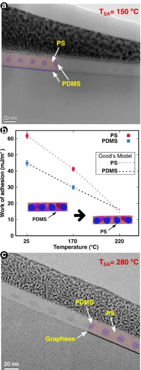
Indeed, we observed the BCP-graphene interface by TEM in order to experimentally de-termine the preferential wetting of the blocks. Despite the significant change in the graphene surface energy at TPA=170 ℃, PDMS maintains wetting graphene at the BCP-graphene
in-terface when TSA=150 ℃ is used to trigger self-assembly (Fig. 3a), which is problematic for
lithography applications.
The work of adhesion W between the graphene surface and one of the polymer blocks is defined as
Figure 2: Thermal annealing of graphene to favor self-assembly of PS-b-PDMS. Contact angle θ and the C1s peak XPS measurement of (a) the as-received CVD-grown graphene and (b) after thermal annealing at TPA= 170℃.
where γP represents the graphene-polymer interfacial energy and Θ is their expected
wet-ting angle on graphene. Using experimental θ values (Fig. 2) and the Good and Girifalco model estimation of the interfacial energy,38 it is possible to estimate the work of adhesion
between graphene and PS or PDMS. Calculations of W are detailed in the Supporting Infor-mation. Experimental W values are displayed in Fig. 3b, as a function of the temperature, as well as Good’s model tendency.
The W values gives important information about the preference wettability of the blocks as a function of the wetting angle. In both contact angles θ measured (fig. 2), a lower W was calculated for the PDMS block. As a result, the PDMS wetting corresponds to the minimal energetic configuration. Clearly, the Good’s model shown in Fig. 3b that the polymer wetting of graphene is expected to change the graphene wetting at higher temperatures: the PS wettability tends to be energetically more favorable for temperatures higher than 220 ℃. Based on the above discussion on wettability of graphene, at higher temperatures a much greater vacuum is needed in order to avoid graphene oxidation, sacrifying throughput. More-over, at higher temperatures than 170 ℃ the graphene surface did not experience important changes in terms of surface energy. These are the reasons why TPA was limited to 170 ℃ but
rather TSA was increased up to 280 ℃ at which the BCP coating protects graphene from
oxidation.
At this temperature, we observed that the PS matrix directly wets graphene, which supports the Good’s model in Fig. 3b. Thus, the previous thermal annealing of graphene at TPA=170 ℃ in vaccum provides a surface energy modification to favor self-assembly kinetics
by reducing the C-O species on the surface. On the other hand, a higher TSA both favors
self-assembly and a PS wetting.
We supposed that, when self-assembling at TSA=280 ℃, an additional local change of
free energy at the BCP-graphene interface could take place, allowing not only a significant increase in the polymer chain mobility, but also a change in the wetting preference.
Thus, thermal surface energy engineering gives a technological solution to self-assemble s
higher than 170 °C,
Nevertheless, at higher temperatures,
presented
Figure 3: Self-assembly of PS-b-PDMS on graphene following a thermal annealing treatment at TPA=170 ℃. Cross-section TEM images for (a) TSA=150 ℃ and (c) TSA=280 ℃. (b)
Work of adhesion between graphene-polymer interfaces as a function of the temperature. For comparison and to help the reader, the TEM images were partially colored with the observed interfaces. In both cases, the natural period corresponds to 20 nm, as expected.
PS-b-PDMS directly on the surface without inducing structural modifications in graphene (Fig. S2). Our method has proven to be more efficient than the usual surface modification by polymer-brushes or other organic molecules as previously proposed,39 limiting the impact
of patterning on graphene properties for device development.
Dimensional characterization
Self-assembly studies of PS-b-PDMS on graphene allows the fabrication of a BCP lithography masks for graphene patterning. Using an oxygen-based plasma etching developed by our research group and reported elsewhere,40 it is possible to accurately reproduce the BCP
periodical nanostructures on graphene and produce GNR arrays on large surfaces. At the same time, as the establishment of a fabrication procedure allows to investigate the properties of GNRs, a proper characterization of GNRs under larger areas is needed. It is important to emphasize the fact that all steps developed here aim at clean-room fabrication.
Figure 4: (a) 1 cm2 sample of GNR arrays on SiO
2. Mapping of GNRs with Raman spectra
on a 100 µm 2 area. (a) I(2D/G) ratio intensities and (b) the GNR average widths
calcu-lated from the I(D/G) ratio intensities and the Cançado relation.41 The experiments were
performed with a green laser λ = 532nm. (d) Top-view SEM image GNRs on a 1 µm2
area. (e) 3D representation of GNRs scanned by AFM. Inset: dimensional characterization of GNRs.
Raman mapping of patterned graphene performed on 100 µm 2 areas are shown in Fig.
4b. Raman spectroscopy has gained popularity in the quantification of defects in nanometer-sized graphene objects. Indeed, the disorder D peak originating from scattering at the ribbon edges, is introduced during graphene etching.42The GNR edges are interpreted as an amount
of Csp3 border (one-dimensional defect) with respect to the total Csp2 crystalline area.
From this model, the average distance between defects LD can be extracted.43The Cançado
relation, with λL the excitation laser wavelength used during Raman measurements, can be
written as: L2D(nm2) = (1.8 × 10⁻⁹)λ4L ID IG −1 (2) allowing to quantify LD from the integrated intensities of the D and G peaks ID and IG
respectively.41 As the measured surface has a homogeneous matrix of GNRs, with a periodic
width, the distance between defects is taken as the average GNR width (w). For a good approximation, it is supposed that the point defects are only present at the GNR edges and that the GNR array is composed of a mix of armchair (AGNR) and zigzag (ZGNR) edge chiralites.44 Fig. 4c shows the 2D distribution of the calculated GNR widths in a 100 µm2
area. From this, the GNR average width was deduced to 12 ± 1 nm.
Moreover, the I2D/IGintensity ratios on the same surface were calculated and displayed in
fig. 4b, where average ratios are measured at 0.6. As the 2D-peak depends on the illuminated area, it is expected to observe a decrease of the I2D/IGratio corresponding to the decrease of
the amount of graphene.45 Then, it proves that the increase of the I
D/IG ratio comes mainly
from graphene patterning on the measured area. These results were generalized to larger areas as great as 1 cm2 (Fig. 4a) and then used for electrical characterization or further
studies.
Addional characterizations included AFM and SEM for the dimensional characterization of GNRs. Fig. 4d shows a top view SEM image on a 1 µm2 area of structured graphene after
plasma etching and BCP mask stripping. Then again, Fig. 4e shows a 3D representation t
of a GNR array on the same area. The average GNR height and width are 0.5 ± 0.1 nm and 10.5 ± 0.5 nm, respectively. The height and width distributions were constructed by sampling 50 profiles in the image at each point in Fig. 4a and by fitting the positive step to calculate the height and width of the GNRs.
GNR-FET device
A transition of the electrical regime from its semi-metallic nature to a semiconductor be-havior through bandgap opening via structuration is expected.46 Moreover, this transition
could confirm the effective graphene patterning using the BCP mask. Therefore, electrical characterizations were carried out as a complementary characterization method as well as a technological application of high-χ BCP thin films and nanostructured graphene.
The quality of the GNRs after fabrication was a major concern as the very reactive edges play a fundamental role in the electronic characteristics of the GNRs.47 The main issue
us-ing classical photolithography for contact deposition is the direct redeposit of photoresist after GNR cleaning.40The photolithography transferred pattern method (PTP method
rep-resented in Fig. S3a) provides an alternative solution to directly deposit metallic contacts on GNRs without photoresist spin-coating.48
Electrical tests were performed using the PTP method of contacts deposition on GNR arrays. As represented in Fig. 5a, back-gated FET were fabricated from the GNR arrays (Fig. S3b). The three-terminal device consisted in a GNR array channel with Au source and drain contacts, having a channel length of 2 µm. Our GNR arrays connected the source and the drain electrodes (Fig. S3c). Of 20 devices tested, 8 devices were sucessfully working. It shows the effectiveness of our method on patterning graphene over large surfaces. Taking into consideration the orientation distribution of the GNR arrays on the surface, the dysfunctional transistors were most probably due to the source and drain not being connected.
Fig. 5b shows representative current-voltage (I-V) characteristics of the FET based on unpatterned graphene sheets (blue curve) and GNRs (red curve), measured at VG= 0 V (FET
Figure 5: Electrical characteristics with Au contacts by photolithography transferred pat-terns. (a) Schematic representation of the back-gated FET: 100-nm thick Au contacts with length channel dimensions of 2 µm. Representative current-voltage (I-V) characteristics at VG = 0 V of the as-received CVD-grown graphene and (1) the patterned graphene for
com-parison; (2) the case when interfacial PDMS impedes patterning . (d) Transfercharacteristic curve at VDS = 0.2 V, of the patterned graphene. Calculated Ion/Iof f was ∼ 3.7.
device shown in Fig. S3b). When the graphene sheet is used as the conducting channel of the FETs, we observed a typical metallic behavior, as predicted by the theory,49 with a
linear relationship of the current flowing through the channels across the VSD voltage range.
Next, measuring electrical response of the FET with GNR arrays, the current measured in a similar range of VSD exhibited a substantial decrease of 5 orders of magnitude with a highly
nonlinear I-V relationship (Fig. 5b-1). This indicates the emergence of a semiconductor behavior (or band gap opening) due to the lateral confinement effect resulting from an effective modification of graphene into GNRs.
The IDS− VDS characteristics of Fig. 5b-1 became nonlinear in the GNR FETs regardless
of the applied gate voltages, without significant hysteresis at ambient conditions. Vacucum and low temperature conditions where necessary in previous reports to avoid hysteresis effects.17 It could be explained by a sensitivity to environment from the related materials.
This clearly reflects once again the high structural quality and stability of the GNR arrays and corroborates our fabrication method, i. e., block copolymer lithography. As a gate voltage was applied, an important modulation of the current is observed due to the movement of the Fermi level.
The semiconductor behavior of the GNRs was also demonstrated by the behavior of the transfercharacteristic curve (i.e., the source-drain current ISD as a function of the gate
voltage VG) obtained at ambient conditions, as shown in Fig. 5c. One of the parameters
allowing to qualify the FET performance is the ratio between the current at the FET open state Ion and the current at the closed state Iof f. The Ion/Iof f ratio must be as large as
possible in order to obtain a clear characteristic between the two states. The simplest and most widespread way used to determine the Ion and Iof f values is to take the maximum
current value on Fig. 5c (Ion ∼ 112 nA) and its minimum value (Iof f ∼ 30 nA). From Fig.
5c, the Ion/Iof f ratio was calculated to be around 3.7. This result confirm the GNR theory,
indicating effective patterning of graphene using BCP self-assembly. If any bandgap between the valence and conduction bands is opened up in graphene, this discontinuity by definition
compensates the metal-graphene Schottky barrier.50The off current I
of f exponentially scales
as exp(−qφbarrier/kBT ), then the bandgap opening value Eg induced by the patterning of
the graphene behaves as an Arrhenius equation,51,52
Ion
Iof f
∝ e(
Eg
2kB T) (3)
where Ion and Iof f are respectively the maximum and the minimum current measured
in the transfercharacteristics curve, q is the electron charge, φbarrier is the Schottky barrier
height, Eg is the energy gap in eV, kB is Boltzmann constant and T is the temperature at
which the experiment was performed. This method easily links electrical properties with the intrinsic material property Eg. Then, from Fig. 5c, the energy bandgap in GNRs was
calculated to 70 meV. This value presents the average bandgap from the 8 functional FETs measured.
Even so, the bandgap values found are still weak to develop fast logic FETs: upto hun-dredths of meV in order to develop an ultrafast logic electronics.53 Important efforts must
now be focused on improving FET performance. This could be possible through better FET design or even GNR edges tailoring in order to improve the transfer characteristics of de-vices. Additional distribution of the Ion/Iof f ratio on 8 different measurements is shown in
fig. S3d, with a 3.7 average ratio and the bandgap values calculated at 70 meV using eq. 3. The fabricated devices had characteristics similar to most of literature GNR-based devices (table S1) when a lithography mask was used.
Making the same device where the PDMS wets graphene (PS-b-PDMS thin film mor-phology shown in fig. 3a), an ohmic regime behavior with high current values (hundredths of microamperes) was measured (Fig. 5b-2), This confirms that the PDMS wetting layer effectively obstructs the selective etching of graphene while a probable diffusion of electron acceptors from oxygen plasma causes a decrease in electron mobility. This tunning of the electrical properties by the periodical exposition of pristine graphene to the CF4 plasma was
previously reported.54
F
Conclusions
The self-assembly of a PS-b-PDMS BCP 16kg/mol was studied to obtain a ∼11 nm reso-lution hard mask for graphene patterning. Best self-assembly results (ξ > 300 nm) were obtained with direct spin-coating over CVD-grown graphene by annealing at higher tem-peratures (TSA= 280◦C). At the same time, based on work of adhesion calculations, a
preferential wetting of the PS-b-PDMS thin film was achieved (PS on graphene) which al-lowed a successful pattern transfer to graphene. Patterned graphene was characterized on large surfaces using Raman mapping. Graphene nanoribbon (GNR) arrays with channel widths of 11 ± 1 nm were measured on large areas. Contact deposition was achieved by an innovative photolithography pattern transfer method. This procedure avoids direct photore-sist deposition on the GNRs for electrical characterization of the fabricated structures. The highly nonlinear I-V relationship indicated the emergence of a semiconductor behavior (or band gap widening) through lateral confinement effect in the GNRs. Average Ion/Iof f was
∼ 3.7with a corresponding bandgap of 70 meV. The lithography procedure developed in this investigation could also be generalized to fabricate different graphene nanostructures such as graphene nanomeshes or quantum dots that could be considered for other applications in functional devices.
Acknowledgement
The research leading to these results was partly supported by the French RENATECH network, by the French LabEx Minos ANR-10-LABX-55-01, by the European ENIAC JU project PLACYD and by the French FUI project REX-7. The authors thank Matthieu Sérégé and Matteo Villani for TEM imagery and device development assistance.
Supporting Information Available
The following files are available free of charge.
• Suppinfo: additional figures, and methods including detailed work of adhesion calcula-tions, photolithography transfer pattern and Raman analysis. Device images, statistics and literature positioning is also included.
This material is available free of charge via the Internet at http://pubs.acs.org/.
References
(1) Tennant, D. M. Progress and issues in e-beam and other top down nanolithography. Journal of Vacuum Science & Technology A: Vacuum, Surfaces, and Films 2013, 31, 050813.
(2) Melngailis, J.; Mondelli, A.; Berry III, I. L.; Mohondro, R. A review of ion projection lithography. Journal of Vacuum Science & Technology B 1998, 16, 927–957.
(3) Wu, B.; Kumar, A. Extreme ultraviolet lithography and three dimensional integrated circuit - A review. Applied Physics Reviews 2014, 1, 011104.
(4) Liddle, J. A.; Gallatin, G. M. Nanomanufacturing: A Perspective. ACS nano 2016, (5) Sinturel, C.; Bates, F. S.; Hillmyer, M. A. High χ - Low N Block Polymers: How Far
Can We Go? ACS Macro Letters 2015, 1044–1050.
(6) Cummins, C.; Gangnaik, A.; Kelly, R. A.; Borah, D.; O’Connell, J.; Petkov, N.; Georgiev, Y. M.; Holmes, J. D.; Morris, M. A. Aligned silicon nanofins via the di-rected self-assembly of PS-b-P4VP block copolymer and metal oxide enhanced pattern transfer. Nanoscale 2015,
(7) Arias-Zapata, J.; Böhme, S.; Garnier, J.; Girardot, C.; Legrain, A.; Zelsmann, M. Ultrafast Assembly of PS-PDMS Block Copolymers on 300 mm Wafers by Blending with Plasticizers. Advanced Functional Materials 2016, 26, 5690.
(8) Legrain, A.; Fleury, G.; Mumtaz, M.; Navarro, C.; Arias-Zapata, J.; Chevalier, X.; Cayrefourcq, I.; Zelsmann, M. Straightforward Integration Flow of a Silicon-Containing Block Copolymer for Line-Space Patterning. ACS Applied Materials & Interfaces 2017, 9, 43043–43050.
(9) Gu, X.; Gunkel, I.; Russell, T. P. Pattern transfer using block copolymers. Philosophical transactions. Series A, Mathematical, physical, and engineering sciences 2013, 371, 20120306.
(10) Moreira, J. C.; Demarquette, N. R. Influence of temperature, molecular weight, and molecular weight dispersity on the surface tension of PS, PP, and PE. I. Experimental. Journal of Applied Polymer Science 2001, 82, 1907–1920.
(11) Sauer, B. B.; Dee, G. T. Molecular weight and temperature dependence of polymer surface tension: comparison of experiment with theory. Macromolecules 1991, 24, 2124–2126.
(12) Geim, A. K.; Novoselov, K. S. The rise of graphene. Nature materials 2007, 6, 183–91. (13) Chhowalla, M.; Liu, Z.; Zhang, H. Two-dimensional transition metal dichalcogenide
(TMD) nanosheets. Chem. Soc. Rev. 2015, 44, 2584–2586.
(14) Han, G. G.; Tu, K.-H.; Niroui, F.; Xu, W.; Zhou, S.; Wang, X.; Bulović, V.; Ross, C. A.; Warner, J. H.; Grossman, J. C. Photoluminescent arrays of nanopatterned monolayer MoS2. Advanced Functional Materials 2017, 27, 1703688.
(15) Chaudhari, A.; Ghoshal, T.; Shaw, M. T.; O’Connell, J.; Kelly, R. A.; Glynn, C.; O’Dwyer, C.; Holmes, J. D.; Morris, M. A. Fabrication of MoS 2 Nanowire Arrays and
Layered Structures via the Self-Assembly of Block Copolymers. Advanced Materials Interfaces 2016, n/a–n/a.
(16) Wang, X.; Shi, Y. In Nanofabrication and its Application in Renewable Energy; Zhang, G., Manjooran, N., Eds.; The Royal Society of Chemistry, 2014; Chapter 1, pp 1–30.
(17) Son, J. G.; Son, M.; Moon, K.-J.; Lee, B. H.; Myoung, J.-M.; Strano, M. S.; Ham, M.-H.; Ross, C. A. Sub-10 nm Graphene Nanoribbon Array Field-Effect Transistors Fabricated by Block Copolymer Lithography. Advanced Materials 2013, 25, 4723–4728.
(18) Rasappa, S.; Caridad, J. M.; Schulte, L.; Cagliani, A.; Borah, D.; Morris, M. A.; Bøggild, P.; Ndoni, S. High quality sub-10 nm graphene nanoribbons by on-chip PS-b-PDMS block copolymer lithography. RSC Adv. 2015, 5, 66711–66717.
(19) Li, T.; Wang, Z.; Schulte, L.; Ndoni, S. Substrate tolerant direct block copolymer nanolithography. Nanoscale 2015, 8, 136–140.
(20) Liang, X.; Wi, S. Transport characteristics of multichannel transistors made from densely aligned sub-10 nm half-pitch graphene nanoribbons. ACS nano 2012, 6, 9700– 10.
(21) Jeong, S.-J.; Jo, S.; Lee, J.; Yang, K.; Lee, H.; Lee, C.-S.; Park, H.; Park, S. Self-Aligned Multichannel Graphene Nanoribbon Transistor Arrays Fabricated at Wafer Scale. Nano Letters 2016, acs.nanolett.6b01542.
(22) Garnier, J.; Arias-Zapata, J.; Marconot, O.; Arnaud, S.; Böhme, S.; Girardot, C.; Buttard, D.; Zelsmann, M. Sub-10 nm Silicon Nanopillar Fabrication Using Fast and Brushless Thermal Assembly of PS-b-PDMS Diblock Copolymer. ACS applied materials & interfaces 2016, 8, 9954–9960.
(23) Bai, J.; Zhong, X.; Jiang, S.; Huang, Y.; Duan, X. Graphene nanomesh. Nature nan-otechnology 2010, 5, 190–4.
(24) Jiang, J.; Jacobs, A. G.; Wenning, B.; Liedel, C.; Thompson, M. O.; Ober, C. K. Ultrafast Self-Assembly of Sub-10 nm Block Copolymer Nanostructures by Solvent-Free High-Temperature Laser Annealing. ACS Applied Materials & Interfaces 2017, acsami.7b00774.
(25) Jin, H. M.; Park, D. Y.; Jeong, S.-J.; Lee, G. Y.; Kim, J. Y.; Mun, J. H.; Cha, S. K.; Lim, J.; Kim, J. S.; Kim, K. H.; Lee, K. J.; Kim, S. O. Flash Light Millisecond Self-Assembly of High χ Block Copolymers for Wafer-Scale Sub-10 nm Nanopatterning. Advanced Materials 2017, 1700595.
(26) Sojoudi, H.; Baltazar, J.; Henderson, C.; Graham, S. Impact of post-growth thermal annealing and environmental exposure on the unintentional doping of CVD graphene films. Journal of Vacuum Science & Technology B, Nanotechnology and Microelectron-ics: Materials, Processing, Measurement, and Phenomena 2012, 30, 041213.
(27) Park, C.-S. Disorder induced transition of electrical properties of graphene by thermal annealing. Results in Physics 2018, 9, 1534–1536.
(28) Gronheid, R., Nealey, P., Eds. Directed Self-assembly of Block Co-polymers for Nano-manufacturing, 1st ed.; Woodhead Publishing Series in Electronic and Optical Materi-als: Cambridge, UK, 2015; p 328.
(29) Kim, B. H.; Kim, J. Y.; Jeong, S.-J.; Hwang, J. O.; Lee, D. H.; Shin, D. O.; Choi, S.-Y.; Kim, S. O. Surface energy modification by spin-cast, large-area graphene film for block copolymer lithography. ACS nano 2010, 4, 5464–70.
(30) Lee, Y.; Bae, S.; Jang, H.; Jang, S.; Zhu, S.-E.; Sim, S. H.; Song, Y. I.; Hong, B. H.; Ahn, J.-H. Wafer-scale synthesis and transfer of graphene films. Nano letters 2010, 10, 490–3.
(31) Kang, J.; Shin, D.; Bae, S.; Hong, B. H. Graphene transfer: key for applications. Nanoscale 2012, 4, 5527–37.
(32) Pirkle, A.; Chan, J.; Venugopal, A.; Hinojos, D.; Magnuson, C. W.; McDonnell, S.; Colombo, L.; Vogel, E. M.; Ruoff, R. S.; Wallace, R. M. The effect of chemical residues on the physical and electrical properties of chemical vapor deposited graphene trans-ferred to SiO2. Applied Physics Letters 2011, 99, 122108.
(33) Ni, Z. H.; Wang, H. M.; Luo, Z. Q.; Wang, Y. Y.; Yu, T.; Wu, Y. H.; Shen, Z. X. The effect of vacuum annealing on graphene. Journal of Raman Spectroscopy 2009, 41, 479–483.
(34) Wang, S.; Zhang, Y.; Abidi, N.; Cabrales, L. Wettability and surface free energy of graphene films. Langmuir : the ACS journal of surfaces and colloids 2009, 25, 11078– 81.
(35) Mattevi, C.; Eda, G.; Agnoli, S.; Miller, S.; Mkhoyan, K. A.; Celik, O.; Mastrogio-vanni, D.; Granozzi, G.; Garfunkel, E.; Chhowalla, M. Evolution of Electrical, Chem-ical, and Structural Properties of Transparent and Conducting Chemically Derived Graphene Thin Films. Advanced Functional Materials 2009, 19, 2577–2583.
(36) Cunge, G.; Ferrah, D.; Petit-Etienne, C.; Davydova, A.; Okuno, H.; Kalita, D.; Bouch-iat, V.; Renault, O. Dry efficient cleaning of poly-methyl-methacrylate residues from graphene with high-density H2 and H2-N2 plasmas. Journal of Applied Physics 2015, 118, 123302.
(37) Ji, S.; Wan, L.; Liu, C.-C.; Nealey, P. F. Directed self-assembly of block copolymers on chemical patterns: A platform for nanofabrication. Progress in Polymer Science 2015, 54-55, 76–127.
II. Application to Surface Thermodynamics of Teflon and Graphite. The Journal of Physical Chemistry 1958, 62, 1418–1421.
(39) Park, S.; Yun, J. M.; Maiti, U. N.; Moon, H.-S.; Jin, H. M.; Kim, S. O. Device-oriented graphene nanopatterning by mussel-inspired directed block copolymer self-assembly. Nanotechnology 2014, 25, 014008.
(40) Arias-Zapata, J.; Ferrah, D.; Mehedi, H.-a.; Cunge, G.; Zelsmann, M. Effective pattern-ing and cleanpattern-ing of graphene by plasma etchpattern-ing and block copolymer lithography for nanoribbon fabrication. Journal of Vacuum Science & Technology A 2018, 36, 05G505. (41) Cançado, L. G.; Jorio, A.; Ferreira, E. H. M.; Stavale, F.; Achete, C. A.; Capaz, R. B.; Moutinho, M. V. O.; Lombardo, A.; Kulmala, T. S.; Ferrari, A. C. Quantifying defects in graphene via Raman spectroscopy at different excitation energies. Nano letters 2011, 11, 3190–6.
(42) Geng, Z.; Hähnlein, B.; Granzner, R.; Auge, M.; Lebedev, A. A.; Davydov, V. Y.; Kittler, M.; Pezoldt, J.; Schwierz, F. Graphene Nanoribbons for Electronic Devices. Annalen der Physik 2017, 1700033.
(43) Lucchese, M. M.; Stavale, F.; Ferreira, E. H. M.; Vilani, C.; Moutinho, M. V. O.; Capaz, R. B.; Achete, C. a.; Jorio, A. Quantifying ion-induced defects and Raman relaxation length in graphene. Carbon 2010, 48, 1592–1597.
(44) Ryu, S.; Maultzsch, J.; Han, M. Y.; Kim, P.; Brus, L. E. Raman Spectroscopy of Lithographically Patterned Graphene Nanoribbons. ACS Nano 2011, 5, 4123–4130. (45) Bischoff, D.; Güttinger, J.; Dröscher, S.; Ihn, T.; Ensslin, K.; Stampfer, C. Raman
spectroscopy on etched graphene nanoribbons. Journal of Applied Physics 2011, 109, 073710.
(46) Zheng, Y.; Wang, H.; Hou, S.; Xia, D. Lithographically Defined Graphene Patterns. Advanced Materials Technologies 2017, 2, 1600237.
(47) Poljak, M.; Suligoj, T. Quantum Transport Analysis of Conductance Variability in Graphene Nanoribbons With Edge Defects. IEEE Transactions on Electron Devices 2016, 63, 537–543.
(48) Li, Y.; Huang, L.; Zhong, M.; Wei, Z.; Li, J. An Efficient and Low-Cost Photolithographic-Pattern-Transfer Technique to Fabricate Electrode Arrays for Micro-/Nanoelectronics. Advanced Materials Technologies 2016, 1, 1600001.
(49) Das Sarma, S.; Adam, S.; Hwang, E. H.; Rossi, E. Electronic transport in two-dimensional graphene. Reviews of Modern Physics 2011, 83, 407–470.
(50) Muller, R. S.; Kaminsv, T. I. Device Electronics for Integrated Circuits; John Wiley & Sons.
(51) Xia, F.; Farmer, D. B.; Lin, Y.-m.; Avouris, P. Graphene Field-Effect Transistors with High On/Off Current Ratio and Large Transport Band Gap at Room Temperature. Nano Letters 2010, 10, 715–718.
(52) Kim, M.; Safron, N. S.; Han, E.; Arnold, M. S.; Gopalan, P. Fabrication and character-ization of large-area, semiconducting nanoperforated graphene materials. Nano Letters 2010, 10, 1125–1131.
(53) Schwierz, F. Graphene transistors. Nature nanotechnology 2010, 5, 487–96.
(54) Guo, S.; Ghazinejad, M.; Qin, X.; Sun, H.; Wang, W.; Zaera, F.; Ozkan, M.; Ozkan, C. S. Tuning electron transport in graphene-based field-effect devices using block co-polymers. Small (Weinheim an der Bergstrasse, Germany) 2012, 8, 1073–80.