HAL Id: hal-02070574
https://hal.archives-ouvertes.fr/hal-02070574
Submitted on 18 Mar 2019
HAL is a multi-disciplinary open access
archive for the deposit and dissemination of
sci-entific research documents, whether they are
pub-lished or not. The documents may come from
teaching and research institutions in France or
abroad, or from public or private research centers.
L’archive ouverte pluridisciplinaire HAL, est
destinée au dépôt et à la diffusion de documents
scientifiques de niveau recherche, publiés ou non,
émanant des établissements d’enseignement et de
recherche français ou étrangers, des laboratoires
publics ou privés.
sensors
Christophe Gaschet, Wilfried Jahn, Bertrand Chambion, Emmanuel Hugot,
Thibault Behaghel, Simona Lombardo, Sabri Lemared, Marc Ferrari,
Stéphane Caplet, Stéphane Gétin, et al.
To cite this version:
Christophe Gaschet, Wilfried Jahn, Bertrand Chambion, Emmanuel Hugot, Thibault Behaghel, et
al.. A methodology to design optical systems with curved sensors. Applied optics, Optical Society of
America, 2019, 58 (4), pp.973-978. �10.1364/AO.58.000973�. �hal-02070574�
A methodology to design optical systems with
curved sensors
C
HRISTOPHEG
ASCHET,
1,2,*W
ILFRIEDJ
AHN,
2,3B
ERTRANDC
HAMBION,
1, E
MMANUELH
UGOT,
2, T
HIBAULTB
EHAGHEL,
2,
S
IMONAL
OMBARDO,
2S
ABRIL
EMARED,
2M
ARCF
ERRARI,
2S
TÉPHANEC
APLET,
1S
TÉPHANEG
ÉTIN,
1, A
URÉLIEV
ANDENEYNDE,
1D
AVIDH
ENRY.
11Univ. Grenoble Alpes, CEA, LETI, MINATEC campus, F38054 Grenoble, France
2Aix Marseille Univ, CNRS, CNES, LAM, Marseille, France
3California Institute of Technology, 1200 E. California Blvd, Pasadena, California 91125, USA *[email protected]
Abstract: Curved sensors are a suitable technological solution to enhance the vast majority of optical systems. In this work, we show the entire process to create curved sensor-based optical systems and the possibilities they offer. This paper defines the boundaries of the reachable curvatures for a full range of monolithic sensors. We discuss how the curved focal plane shape is related to the imaged scenes and optical parameters. Two camera prototypes are designed, realized and tested, demonstrating a new compact optical architecture for a 40 degree compact objective, as well as a wide field fisheye zoom objective using a convex sensor to image a 180 degree field of view.
© 2018 Optical Society of America
1. Introduction
The need for curved focal planes in optical designs have been known by opticians since Joseph Petzval 180 years ago and proved in further researches. Recent studies by Rim et al. [1] and Stamenov et al. [2] demonstrated a potential reduction of lenses, leading to compactness, better resolution and improved illumination with monocentric systems using a curved focal plane. Iwert et al. and Muslimov et al. [3,4] showed new ways to create telescopes and optical instruments with higher resolution for astronomical applications. Reshidko et al. [5] demonstrated the possibility to create miniature lenses for mobile phone applications with faster apertures. All these studies demonstrate the link between the sensor’s curvature and the performance of related optical systems. At the same time, different approaches have been investigated for the design of curved focal planes. The first one is to create an assembly of multiple sensor segments electrically connected to each other [6–11]. This method provides a high curvature because of the removal of stresses due to the segmentation but is limited by its resolution, which is incompatible with current Complementary Metal Oxide Semiconductor (CMOS) designs and with a high pixel density. The second approach is to use a fiber optic bundle to transfer the light from of the curved focal plane to a flat sensor [2]. This solution adds complexity and has a lower resolution than current CMOS sensors. The third approach is to curve a monolithic standard sensor. Different solutions have been investigated by several teams and companies, like Sony, Microsoft through patents and papers [12, 13]. This ap-proach has also been described to provide functional uncooled and cooled infrared sensors [14,15]. In [16–18], our developments on the curvature of monolithic sensors have shown a feasibility of obtaining curved CMOS sensors with an exquisite electro-optical performance. Besides, characteristics of a new optical design are shown.
In this paper, we propose a design methodology to link the development of monolithic curved sensors with the design of efficient optical systems. In a first place, mechanical considerations have to be taken into account to define the boundaries of the reachable curvatures. Then we express optical considerations as per the optical system application, with illumination and scene
relations. Finally, two study cases with two objectives of fields of view 40◦ and 180◦ are
described and manufactured. The first one demonstrates the possibility to create new architectures and optical combinations with curved CMOS. The second one demonstrates the feasibility of using a fixed curved sensor in fisheye zoom systems. All these elements give a methodology to develop optical systems which can address different applications for industry, mass market, defense and security, astronomy and biological imaging.
2. Limits of the sensor curvature
All technologies considered to create the sensor curvature on the whole die are limited by the sensor’s mechanical breakage probability. According to [16, 17], the mechanical behavior of CMOS sensors can be modeled using a Finite Element Analysis software, with three parameters conducting mechanical limits: the size of the die, the thickness of the sensor, and the tensile
failure strength criterion σ1max. In this way, the first step in the methodology is to simulate this
behavior for a full range of sensor size: 1/3” format for smart-phone applications, 1/1.8” format, APS-C and full-frame format (24 mm x 32mm), respectively linked to 5.16 mm x 6.25 mm , 7.74 mm x 8.12 mm, 22.3 mm x 28.1 mm, 28 mm x 40 mm die size, which can be approximated by (100)-oriented silicon chips with a thickness of 100 microns.
Fig. 1. Results of breakage limits considering two failure criteria, σ1max1= 200MPa and σ1max2= 500MPa, for 1/3" format, 1/1.8" format, APS-C format, Full frame format, at 100 microns of thickness.
Breakage results are presented according to two tensile failure strength criteria Fig.1. Two studies [13, 19] present breakage limits according to different grinding, polishing, and dicing
process. The first criterion (σ1max1=200 MPa) is the breakage limit with standard grinding and
dicing. The second criterion (σ1max2=500 MPa) is the breakage limit with advance grinding
process and die preparation. We show in this section the reachable curvatures for a monolithic sensor with a 100µm thickness. These boundaries are constraining the optical optimizations. We chose to consider a 200 MPa mechanical limit (green area in Fig.1), to design the optical systems hereafter.
3. Optical changes with curved sensors
3.1. Primary optical parameters with curved sensors.
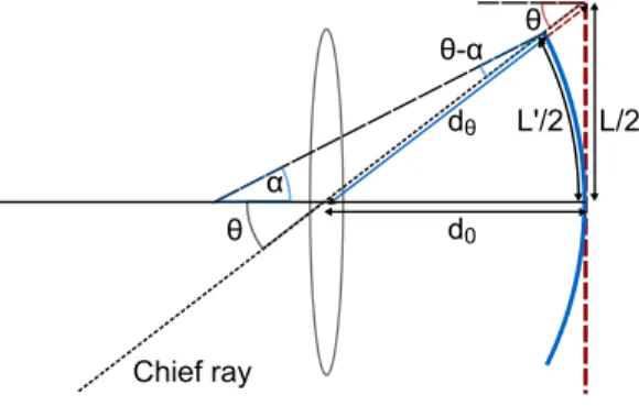
Fig.2 shows the geometry between a spherical concave curved sensor and a lens. Three important changes are presented: the new angle of incidence, θ − α, the reduced distance between the exit
pupil and the image point from dθ = d0/cosθ to dθ = (d0− sag)/cosθ and the reduced size
of the sensor L’ for a same field of view (FoV). sag is the sagitta of the circular arc, and L’ is also the path length of the curve. These modifications improve the illumination by changing the Lambert cosine law in E ~ cos(θ − α) and the inverse square law. Moreover, pixel vignetting decreases with this reduced angle of incidence.
θ θ α θ-α Chief ray d0 dθ L'/2 L/2
Fig. 2. Primary differences between curved and flat sensor for thin lens.
The FoV = 2θ is also improved, calculated with the chord of the sensor, the focal length f, the
sagitta of the sensor and the radius of curvature R of the circular arc such as:
FoV = 2arctan( Rsin(α)
f − R(1 − cos(α))) ≈ 2arctan(
L0
2( f − L8R02)
) (1)
The second equation is for small angles α at the second order. For convex sensors, the new geometry gives same relations, by changing sign of α and sag, slightly degrading illumination and FoV. Finally, this section presents changes with the new geometry of curved sensors. During the design of optical systems with curved sensors, all these changes have to be taken into account.
3.2. Evolution of the curvature for large range of distance
According to Welford [20], two primary aberrations, astigmatism (SI I I) and Petzval curvature
(SIV) in term of Seidel aberration, have to be taken into account to obtain the best image curved
surface. In this case, the best spherical image surface is the surface containing disc of least confusion, which has a curvature c:
c= −n(2SI I I+ SIV)
H2 (2)
nis the index of the media, H the Lagrange invariant. We choose to investigate the change of this
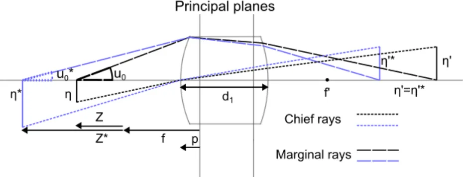
curvature with the distance of the scene on a single lens with an aperture stop at the first surface. Using the principal planes representation of the Fig.3, the slope of the marginal ray is :
u0=
−h1
z+ f − p (3)
where z is the distance from the focal plane to the scene, f is the focal length, p is the distance from the principal plane to the first surface. Seidel aberrations are the sum of the Seidel surface
u0* u0 η* η Marginal rays Chief rays η' η'* f Z* Z f' η'=η'* p d1 Principal planes
Fig. 3. Image of the scene at different positions, Z∗and Z. The size of the image η0is the same, giving two sizes for the object.
coefficients (S3i, S4i) calculated for each surface i with the height hi and the slope ui of the
marginal ray and the chief ray ( ¯ui and ¯hi). We have for these rays (the product has a decreasing
increment j): © « hi+1 niui ª ® ¬ = x i Ö j=1 © « 1 −Kjdj nj dj nj −Kj 1 ª ® ¬ © « h1 n0u0 ª ® ¬ (4)
dj the thickness, nj the refraction index between the surface j and j+ 1, the power Kjof the
surface j . Using expressions of S3i, S4i from Welford [20], we developed SI I I in function of u0
and H:
SI I I = S31+ S32= H2cI I I(u0)= H2(a0+ a1u0+ a2u20) (5)
cI I I(u0) is here corresponding to the curvature of the sagittal focal surface curvature when SIV
is zero. a0, a1and a2are constants depending of values of power, refraction index and thickness
of the lens. Specific values of lens surface curvature can help for constant image curvature. For
example, a2 = 0 when c2 = −d11 or c2 = −nd11+1n1 or d1 = 0 with c2the curvature of the second
surface of the lens. Considering the Petzval sum P, independent of distance, we have for n=1 and z , 0: c(u0)= − n(2SI I I + SIV) H2 = −2a0− P − 2a1u0− 2a2u 2 0 (6)
These calculations can be extended for all systems. Finally, the curvature of the surface containing
the disc of least confusion varies as a second degree polynomial equation according to u0. These
relations can be used to analyze the evolution of the surface curvature for systems with a large range of working distances.
4. Optical designs: fisheye zoom camera and compact architecture
In this section, we present the developments of a wide field zoom design [21] and a compact architecture optimized with our next methodology. We choose to design optical systems at
infinite conjugate. The sensor takes into consideration σ1max1<200 Mpa for its curvature. The
incident angle is controlled to be nearly the same as commercial designs.
4.1. Fisheye zoom system
4.1.1. Methodology during the design process
The starting point is a commercial zoom fisheye camera of 180◦ FoV at F/4 (Canon 8-15
mm [22]). The goal is to keep the exact same main characteristics (back focal distance, field of view, F-number) while reducing the number of lenses and improving the performance. During the
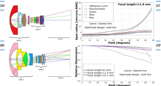
optimization process, we have simplified the optical system by suppressing field-flattening lenses one by one and re-optimizing at each step. In such a wide field system, some field-flattening lenses used closed to the focal plane have a positive power. This removal process is complex since the suppression of one lens strongly modifies the optical characteristics and increases the aberrations, creating a positive-curved field of curvature. Also, we have decided to maintain a fixed curvature over the zoom range due to manufacturing considerations. While the Canon objective is made of 14 lenses, 10 materials and an aspherical surface, the ultimate configuration we have achieved is made of 11 spherical lenses (no aspherical surface) and 7 glass materials, for an improved performance on sharpness and mechanical vignetting.
Focal length=8.1mm Focal length=11.9 mm Focal length=15.1 mm 0 10 20 30 40 50 60 70 80 90 0 10 20 30 40 50 60 70 80 90 Field [degrees] Field [degrees] 0.0 0.2 0.4 0.6 0.8 1.0 0 5 10 15 20 25 30 Red Blue Green Polychromatic Diffraction Limit Relative Illum ination Spot radius [microns R MS] Focal length=11.9 mm
Canon: Dashed line Optimized design: solid line
Canon: Dashed line Optimized design: solid line
Fig. 4. a) Optical layouts of the Canon objective; b) Simplified zoom camera NB: The color code for glass materials is different for each system; Comparison between Canon and simplified design on c) RMS spot radius and d) relative illumination.
4.1.2. Optical performance
To compare the performance of this design and the Canon design, we quantified on Fig.4 the spot size at the focal length of 11.9mm and the relative illumination for three focal length values: 8.1, 11.9 and 15.1 mm. The relative illumination curve is used to quantify changes in the illumination level across the field. The performance improvement is significant. At a focal length of 11.9 mm, the spot radius is close to the diffraction limit and very homogeneous over the field with a gain off-axis up to a factor 5 compared to the Canon. The mechanical vignetting is fully suppressed while it drops down by 30-50% for the Canon objective at the edge of the field of view, improving the relative illumination. The contrast has also globally been improved by a factor 2.5 and the lateral chromatic aberration reduced by a factor 2.
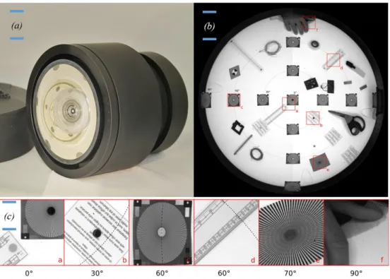
We realized a prototype of this design as well as the curving of a 20 Megapixels front-side illuminated 24x32 mm CMOS sensor (CMOSIS CMV20000), used in a commercial packaging. The sensor is convex with a radius of 280mm. No significant differences on the electro-optical response have been observed [16]. Fig.5 shows the integrated objective and an image acquisition with good performances, sharpness and contrast, over the full field of view. It has been taken at full aperture F/4. We can also note that there is no drop of illumination off-axis, enabling well
Fig. 5. a) Simplified zoom prototype; b) Image acquisition at 8 mm focal length F/4 of an object located at 400 mm from the objective in all direction; c) zoomed parts of image acquisition.
4.2. Compact wide angle camera
4.2.1. Methodology during the design process
The starting point is the monocentric lens, studied in recent publication [2]. This system theoretically presents wide field of view, compactness, high resolution and the sensor is curved on the Petzval Surface. The field of view, which is the subtended angle of the sensor, drops
to at most 17 degrees at any sensor’s size using mechanical limits σ1max1=200 MPa, Fig 1.
The goal is to keep high resolution and compactness and increase the field of view. During the optimization process, new spherical lenses are added in order to decrease step by step the subtended angle of the sensor. The final version of this new architecture, showed Fig 6, has 6 spherical lenses, with the first cemented triplet and two lenses with a positive optical power, and the last one with a negative power. An important characteristic is the position of the aperture stop which is at the start of the design. This combination of lenses is only adapted with the use of curved sensor, because of the large amount of field curvature aberration in the system which cannot be reduced without the addition of new lenses and the degradation of the sharpness. Finally, the field of view is 40 degrees compared to 8 degrees of subtended angle of the sensor.
4.2.2. Optical performance
We show on Fig.6 the Modulation Transfer Function (MTF) of the system at F/2.6 and a maximum field of 4.40mm. We compare it with an equivalent commercial system, with nearly the same characteristics as the size of the sensor, the focal length and the image quality. The MTF of both systems are similar for a field range close to zero, but at edges our system shows better values of
performances. We realized a prototype of this camera using the curving process on a commercial
Fig. 6. a) Optical layout of the compact system; b) MTF comparison over the field.
product 1/1.8” format 1.3Mpx global shutter CMOS sensor (Teledyne EV76C560). The system with a curved sensor shows a large gain in compactness, more than a factor of two compared to its equivalent commercial system. The commercial objective offers an adjustable iris whereas it is not the case for the prototype lens since the main goal is to demonstrate the gain on the optical compactness while providing better performance. Also, straylight issues has been addressed by designing an additional hood to prevent out-of-field straylight (not shown in Fig.7 a). Preliminary images have been realized, as shown in Fig.7.
(a) (b) (c) Commercial objective Compact prototype
Fig. 7. a) Comparison between integrated prototype and commercial objective; b) Compact objective; c) First image of the compact optical architecture system in RAW data at 40 cm of working distance.
5. Conclusions
In this paper, we have discussed new considerations for the design of enhanced performance optical systems with curved sensors. First, we have presented FEA developments on the sensor curvature, providing bending mechanical limits. Second, we have shown that the curved image surface changes the geometry of optical systems, giving new relations of illumination and field of view. Seidel aberrations have been discussed and we demonstrated conjugate relations for macro lenses applications. Third, two designs have been realized by using the two previous points in
field of view with a convex curved sensor. We have improved the performance of sharpness and reduced the mechanical vignetting. An adding process is described to design a compact camera from a monocentric lens. Keeping the same optical characteristics, the field of view may also be multiplied by five. Finally we have realized two complementary prototypes, confirming all the advantages of using a curved sensor over a large range of field of view. We believe that the development of curved sensors offers new possibilities in the design of optical systems for numerous applications from miniaturized devices to large scale systems.
Acknowledgements
This activity was partially funded by the French Research Agency (ANR) through the LabEx FOCUS ANR11LABX0013, and will be pursued in the frame of the H2020 ERCSTG2015 -678777 ICARUS program over the period 2016-2021.
References
1. S. B. Rim, P. B. Catrysse, R. Dinyari, K. Huang, and P. Peumans, "The optical advantages of curved focal plane arrays," Opt. Express 16(7), 4965-4971 (2008).
2. I. Stamenov, A. Arianpour, S. J. Olivas, I. P. Agurok, A. R. Johnson, R. A. Stack, R. L. Morrison, and J. E. Ford, "Panoramic monocentric imaging using fiber-coupled focal planes," Opt. Express 22(26), 31708-31721 (2014). 3. O. Iwert and B. Delabre, "The challenge of highly curved monolithic imaging detectors," Proc. SPIE 7742,774227
(2010).
4. E. Muslimov, E. Hugot, W. Jahn, S. Vives, M. Ferrari, B. Chambion, D. Henry, and C. Gaschet, "Combining Freeform Optics and Curved Detectors for Wide Field Imaging: A Polynomial Approach over Squared Aperture," Opt. Express 25, 14598-14610 (2017).
5. D. Reshidko, and J. Sasian, "Optical Analysis of Miniature Lenses with Curved Imaging Surfaces," Appl. Opt. 54, E216-E223 (2015).
6. H. C. Ko, M. P. Stoykovich, J. Song, V. Malyarchuk, W. M. Choi, C. J. Yu, J. B. Geddes 3rd, J. Xiao, S. Wang, Y. Huang, and J. A. Rogers, "A hemispherical electronic eye camera based on compressible silicon optoelectronics," Nature 454(7205), 748-753 (2008).
7. X. Xu, M. Davanco, X. Qi, and S. R. Forrest, "Direct transfer patterning on three dimensionally deformed surfaces at micrometer resolutions and its application to hemispherical focal plane detector arrays," Org. Electron. 9(6), 1122-1127 (2008).
8. I. Jung, G. Shin, V. Malyarchuk, J. S. Ha, and J. A. Rogers, "Paraboloid electronic eye cameras using deformable arrays of photodetectors in hexagonal mesh layouts," App. Phys. Lett. 96 (2), 021110 (2010).
9. Y. M. Song, Y. Xie, V. Malyarchuk, J. Xiao, I. Jung, K. J. Choi, Z. Liu, H. Park, C. Lu, R. H. Kim, R. Li, K. B. Crozier, Y. Huang, and J. A. Rogers, "Digital cameras with designs inspired by the arthropod eye," Nature 497(7447), 95-99 (2013).
10. T. Wu, S. S. Hamann, A. Ceballos, O. Solgaard, and R. T. Howe, "Design and fabrication of curved silicon image planes for miniature monocentric imagers," in 2015 18th International Conference on Solid-State Sensors, Actuators and Microsystems, TRANSDUCERS 2015 (2015), pp. 2073-2076.
11. R. Dinyari, S. B. Rim, K. Huang, P. B. Catrysse, and P. Peumans, "Curving monolithic silicon for nonplanar focal plane array applications," Appl. Phys. Lett. 92(9), 091114 (2008).
12. K. Itonaga, T. Arimura, K. Matsumoto, G. Kondo, K. Terahata, S. Makimoto, M. Baba, Y. Honda, S. Bori, T. Kai, K. Kasahara, M. Nagano, M. Kimura, Y. Kinoshita, E. Kishida, T. Baba, S. Baba, Y. Nomura, N. Tanabe, N. Kimizuka, Y. Matoba, T. Takachi, E. Takagi, T. Haruta, N. Ikebe, K. Matsuda, T. Niimi, T. Ezaki, and T. Hirayama, "A novel curved CMOS image sensor integrated with imaging system," Digest of Technical Papers - Symposium on VLSI Technology, 6894341 (2014).
13. B. Guenter, N. Joshi, R. Stoakley, A. Keefe, K. Geary, R. Freeman, J. Hundley, P. Patterson, D. Hammon, G. Herrera, E. Sherman, A. Nowak, R. Schubert, P. Brewer, L. Yang, R. Mott and G Mcknight, "Highly Curved Image Sensors: A Practical Approach for Improved Optical Performance." Optics Express 25(12), 13010 (2017).
14. K. Tekaya, M. Fendler, K. Inal, E. Massoni, and H. Ribot, "Mechanical behavior of flexible silicon devices curved in spherical configurations," in 2013 14th International Conference on Thermal, Mechanical and Multi- Physics Simulation and Experiments in Microelectronics and Microsystems (EuroSimE, 2013), paper 6529978.
15. D. Dumas, M. Fendler, N Baier, J. Primot, and E. Le Coarer, "Curved focal plane detector array for wide field cameras," Applied Optics 51(22), pp. 5419-5424 (2012).
16. B. Chambion, C. Gaschet, T. Behaghel, A. Vandeneynde, S. Caplet, S. Gétin, D. Henry, E. Hugot, W. Jahn, S. Lombardo, M. Ferrari, "Curved sensors for compact high-resolution wide-field designs: prototype demonstration and optical characterization", Proc. SPIE 10539, 1053913 (2018).
17. B. Chambion, L. Nikitushkina, Y. Gaeremynck and W. Jahn, "Tunable curvature of large visible CMOS image sensors: Towards new optical functions and system miniaturization," IEEE ECTC 178-187 (2016).
18. W. Jahn, M. Ferrari, E. Hugot, B. Chambion, G. Moulin, L. Nikitushkina, C. Gaschet, D. Henry, S. Getin, and Y. Gaereminck, âĂIJFlexible focal plane arrays for UVOIR wide field instrumentation,âĂİ Proc. SPIE 10562, 105624Z (2016).
19. J.-H. Zhao, J. Tellkamp, V. Gupta and D. R. Edwards, "Experimental evaluations of the strength of silicon die by 3-point-bend versus ball-on-ring tests", IEEE Trans. Electron. Packag. Manuf., vol.32(4), pp.248-255 (2009). 20. WT. Welford, Aberrations of Optical Systems (Taylor and Francis, 1986).
21. W. Jahn, Laboratoire d’Astrophysique de Marseille, Aix Marseille University, 58 Blvd Charles Livon 13284 Marseille, France, is going to publish a PhD thesis entitled "Innovative focal plane design for high resolution and Earth observation: Freeform optics and curved sensors"