Design and Testing of a Gated Electron Mirror by
John Simonaitis B.S. Electrical Engineering
University of Illinois at Urbana-Champaign (2018)
Submitted to the Department of Electrical Engineering and Computer Science in Partial Fulfillment of the Requirements for the Degree of
Master of Science in Electrical Engineering and Computer Science at the
MASSACHUSETTS INSTITUTE OF TECHNOLOGY February 2021
©Massachusetts Institute of Technology. All rights reserved.
Signature of Author: . . . . Department of Electrical Engineering and Computer Science
January 15, 2020
Certified by . . . . Karl K. Berggren Professor of Electrical Engineering and Computer Science Thesis Supervisor
Certified by . . . . Phillip D. Keathley Group Leader, Research Laboratory of Electronics Thesis Supervisor
Accepted by . . . . Leslie A. Kolodziejski Professor of Electrical Engineering and Computer Science Chair, Department Committee on Graduate Students
High Voltage, Vacuum Integrated Electronics for Nanosecond Switched Charged Particle Optics by
John Simonaitis
Submitted to the Department of Electrical Engineering and Computer Science on January 31, 2021 in Partial Fulfillment of the Requirements for the Degree of
Master of Science in Electrical Engineering and Computer Science
ABSTRACT
One of the primary limiting factors of modern electron microscopes is the damage imparted to samples during imaging, which limits the achievable image resolution for many biological specimens [1]. Recently, there have been several microscope designs proposed to improve resolution in these samples by reduc-ing beam damage employreduc-ing novel quantum measurement schemes such as interaction free measurement [2] and multi-pass electron microscopy [3]. These designs fall under the heading of a quantum electron microscope (QEM). A recurring element of all actively explored QEM designs is a linear cavity for recircu-lating electrons. This cavity, which could be inserted into existing microscopes, would allow for either the wavefunction transfer required for interaction free measurement or the phase build-up needed for multi-passing protocols to reduce specimen damage. In order to achieve these modes, there must be some way to open and close this cavity in a controlled fashion to allow electrons to enter, stably recirculate, then exit the setup. One approach to realizing such a cavity is the construction of a gated electron mirror, an electron optical element capable of switching between two operating states. In one state it transmits elec-trons travelling along its optical axis, while in the other it reflects them back onto their incident path. This gated mirror is required to operate at kilovolt potentials and reflect electrons with high accuracy within a several-nanosecond switching time frame.
In this thesis, we aim to develop, build, and test such a gated electron mirror. We first outline in Chap-ter 1 the electron-damage problem, approaches to solving it, and how QEM might do this. Next, in ChapChap-ter 2, we review state-of the art fast pulsing approaches, as well as requirements for the mirror. In Chapter 3 we then design and test a fast pulse generating circuit based on emerging Gallium Nitride on silicon technology. In Chapter 4 we simulate the performance of the gated mirror. We optimize the structure of the gated mirror to minimize transition times and errors, and avoid induced voltage changes in other parts of the apparatus. We also discuss various design approaches to improve device performance, such as integrating high voltage pulsing electronics into the gated mirror itself. We also discuss the ultimate limits of switching. In Chapter 5 we then develop and show progress on an apparatus for testing the switching characteristics of the gated mirror in both time and frequency domains, directly probing the changing fields using an electron beam. Finally, in Chapter 6 we discuss improvements to our measurements and next steps.
Thesis Supervisor: Karl K. Berggren
Title: Professor of Electrical Engineering and Computer Science Thesis Supervisor: Phillip D. Keathley
Acknowledgments
This work would not have been possible without the constant help and advice from many of my friends, family, colleagues, and mentors. In particular, I would like to thank the following people who have helped me the above and beyond:
My co-advisors Prof. Karl K. Berggren and Dr. Phillip D. Keathley, for their constant mentorship and for creating a exciting and deeply collaborative research environment to work in. In addition, I would like to thank Karl for his excitement for the little victories in research, his emphasis on the broader responsibilities of his students as citizens and scientists, and his open acceptance of both crazy ideas and failure. I would also like to thank Donnie for the many great conversations we have had about engineering and science in general, for his tireless hands-on help with the practical aspects of research, and most of all for helping me understand difficult problems when I asked for help, and especially when I did not. I have learned so much from both of you, in research and outside of it.
I would also like to thank Dr. Yugu Yang-Keathley and Ben Slayton for the tremendous help you both gave with simulating and understanding gated mirrors, the core work of this thesis.
In addition, I would like to thank Dr. Akshay Agarwal, Navid Abedzadeh, Marco Turchetti, and Peter Satterthwaite for many great conversations in research and beyond. I would also like to thank everyone in the QNN group for creating such an open and fun research environment.
I would like to thank our collaborators in the QEMII Collaboration for many extremely useful con-versations and for laying the groundwork for this thesis. I would like to specifically thank the Kasevich group at Stanford, especially Adam Bowman, Brannon Klopfer, and Stewart Koppell, for many discussions of the gated mirror and electronics to drive it, and Prof. Pieter Kruit and Maurice Krielaart at TU Delft for incredibly useful discussions on constructing a gated mirror and streak camera.
I thank Gordon and Betty Moore Foundation for supporting the Quantum Electron Microscope project, and the National Science Foundation for supporting my studies. This material is based upon work sup-ported by the National Science Foundation Graduate Research Fellowship under Grant No. 1745302.
I would last like to thank my parents, Bill and Kathleen Simonaitis, for fostering my curiosity in every-thing, even if it meant me taking apart televisions and microwaves and scattering the remains about the basement. I’d like to thank my brothers, Pat and Will, for putting up with the know-it-all-ism that likely led me on the path to graduate school. Lastly, I’d like to thank my grandparents, George Cady, Kathleen Cady, Grace Simonaitis, and Dr. John Simonaitis for teaching me so many lessons in life, from how to treat others to living life with endless curiosity.
List of Figures
1.1 Various Damage Mechanisms in Electron Microscopy . . . 11
1.2 Dose-Limited Resolution in Cryo-EM . . . 12
1.3 IFM Demon station . . . 14
1.4 Quantum Zeno Effect Demonstration . . . 14
1.5 Charged Particle Trap IFM . . . 15
1.6 Linear Cavity IFM . . . 16
1.7 Multi-pass transmission electron microscopy enhancement . . . 18
1.8 Multi-pass transmission electron microscopy demonstration . . . 18
2.1 Timing requirements of a gated electron mirror . . . 22
2.2 Approaches to precision high frequency driving . . . 25
3.1 Single-Sided GaNFET Circuit Diagram . . . 29
3.2 GaNFET Circuit Schematic and Layout . . . 31
3.3 Physical GaNFET circuit . . . 32
3.4 GaNFET Circuit Probing . . . 33
3.5 Directly Coupled GaNFET Circuit . . . 34
3.6 Measurement Circuit Models . . . 34
3.7 Oscilloscope Impedance Changes . . . 35
3.8 Ringing in the Directly Connected GaNFET . . . 36
3.9 Bootstrapped GaNFET Circuit Operation . . . 38
3.10 Bootstrapped GaNFET Circuit Design . . . 39
3.11 Bootstrapped GaNFET Results . . . 40
3.12 Assembly of Circuit . . . 41
4.1 Representation of the GaNFET Simulation . . . 46
4.2 Simulation of a Gated Mirror Load . . . 48
4.3 Fourier Calculations . . . 50
4.4 Simulated Gated Mirror Response . . . 51
4.5 Field Sampling Points in the Gated Mirror Spatially . . . 53
4.6 Ground Bounce . . . 54
4.7 Comparison of Gaussian Switching . . . 56
4.8 Gated Mirror Modes Overview . . . 56
4.9 Different Modes in the Gated Mirror . . . 58
4.10 Normalized Mode Development in the Gated Mirror versus Frequency . . . 59
4.11 Einzel Lens Simulation . . . 60
4.12 Einzel Lens . . . 62
4.13 Inductive Topology . . . 62
5.1 Electron Paths in the Gated Mirror . . . 67
5.2 Optimized Gated Mirror . . . 68
5.3 Optimized Gated Mirror Fabrication . . . 69
5.4 Streak Camera Operation . . . 70
5.5 Streak Camera Implementation . . . 71
5.6 Streak Camera Electronics . . . 72
5.7 Imaging of a Gated Electron Mirror in an SEM . . . 73
Contents
1 Mitigation of Radiation Damage by Quantum Electron Microscopy 10
1.1 Existing approaches to improving dose-limited resolution . . . 10
1.2 Quantum approaches . . . 12
1.2.1 Structured Illumination and Entangled States . . . 13
1.2.2 Interaction free measurement . . . 13
1.2.3 Multi-pass electron microscopy . . . 17
2 Requirements for Pulsing of a Gated Electron Mirror 20 2.1 Requirements for a gated electron mirror . . . 20
2.2 Approaches to Fast Pulsing . . . 23
3 Design of Gallium Nitride High Voltage Pulsers 28 3.1 Single-Sided Circuit Design . . . 29
3.2 Circuit Testing . . . 32
3.3 Double-Sided Pulsing . . . 37
3.4 Assembly Procedure . . . 40
3.5 Circuit Testing Procedure and Safety . . . 43
4 Simulation of Pulser Switching Performance in Real Loads 45 4.1 Integrated Simulations of a Gated Mirror . . . 45
4.2 Analysis of Mode Structure and Aberrations . . . 51
4.2.1 Maximum Switching Speeds and Voltages . . . 54
4.3 Analysis of Other Loads . . . 60
5 Testing of the Gated Electron Mirror 66 5.1 Calculation of Observable Outputs . . . 66
5.2 Construction of a Gated Mirror . . . 67
5.3 Designs for a Streak Camera . . . 69
5.3.1 Early Results . . . 72
6 Conclusions and Future Work 75 6.1 Improvements to Simulation Resolution Near the Optical Axis . . . 76
6.2 Electron Interactions with the Gated Mirror . . . 76
6.3 Frequency Domain Streak Camera Improvements . . . 77
Chapter 1
Mitigation of Radiation Damage by
Quantum Electron Microscopy
One of the key challenges of modern electron microscopy is the imaging of beam sensitive specimens. While inorganic materials such as carbon and gold can be imaged directly to sub-Angstrom atomic resolu-tion, organic samples such as proteins and viruses can not due to the immense amount of damage caused by incident electrons [4]. Modern transmission electron microscopes (TEMs) are limited in their resolution by the the maximum number of electrons that can be used to image a sample before it is destroyed, and the smallest length scale of a specimen they can resolve is referred to as their dose-limited resolution [4, 5].
In this chapter, we first briefly review the state of the art in the electron microscopy of biological specimens, as well as routes for improving these and the ultimate limits of cryo-EM. Then, we explore the possibility of quantum techniques, which are aimed at using quantum resources (electrons) as efficiently as possible to obtain the best possible signal-to-noise ratios in our specimen with the least damage. This lower damage leads to the best possible resolution. Finally, we discuss our general efforts to develop one of these schemes for quantum electron microscopy (QEM), outlining each required component [2]. This thesis focuses on the development of one of the central components of such an instrument, a gated electron mirror.
1.1
Existing approaches to improving dose-limited resolution
An understanding of damage in cryo-EM is crucial to understanding approaches to mitigating it, as well as the inherent resolution limitations caused by it. Damage in cryo-EM stems from two types of elec-tron scattering: elastic scattering of high-energy elecelec-trons from the nucleus, which can cause ejection of
Figure 1.1: (a) Elastically scattered electrons, with the outer incident electron showing scattering that leads to image contrast, and the inner strongly scattered electron showing knock-on damage, where the backscattering of the electron leads to ejection of the atom. (b) Inelastically scattered core-shell electron scattering, where an inner electron is ejected from the atom to a higher valence state. Upon the return of this electron to the ground state, x-rays are generated. (c) Inelastically scattered valence-shell electron scattering. This kind of electron-electron scattering leads to irreversible damage through bond breaking and heating of the material of interest. Figure taken from Fig. 1.1 of R.F. Egerton [5]
atoms from a material, and inelastic electron-electron scattering, which causes charging, heating, struc-tural deformation, and mass loss in samples due to disruption of electron bonds in materials [5]. This is demonstrated in Fig. 1.1 taken from Chapter 1 of [5]. These unavoidable damage processes significantly limit resolution in beam sensitive specimens to a few nanometers, far larger than the sub-Angstrom capa-bilities of aberration-corrected TEMs [6]. An example of this can be seen in Fig. 1.2, where at low doses the resolution is limited by noise in the system, and at high doses the resolution is limited by damage to the specimen.
A major breakthrough in the imaging of biological specimens was the development of electron cryo-microscopy (cryo-EM) [7, 8, 9], which netted its inventors the 2017 Nobel Prize in Chemistry. This tech-nique, which works by freezing molecules in vitreous ice, destructively imaging millions of copies them to get partial information from each, and then reconstructing this information into a three-dimensional representation of the molecule, only achieved atomic resolution in 2020 [10]. Even still, there are many shortcomings of this approach such as its ability to only image large proteins and the requirement of imaging millions of copies of the specimen, which takes significant time and computational resources, and destroys the possibility of real-time imaging of structural changes [11, 12].
Many approaches have been taken and proposed to improve Cryo-EM performance further through purely classical means. Examples offering substantial improvement include: cooling and encapsulating of specimens to reduce heating and protect from mass loss [4]; optimization of incident beam energy and specimen thickness [14, 13]; improvements to the energy spread and coherence of electron sources [15];
Figure 1.2: Example of dose-limited resolution in cryo-EM. At low doses, resolution is limited by shot noise, while at higher doses the damage limits resolution. This figure shows the effect of changing specimen thickness on damage. Figure taken from [13].
improvements in detector quantum efficiencies to waste as few electrons as possible[16]; and improve-ments to computational reconstruction algorithms [17].
One important aspect to minimizing damage and producing high quality images in cryo-EM is under-standing contrast mechanisms in it. All organic molecules are made primarily of light elements such as carbon and hydrogen, and thus under electron illumination they appear as weak electron phase objects. In fact, the negligible amplitude blocking they cause is due to damaging events, and thus is optimally avoided. Therefore, in perfect focus it is impossible to form an image of proteins with significant contrast. The historical way of getting around this in Cryo-EM was to instead defocus the probe slightly, using the so-called Scherzer defocus [18]. Only since 2001 have components such as the Zernike [19, 20], Volta [11], and Boersch [21] phase plates enabled direct phase contrast of specimens. Since 2016, various propos-als and demonstrations have emerged that aim to improve these phases further by adapting them in-situ. [22, 23]. However this adaptive approach is still in its infancy.
1.2
Quantum approaches
In recent years, much work has been proposed to take advantage of the quantum nature of electrons in biological imaging. This work seeks to use electron properties such as their phase, wavelength, and wave-front structure as an advantage in quantum sensing, rather than a detrimental trait that limits resolution and makes contrast generation more difficult. A few of these approaches are reviewed below, before dis-cussing the approach that is the subject of this thesis.
1.2.1 Structured Illumination and Entangled States
One proposal to improve resolution in Cryo-EM is through the use of structured illumination. Structured illumination has already been demonstrated to some degree through the generation of electron vortex beams [24, 25], useful states for imaging the magnetic properties of materials. General structured illumi-nation takes this several steps further. The basic idea of this is to use patterned or adaptive phase plates to impart complex structure onto the electron probe. This structure is tailored to a specific protein, and if the protein is illuminated properly, the resulting wave function scattering leads to the refocusing of the beam to a distinct point in space [26]. If any other protein is illuminated, the electron will scatter off to com-pletely different locations. The core appeal of this approach is that it might be possible to identify and sort proteins using only a single electron. However challenges in realizing such adaptable phase plates and ac-counting for the many possible orientations of proteins in vitreous ice can be in have yet to be settled. This work was recently funded by the European Union’s Horizon 2020 Research and Innovation Programme under Grant Agreement No 766970 Q-SORT (H2020-FETOPEN-1-2016-2017), and is an exciting quantum approach to protein imaging.
Another proposal that seeks to reduce electron damage in Cryo-EM uses entanglement to improve image signal-to-noise ratios to the quantum limit [27, 28, 29]. This concept is similar to the use of N00N states in light optics to reduce the quantum resources required for a given measurement accuracy [30]. The idea is that by entangling incident electrons with quantum resources such as flux or charge qubits, we can reduce shot noise scaling as a function of particles used N past the classical limit of 1/√N and to the quantum limit of 1/N. However, this approach has numerous technical challenges and has yet to be realized.
1.2.2 Interaction free measurement
Another approach to reducing electron beam damage stems from the famous thought experiment of Elitzur and Vaidman [31] known as interaction free measurement (IFM). The core idea of this is summarized in Fig. 1.3 below, where the object is taken to be a ”quantum bomb” for dramatic effect. If an object exists in the path, there is a 25% chance of measuring its existence without interacting with it, as described in 1.3. While interesting, this is not particularly useful.
This thought experiment was later extended in the work of Kwiat et al. [32] to result in the detection of an object with zero chance of interacting with it. This is achieved through the principle or repeated interrogations, or the quantum Zeno effect, shown in Fig. 1.4. By probing the sample with only a tiny
Figure 1.3: IFM Demonstration. The dotted circle represents where an object would be placed in this experiment. Starting from the bottom left we have an incoming quantum resource. This is the split into a 50-50 chance of either path at the beam splitter (the diagonal dotted line). This is then recombined at the second beam splitter in the top right. In the case of no object then we can vary the relative phase to interfere the electron with itself to constructively interfere at D1and destructively interfere at D2, always leading to a D1count. If we then put an absorptive object in this path as shown, suddenly this interference can not occur. In this case there is a 50% chance of hitting the object and a 50% chance of hitting the second beam splitter, leading to a 25% chance of hitting D1 and a 25% chance of hitting D2. In this case, hitting
D2implies an object was in the path, but there if it hit D2it could not have interacted with the object, and so we can infer its existence without an interaction. This is the crux of IFM. Figure taken from [31]
probability many times, the overall probability of interaction approaches zero, while the probability of detecting the object if it exists approaches one. The difference between no object and an object is illustrated in 1.4a and 1.4b respectively. In case (a), the electron simply resonates to the top half through a partial mirror of reflectivity 1/N over N iterations, eventually entering the top. In case (b), the electron repeatably interrogates the sample, with a probability of interacting of 1/N2 on each pass. The total probability of interacting is then just 1/N. As N approaches infinity, the interaction probability approaches zero, and the measurement truly becomes interaction free.
Figure 1.4: Quantum Zeno Effect Demonstration. (a) Repeated splitting of the electron wavefunction leads to the coherent transfer of the electron from the lower half of the figure to the upper half. (b) Repeated splitting of the electron wavefunction with an object blocking coherent transfer to the upper half. Figure taken from [32]
Figure 1.5: A proposed IFM experiment using charged particle traps. (a) The experimental setup, where two closely spaced charge particle traps form an effective potential Uef fwith states |T and |B corresponding
to a particle in the top and bottom well respectively. (b) The proposed interaction free measurement, where in each circulation of the top loop there is some electron wavefunction coupled into the bottom. Figure taken from [33]
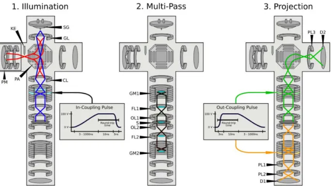
In 2009, Putnam and Yanik proposed an experimental realization of this concept using electrons held in charged particle traps [33]. This worked by forming a double well potential as shown in Fig. 1.5a. In this experiment, the electron circulates inside the trap, and after each round trip some of the electron is coupled into the bottom loop. which is shown in Fig. 1.5a. In the case of the black pixel, this transfer is disrupted each circuit of the loop, interacting slightly with the black pixel and keeping the electron in the upper loop. In the white pixel, no blockage occurs and the wavefunction is fully transferred from the top to the bottom state. By tuning the number of round trips N needed to fully switch from one trap to the other (and therefore the coupling strength), this could theoretically achieve IFM measurements with the damage probability approaching zero, limited only by the coherence time of the electrons in the circulator. In 2016, designs for the realization of an IFM scheme in an electron microscope were proposed by Kruit et al. [2]. This approach introduced several new elements to a standard TEM, the most notable being a pulsed electron source, a recirculating cavity, gated electron mirrors to in-couple and out-couple electrons, and a coherent beam splitting element. These elements are summarized in Fig. 1.6 from the work of Turchetti et al. [34], where a more specific IFM-based design was proposed.
Figure 1.6: A proposed IFM experiment using a linear cavity in a TEM. (a) A schematic design showing each component of the microscope as described in the text. (b) A ray-optical view of the cavity, showing the various images formed and diffracted orders. (c) A rendering of the gated electron mirror, showing its behavior in the open and closed states. (d) the operation of a related diffractive electron mirror required for successful operation of the cavity. Figure taken from [34].
In this design, shown schematically in Fig. 1.6a, electrons are generated by a laser triggered electron gun before being focused by illumination optics onto the center of the so-called gated electron mirror. When this mirror is in its transmitting state, the electrons pass through, where they impinge on the beam-splitting element, a so-called diffractive electron mirror. Upon reflecting, one of the diffractive orders is incident on the sample, which blocks coherent coupling to that order. After a predetermined number of round trips N set by the coupling strength of the diffractive mirror, the electron is out-coupled to imaging optics and a detector via a second gated electron mirror. If an object exists, the diffraction is blocked and we have most of the intensity in the central order as shown with the opaque pixel. If there is no object, the intensity shifts primarily to the diffractive order as shown in the transparent pixel case. It is critical to have a low-loss or loss-free diffractive element to achieve this, or else the quantum advantage disappears [2].
One of the key elements we highlight is the gated electron mirror, which is crucial for properly in-coupling and out-in-coupling electrons from the cavity. This will be discussed later in this thesis. Another is the diffractive electronic mirror [35] which is based on reflecting electrons from just above a nanostruc-tured surface. While appealing in theory, this has yet to be demonstrated in a modern microscope system, though mentions of this by Lichte et al. from 1983 appear in conference proceedings [36]. Due to the complexity of such a component and its integration into apparatus, our efforts have shifted to focusing on an alternative microscope configuration known as a multi-pass transmission electron microscopy [37].
1.2.3 Multi-pass electron microscopy
The theory of multi-pass transmission electron microscopy (MPTEM) is quite similar to that of an IFM based microscope. The core principle underlying its operation is the concept that repeated weak phase measurements using the same quantum resource results in an enhancement of signal-to-noise (SNR) ratios in a phase measurement [38]. If we have m passes, this leads to an m-fold SNR enhancement when applied to weak phase objects, include all proteins at high electron energies [37]. An example of this enhancement is shown in Fig. 1.7, where we see over multiple passes an enhancement of SNR at various fixed doses.
The design of the MPTEM is extremely similar to an IFM based microscope. The key difference between them is the lack of an explicit electron beam-splitting component such as a diffractive electron mirror [37], although technically one can interpret the sample itself as the beam-splitting element. A proposed design is outlined in Fig. 1.8, which is taken from [39]. The principle of multi-passing has been demonstrated using photons by Juffmann et al. [3], though has yet to be shown with electron illumination.
Figure 1.7: Simulation of the phase enhancement of multi-pass electron microscopy in a real protein. Figure taken from [37].
Figure 1.8: A proposed MPTEM integrated into a linear cavity in a TEM. It is broken into three operating steps: illumination, multi-passing, and projection. Figure taken from [39]
mirror (GM1) is opened with a few-nanosecond-switched voltage pulse. This allows electrons to enter the chamber. Next, we close GM1. The mirror must fully close by the time the electrons return from reflecting off the second gated mirror (GM2) for multi-passing to occur. Finally, we open GM2, allowing the electron that has built up a phase shift from N passes to exit the chamber and be imaged. In contrast to the IFM-based approach, the only novel electron-optical element required for this to function is the gated electron mirror: the topic of this thesis.
Chapter 2
Requirements for Pulsing of a Gated
Electron Mirror
In order to realize a functioning Quantum Electron Microscope, we require some way of stably in-coupling and out-coupling electrons from an electron cavity. Due to the quantum-coherent nature of this approach to imaging, we require stringent performance specifications on this gated electron mirror transition. In this section, we elaborate on these requirements. We also discuss various state-of-the art pulsers and their potential use in a gated mirror, before settling on a technology that is explored in the rest of this thesis.
2.1
Requirements for a gated electron mirror
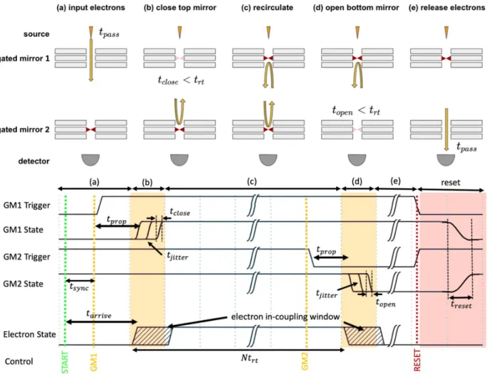
The basic experiment undertaken in both the case of IFM and multi-pass electron microscopy is shown in Fig. 2.1 below. Depending on the microscope design, the gated mirror requirements vary. In this thesis we will discuss the design of a gated mirror for a 10 keV multi-pass based electron microscope [39], but the designs are easily applied to other IFM-based designs as well [34]. There are six operating regimes for the microscope, three static and three transitory. In the first, default, state of the microscope, the top gated mirror is open (held at -9.95 kV), and the bottom is closed (held at -10.05 kV). In this state, electron pulses can be injected into the cavity as shown in Fig. 2.1a. Next, a -100 V pulse is applied to the top Gated Mirror 1 (GM1), putting it in the transitory regime shown in Fig. 2.1b. This transition must be completed in a time tclosewhich is less than the round-trip time of the cavity, trt. Previous work has used classical estimates to show that the mirror must be within 1% its final value in order to minimize spatial and energetic aberrations to the the electron probe [39, 34]. Of course, given that our approach is quantum and requires continued coherence of the electron packet after reflection in all cases, the requirements may be more stringent. This
is discussed in Chapter 4.
Assuming proper shutting of the cavity and stable in-coupling of the electron beam, we allow the electron to recirculate for N round trips, the number N being set by optimizing for the phase accumulation and absorption per pass. This is shown in Fig. 2.1c. Next, we must open the second gated mirror (GM2), again in a time topenless than the round trip time of the cavity, trt. This time, we apply a positive +100 V pulse to GM2. Now that the electron beam no longer has to be re-imaged onto the sample and recirculated stably in the cavity, the requirements for the opening ringing are less stringent. In the final state (Fig. 2.1e) the pulse is simply released onto an imager from the cavity. After this, the pulses can stop being applied, and the system slowly reset to state (a).
Figure 2.1 shows a timing diagram of this process, allowing us to think clearly about the system re-quirements for such a cavity. Each grey dotted line corresponds to a single round trip, or time trt. Each cycle starts when an electron packet is generated by the pulsed source shown by the green START line in Fig. 2.1, which for our purposes we set to a repetition rate of 1 MHz. GM1 Trigger and GM2 Trigger the control signals for the system which start opening and closing GM1 and GM2 respectively. GM1 State and GM2 State are the actual voltages of the mirror, and show the finite transition times of the system tclose and topen. Note that we flip the sign of the plot to show a rising edge as closing, since that corresponds to the energy barrier the negatively charged electron sees. tproprefers to the time between setting the mirror state and it physically changing. This is determined by the delay time from the computer control to the switching circuitry, the propagation time of the switching circuitry, and the propagation time of the high voltage signal to where the electron sees. The term tjitter refers to the total jitter time from the electron generation to the closing of the cavity, and is comprised of uncertainty from the electron generation to clock, signal propagation, and pulse generation. Electron State refers to whether or not the electron is in the recirculating cavity, and is simply there to clarify the cavity operation.
In order to properly in-couple the electron, we must set tsync to equal tarrive− tprop− tjitter, with tjitterset as the threshold for the number of successful in-couplings given unavoidable system jitter. For our purposes we set this so that more than 99% of in-couplings are successful. Depending on the rise time of the switching pulse, we have an in-coupling window given by twindow = trt− tclose− tjitter, where tclose is the closing time to achieve a specified voltage error (in our case less than 1%). The larger this window, the more time we can have to in-couple current to the cavity, and the less reduction we have in overall system current, shown in Eqn. 2.1, where trepis the repetition period of the pulsed source and Igun the standard TEM gun current. This assumes the pulse length is perfectly length twindow. This current estimate neglects concerns for decoherence from space charge effects in the cavity, especially in regions
Figure 2.1: Timing diagram of a gated electron mirror, with the various states and transitions labeled. Each heading (a-e) responds to the 5 stages discussed, along with the resetting state. Each dotted line segment corresponds to a the round trip time of the cavity, trt. (a) The input state, where the top gated mirror GM!
is held open, and GM2 is held closed. (b) The capturing of the electron in the cavity, where the electron reflects off GM2 and we must close GM1 before the electron reaches it in time trt. (c) The recirculating
phase, where the electron loops in the cavity for a predetermined time set by the round trip time and desired number of passes. (d) The releasing phase, where we open GM2 before the electron hits to out-couple the electrons without distorting them. (e) The measuring phase, where we detect the electrons to observe a quantum enhancement. The transitory states are highlighted in yellow for the critical opening and closing of the cavity, while the resetting is highlighted in red.
where the electrons slow and reflect. We set our recirculating time as Ntrt, with N being the number of round trips, leading to 2N + 1 passes in the microscope. We set the GM2 trigger to be Ntrtafter the GM1 trigger. Finally, we set our reset trigger as close to the cavity being opened as possible, trying to minimize the total reset and state (e) time to increase the total microscope repetition rate. Note that depending on the delays of the system, signals START, GM1, GM2, and RESET may not bee in the order specified.
Irt=
trep− (2N + 1)twindow trep
Igun (2.1)
In practice, the cavity will have a round-trip time of approximately 10 ns, and will operate at a 5 MHz repetition rate (though for fewer passes, faster repetition rates would be better to preserve current). We would like to have the ability to go from 3 to 15 passes, meaning the pulse widths will have to be from 30 - 150 ns, since for the single-pass state we do not have to switch the cavity at all as in traditional TEMs. Thus, for our purposes, we require two pulsers: one negative edge pulser achieving -100 V pulses 1% error in under 10 ns, and a positive +100 V pulser with less stringent error requirements still switching in less than 10 ns. These pulsers must be coupled to lenses operating at 10 kV. The faster, higher voltage, and lower error these pulsers are the better, which motivates the rest of our work.
2.2
Approaches to Fast Pulsing
Nanosecond, high-voltage pulses have broad application in in the physical sciences, ranging from their use in optics for driving Pockels cells and piezoelectric actuators [40], to their use in deflecting and gating electrons or ions in nuclear science, spectroscopy [41], and charged particle optics [42, 43]. In the past, these fast pulses have been generated by a wide variety of technologies such as silicon power FETs [44, 45, 46], avalanche transistor circuits [47, 48, 49], step recovery diodes [50], non-linear transmission lines [51], spark gaps [52], and laser-triggered semiconductor gaps [53, 54]. Various reviews and studies exist comparing some of these techniques [55, 56, 57], and most recently the use of nanoplasmas [58] has given record switching performance.
While technically achieving pulses fast and high-voltage enough for the operation of a gated mirror, these technologies have various trade offs that must be balanced. Some downsides are simply inconve-nient, such as cost, complexity, short lifetime, or difficult control. Others issues reduce the throughput of experiments and may limit application beyond proof-of-concept demonstration, such as low repetition rates, large jitter, and short maximum pulse widths. In deciding an appropriate technology for use, these
must be considered case-by-case. For example, spark gaps, though capable of generating 100 ps pulses on the order of 100 kV, are limited to repetition rates on the order of a few KHz, which, as shown by Eqn. 2.1, would reduce the effective current in our system, and thus imaging times, by over four orders of magnitude.
However, all of these pulse techniques have a common issue that makes them unsuitable to use directly for driving a gated electron mirror: ringing. This persistent ringing prevents the 1% accuracy threshold required for our QEM cavity to function properly. This ringing stems from two sources: parasitic induc-tances and capaciinduc-tances intrinsic to the pulse generators themselves, and impedance mismatches between the 50 Ω driving input lines and the gated mirror load.
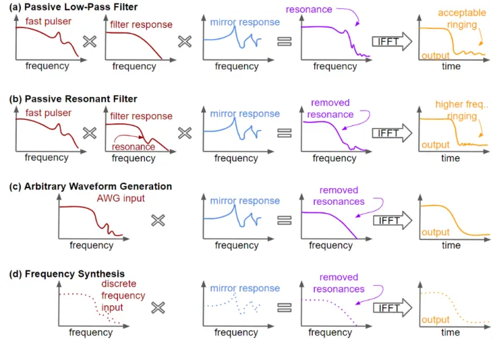
Ringing in the driving pulse using traditional high voltage techniques mentioned above can be ad-dressed with low-pass filtering, such as a Butterworth filter, which truncates higher-frequency compo-nents to the accuracy required while slowing the transition speed [59]. This is shown schematically in Fig. 2.2a. An alternative approach that does not reduce transition speeds as much is to use resonant filters on the output, which selectively block out the parasitic resonances, shown in Fig. 2.2b. However, this is difficult to implement, especially at the high voltages required, and further difficulties are introduced by the requirement of being able to adjust the pulse width from 30 ns to 150 ns, which changes the frequency content of the pulse.
Impedance mismatch between input lines and the mirror, which causes ringing in the load due to the mirror acting as a resonator, can be addressed in four ways. The first, easiest approach is to bring the pulser close to the load. However, due to the size of the pulsers, as well as their thermal dissipation, this is not possible for a gated mirror held under vacuum. A second simple approach is to simply shrink the mirror electrodes. This shifts the resonances developed over the length scale of the load up, meaning they will be less excited by a pulse of a given bandwidth. Another, more sophisticated approach would be to make the mirror roughly 50 Ω by engineering its geometry into a parallel plate structure. However this approach, which is commonly used in deflector designs, has many practical difficulties when applied to a gated mirror. Examples include the need to drive the mirror at more than 10 keV, which requires tapered electrodes near the the insulator connections, and complexities from having a hole in the structure.
The fourth, most complicated approach, is to use resonant matching, either with lumped elements or strip-lines, to selectively match each frequency component of the pulse to 50 Ω. If the repetition rate of the pulsing is fixed at say 5 MHz, this means that we need to manipulate frequency components at 5 MHz intervals to achieve a given pulse shape. However, given our need for sub-10 ns transitions to 1%we need more than 500 MHz of bandwidth, meaning we theoretically need to account for over 100 frequency
Figure 2.2: Approaches to precision high frequency driving. (a) Traditional low-pass filtering, where the entire edge is slowed to remove ringing in the driving and avoid load resonances. (b) Resonant filtering, where resonances and ringing components are selectively removed, allowing faster edges. (c) An AWG approach, where predistortion of the pulse allows for active removal of ringing and resonances. (d) Fre-quency synthesis approach, where we mix many discrete frequencies (shown as dots) to reconstruct a waveform at a given repetition rate.
points still. Granted, this is greatly simplified by fact that there are only a handful or resonances in a real load that we need to fit the magnitude, phase, and frequency of, but this problem is still very difficult due to the interaction of difference resonances. Again, the fact that we hope to adjust the pulse width and repetition rates for optimal performance complicates this as well and means separate filters for each pulse length would likely be required. One positive note on this technique is that it could probably be used in combination with the resonant ringing filtering approach, but this complicates the design still further.
Another approach would be to totally abandon the use of traditional fast, high voltage pulsers and instead use modern digitally controlled waveform generators and power amplifiers. These offer a possible solution to this filtering problem, since in this case we can simply program in the required frequency components without worrying about complicated interactions. This also allows us to dynamically adjust both repetition rates and pulse widths as required. This could be achieved either by the use of frequency mixing at the given repetition rate to achieve a desired arbitrary pulse (shown for discrete frequencies in Fig. 2.2d, or through the use of fast time-domain sampling from an arbitrary waveform generator shown in Fig. 2.2d. Due to the huge amount of frequency components required of a mixing approach (more than 100, calculated above) the AWG approach seems much more feasible. Commercial AWGs exist with bandwidths of 50 gigasamples per second, such as the Tektronix AWG70000B, although they generally output at most 5 volts. Power amplifiers rated to over 100 V with bandwidths up to 500 MHz also exist, such as the ZHL-100W-GAN+ from MiniCircuits, which address this problem. Many concerns still exist with this approach, such as the stability of AWG, drift in the system, and amplifier noise, and it is an active area of research in the QEM collaboration [39, 60]. An alternative approach to power amplifiers would be to have impedance transforming lines going from 50 Ω to 1 kΩ, which would increase the line voltage from 5 V to 100 V, at the expense of complicating the structure and introducing more system resonances. All of these approaches are compared in Fig. 2.2.
In this work, we take a completely different approach to switching of the gated mirror, taking advantage of emerging high-speed and high-power Gallium Nitride field effect transistors (GaNFETs) and using them directly as switches. While GaNFETs have been used extensively for high-efficiency power converters [61], amplifiers [62], and pulsed lasers [63], we demonstrate that these devices have the potential to also switch a gated electron mirror due to their sub-nanosecond rise times and > 200 V voltage ratings. These circuits are also simple to control due to their FET topology, with single-shot pulsing triggered by a 5 V logic inputs up to a repetition rate of 60 MHz which allows us to easily set both the pulse width and repetition rate of our mirror without any tuning. The high power efficiency and low thermal dissipation of these circuits also offer advantages in operation, leading to small form factors that are compatible with
vacuum environments. This vacuum compatibility means that these circuits can be integrated directly into gated electron mirrors, removing the need for impedance matching by removing the need for transmission lines and allowing us to simply damp the gated mirror as an resistor-inductor-capacitor (RLC) load with minimized parasitics due to its small size.
Chapter 3
Design of Gallium Nitride High Voltage
Pulsers
Wide bandgap semiconductors such as Gallium Nitride (GaN) have long been considered excellent candi-dates for power electronics due to their ability to withstand voltage and currents far beyond that of silicon, low channel resistances, and high temperature compatibility [64]. In recent years, GaN on silicon tech-nology has emerged as a low cost and robust option with commercial products that have small gate and output capacitances, optimized packages to minimize parasitic inductances, and a wide variety of current and voltage ratings [65]. Along with these advances, various fast single-sided and half-bridge drivers with sub-ns rise times, 7 A of peak drive current, 60 MHz repetition rates, and 2.5 ns propagation delays have been demonstrated [66]. Together, these offer the possibility of few-nanosecond switching of hundreds of volts and tens of amperes, ideal for application to a gated electron mirror.
In this section, we first validate the capabilities of these GaNFET circuits, demonstrating switching in under 1 ns of up to 200 V. We optimize the circuit design, layout, and filtering to minimize circuit parasitics and ensure vacuum compatibility. Using high voltage passive probing, we demonstrate 100 V transitions and ringing-free switching of this circuit, and test the maximum power of such circuits. Next, we connect the circuit to an oscilloscope through a decoupling capacitor to avoid introducing probing artifacts to our measurements and see the transition with as little perturbation as possible. We use this same approach to approximate real distributed loads as well. Finally, we share designs for a double sided GaNFET pulser, and details for the assembly of such circuits.
Figure 3.1: Circuit diagram for the GaNFET, where the gate driver is the LMG1020, and GaNFET the EPC2012C. Rgatedamps the gate turn on loop (G), Rdamp damps the fast load loop (L1), and Rbias sets
the power usage and load recovery time loop (L2). The optional trimming circuit in red allows for fine tuning of the load damping.
3.1
Single-Sided Circuit Design
In order to validate the possibility of GaN for switching a gated electron mirror, we first designed a testing circuit from the LMG1020 driver from Texas Instruments along with the EPC2012C enhancement mode GaNFET from the Efficient Power Corporation. The basic circuit design is shown in Fig. 3.1. The load is held to potential Vbias until the gate driver is triggered by Vtrig. When the driver is triggered, the gate
driver outputs a high current signal through Rgateto turn on the GaNFET by charging its gate as shown in
loop G. Charge is then shunted out from both the GaNFET’s parasitic output capacitance and the arbitrary load through Rdampinto ground (loop L1), bringing the load bias to zero. When the GaNFET is shut back
off, Vbiaspulls the voltage back up through Rbiasin loop L2, though this transition is significantly slower
due to the larger value of Rbias, which limit power dissipation circuit when the GaNFET is on. If we wanted
to speed this up, a high voltage P-channel silicon MOSFET could be used in place of the resistor, though this would require active control. The resistors Rgateand Rdampare also used to set the turn on time and
damp the ringing for the FET and the load, respectively. A tunable snubbing circuit, based on a trimming capacitor as shown in red, was incorporated to ensure that the transition was critically damped, since the RF damping resistors used had values too coarse to precisely damp the circuit.
The full circuit used is shown in Fig. 3.2a, with part numbers labeled. The power supply is based on the TPS7A4700RGWT (Texas Instruments), though any low-noise direct current (DC) supply will suffice. In order to minimize switching times and ringing, significant care was taken to choose capacitors with high self resonant frequencies (SRFs) and low equivalent series resistances (ESRs) for the driving circuitry. We placed the capacitors as close to the LMG1020 driver as possible, as shown in Fig. 3.2b. We used the
Label(s) Value Manufacturer Part Number C6 0.1µF Murata Electronics NFM15PC104D0J3D C7 1µF TDK Corporation C0510X5R0J105M030BC
C8 20 pF Vishay Vitramon VJ0603D200JXPAJ
C9 8 - 40 pF Knowles Voltronics JZ400HV
R1, R2 2 Ω Vishay Dale CRCW02012R00FXED
R3 1 kΩ Bourns Inc. CR0603-JW-102ELF
R4, R5 10 Ω Vishay Thin Film FC0402E10R0BTT0 R6, R7 25 Ω Vishay Thin Film FC0402E25R0BTT0 J2, J5 12 GHz Murata Electronics MM5829-2700RJ4 Table 3.1: List of components from schematic shown in Figure 3.1
combination of a 0.1 µF 0402 feed-through capacitor (TDK YFF15PC0J474MT) closest to the driver and a 1µF 0204 (wide package) capacitor (TDK C0510X5R0J105M030BC) slightly further out to provide a low-impedance drive loop and maintain biasing to the driver respectively. The temperature stability of the capacitors was sacrificed in order to minimize the package sizes used, with X5R ratings chosen rather than X7R. Low heat dissipation in our system and good thermal grounding ensured this did not cause problems in our setup due to changing capacitance with temperature. The most relevant parts and part numbers used are listed in table 3.1.
We also sought to minimize the size of the drive ground loop in order to minimize parasitic inductance in our circuit. This was done by the use of a thin two-sided 100 µm Kapton substrate (PCBWay) with a direct ground return trace running under from the GaNFET source pad directly to the driver ground as shown in Fig. 3.2b.
Damping was implemented using high-frequency thin film resistors ranging from 10 Ω to 100 Ω (Vishay Thin Film FC Series). Though the 0.125 W power rating would indicate they can only operate to 1.25 MHz (assuming 100 V switching of 10 pF), we found the resistor continued working to 5 MHz. Us-ing better heat-sinkUs-ing and multiple dampUs-ing resistors in parallel to spread out the dissipation, we found this circuit could operate up to 20 MHz, the maximum repetition rate we tested. This performance was limited by the resetting time of Rbias, and we began to see the voltage failing to return to zero if the repe-tition rate was too high. In the test cases shown, we used two parallel 10 Ω resistors for damping, which we calculated as roughly the critical damping point. This testing was done using a LeCroy PP007-WR 500 MHz probe, which slowed the response but ensured we could not damage the oscilloscope.
We were also able to make these circuits vacuum compatible. This was done by using silver-based solder (SMD291SNL-ND from Chip Quik Inc.) and low-out-gassing Kapton substrates (PCBWay). After assembly, the circuits were mounted on Oxygen-free high conductivity (OFHC) copper, sonicated in PCB
Figure 3.2: Test-bed circuit schematics and layout. (a) The main part of the circuit design, excluding the power supply which is represented by VCC. (b) The layout. The active region is to the right. Note the proximity of the input capacitors to the LMG1020 and the minimized ground return path placed directly under the drive loop to minimize inductance.
Figure 3.3: The physical layout of the circuit mounted on a flexible Kapton substrate. The highlighted green region shows the active portion of the circuit which is <0.25 cm2.
cleaning solution (PELCO Kleensonic™ APC) rinsed by water and IPA, and finally encased in thermally conductive and electrically insulating ceramic epoxy (EPO-TEK H70E Thermally Conductive Epoxy).
Figure 3.3 shows the realization of this circuit on a 100 µm thick Kapton substrate. The green shaded region shows the active area of the GaNFET, driver, bypass capacitors and damping, taking up less than 0.25 cm2, while the power supply makes up the rest of the circuit and can be placed off-board. No difference was seen between having the power supply directly on the board or coupled in via a coaxial cable. The circuit shown is not yet mounted to OFHC copper or encased in epoxy.
A detailed description of the assembly is described at the end of this chapter.
3.2
Circuit Testing
We then tested the response of the circuit with a 500 MHz, 10 MΩ probe (LeCroy PP007-WR) on a 2 GHz LeCroy 6200A oscilloscope. The exact contact, using a blade ground attachment, is shown in Fig.3.4a. The setup used is shown in Fig. 3.13 in the testing section at the end of this chapter.
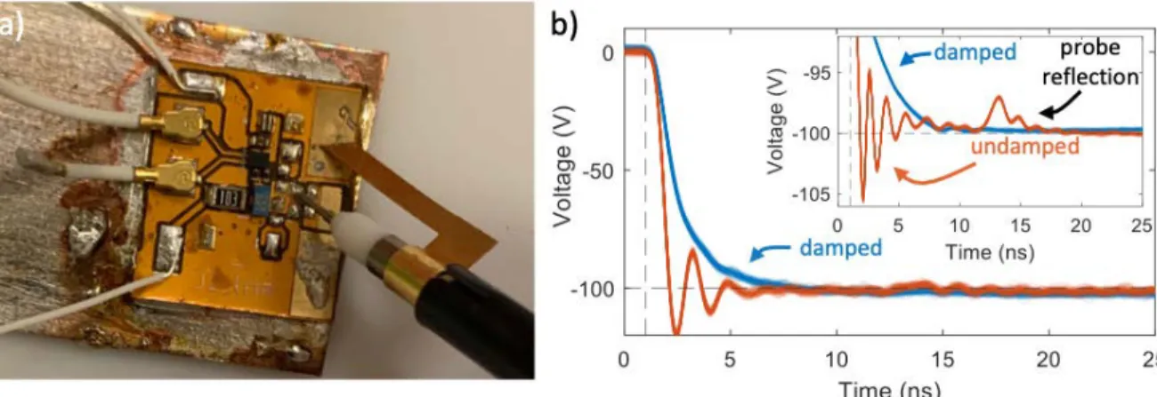
The undamped response at Rdamp = 0 Ω shows a full transition in less than 1 ns, but suffers from
significant ringing. This is shown in Fig. 3.4. Note that there is a second spurt of ringing around 12 ns. Given the cable is 1.2 m long, and the speed of light in the cable is 66% the speed of light in vacuum, we get that a return reflection would occur in 12 ns, leading us to believe this is the cause despite the engineering of the cable by the manufacturer to prevent return reflections. We believe the high power of the switching makes this small, 2% reflection (which is not of interest for standard applications of lower voltage or speed) visible.
Figure 3.4: Probing of the circuit. (a) Probing using a high impedance high voltage probe. (b) Output of probe. The undamped result shows significant ringing and a resurgent ringing we attribute to probing cable reflections. The damped result shows fully removed ringing in a 3 ns transition.
The near-critically damped response obtained at Rdamp = 25 Ω and by tuning the trimming circuit
(setting Rtrim = 15 Ω and Ctrim ≈ 40pF ) shows a transition from -10 V to -90 V (10% to 90% of the
amplitude) in less than 3 ns with no residual ringing. More significantly, the critically damped circuit is capable of reaching 5% of the final value in under 4 ns, and 1% accuracy in 6 ns as shown in the top right inset of Figure 3.4b. We note that these circuits were successfully driven up to 200 volts. However, to ensure we did not damage the probe and oscilloscope in the overshoot cases, the maximum voltage we used while measuring was 100 V.
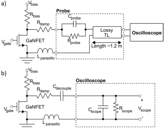
This measurement established the approximate speed and voltage capabilities of our circuit, but does not accurately represent what a lumped load would behave as. To remove probe artifacts, as well as most accurately simulate a real load of short length, we directly hooked the circuit up to the oscilloscope, as shown in Fig. 3.5a.
This direct connection was done instead of the more standard approach of using active probing, since most active probes are not rated for high enough voltages for our testing and the full system is hard to analyze. Also, as will be explained in Chapter 4, the large length scale of a probe and its cable interferes with our attempts to approximate the system as lumped elements, meaning that the damping of the system is not straightforward. A comparison of the two measurement approaches is shown in Fig. 3.6, with the most important difference being the lossy transmission line of Fig. 3.6a. Fig. 3.6b does not have this length scale and so can be reduced to lumped elements. The passive probe also has compensation circuitry consisting of low and high-pass adjustable filtering, which complicates the model, though ideally this is removable through compensation.
chang-Figure 3.5: Direct hookup of the circuit to the oscilloscope. The PCB is directly connected to the oscilloscope through an SMA connector decoupled by a 2.2 pF capacitor.
Figure 3.6: Measurement circuit models. (a) is the measurement circuit model using the 500 MHz probe, which has unavoidable transmission line effects due to its length of 1.2 m. For simplicity the compensation circuits are neglected. (b) the simpler model from directly hooking the circuit up to the oscilloscope. Due to the proximity of the circuit to the measuring amplifier, we can neglect transmission line effects. A decoupling capacitor is used to prevent impedance changes the GaNFET sees when switching gains, and to attenuate the input voltage.
Figure 3.7: Effect of changing gain on the measurement. (a) A trace with a gain of 1.02 V/division. (b) The same trace with a gain of 1.00 V/division. Switching this range causes an audible click in the oscilloscope, likely due to some sort of switched amplifier configuration on the input, which visibly changes the response of the circuit.
ing as a function of the oscilloscope gain. This is demonstrated below in Fig. 3.7a and b for 1 V/division and 1.02 mV/division respectively, and is repeated for other transitions such as from 100 mV/division to 102 mV/division where the waveform changes more subtly. We hypothesize that this is due to changes in the oscilloscope amplifier impedance as we switch gain ranges, which changes what the GaNFET sees. In-troducing a small-valued capacitor in series to stabilize the impedance seen by the circuit seems to improve this, though not entirely.
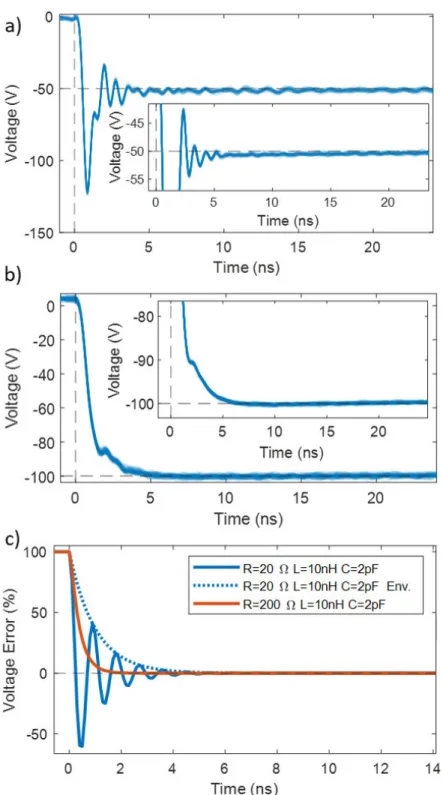
We then measured the decoupled circuit with and without damping. In Fig. 3.8a we used a 2.2 pF capacitor, resulting in a 1:10 attenuation into the 20 pF, 1 MΩ oscilloscope load. The resulting load is 2 pFas seen by the GaNFET. We only drove to 50 V to avoid damage to the oscilloscope, since the ringing overshoot is significant, reaching a peak of -125 V. We measure the ringing to be 1.1 GHz.
Because the GaNFET to oscilloscope distance is much smaller than the wavelength of the largest transi-tion frequency, we can simplify this circuit into a resistor-capacitor-inductor (RLC) circuit model. Knowing the ringing frequency (f) and that our total capacitance (C) is 3 pF ( 2 pF from the scope and 1 pF from the substrate), we use L ≈ 1
(2πf )2C to estimate an inductance of 7 nH. Given RG-58/U cable has an inductance
of 3.67 nH/cm, this would mean our circuit is 2 cm from the oscilloscope amplifier, which seems to be on the order of the dimensions of our circuit. If we have an RLC-type circuit, this would then mean we would
Figure 3.8: (a) A 2.2 pF decoupling capacitor with no damping biased to 50 V (b) The same decoupling, with 200 Ωresistive damping. (c) RLC-model comparison to the curves with and without damping.
expect to need total damping of R = 2 ∗qL
C, which is 96.6 Ω.
We the apply a 100 Ω resistor in series with the decoupling capacitor, making this circuit slightly over-damped. This results in a transition from 10% to 90% of the amplitude in less than 1.5 ns with no residual ringing. More significantly, the critically damped circuit is capable of reaching 1% of the final value in under 3 ns. This demonstrates that the GaNFETs are potentially fast and high-voltage enough to drive a gated electron mirror with very high accuracy.
3.3
Double-Sided Pulsing
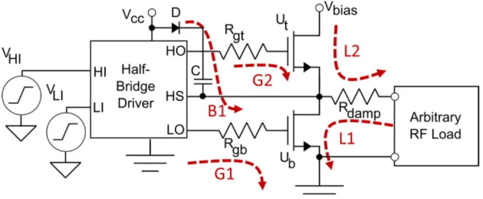
Finally, we extended this design to a double-sided pulser using bootstrapped GaNFETs based on the LMG1210 driver from Texas Instruments. The basic operation of this circuit is described in Fig. 3.9. We begin by describing the low side loop, which is similar in operation to the first circuit based on the LMG1020. We begin with both GaNFETs off, isolating the gated mirror node at HS. First, VLI is set high while VHIis set low. This turns off the top GaNFET Utand turns on the bottom one by shunting current though loop G1 into the gate of Ub. This allows the load to be pulled to ground through Rdamp, which damps the circuit. At the same time, loop B1 pulls current from Vccthrough diode D into capacitor C, charging it to 5 V (Vcc) above the level of pin HS.
Next, we shut off the bottom GaNFET Ub by setting VLI low, again isolating the gated mirror until needed. After a set delay, determined by the number of round trips in the cavity, we set VHI high, which begins putting current through loop G2 into the gate of Ut. As the FET opens, HS is pulled high to Vbias, and because the diode D shuts off, capacitor C is able to hold the high-side GaNFET Ut’s gate signal (HO) to be 5 V above Vbias. This keeps the GaNFET Utopen, allowing the load to be pulled high through Rdamp. Once this is completed, we set VHI to low, and the cycle repeats.
As before, we show the schematic and layout in Fig. 3.10a and b, and the parts used in this circuit in Tab. 3.2. The primary difference between the LMG1020 and LMG1210 based designs stem from the need for a bootstrapping reservoir to hold the upper GaNFET to the gate potential, and the need to have a low-impedance charge reservoir across Vbiasto sink into the gated mirror when generating the positive edge. This bootstrapping circuitry necessarily adds to the physical size of the layout, and internally in the driver, slowing performance. The required biasing capacitors must also be carefully chosen to minimize self-resonances that slow turn on times. The layout and part selections address both of these factors. Other details include the use of biasing capacitors on the input, selection of low-ESR capacitors for the internal regulator, and use of a Schottky diode and a feed-through capacitor to minimize reverse recovery time,
Figure 3.9: Operating description of the bootstrapped GaNFET circuit, allowing for both positive and neg-ative voltage transitions.
Label(s) Value Manufacturer Part Number
C1 10µF TDK Corporation C3216JB1C106K160AA C2, C3 1µF TDK Corporation C2012X7S2A105K125AE C4 1µF Murata Electronics NFM15PC104D0J3D C5 0.1µF TDK Corporation C0510X5R0J105M030BC C6 250 V 0.1 µF TDK Corporation CGA4J3X7T2E104M125AE C7 250 V 0.022 µF TDK Corporation C20123X7R2E223K125AA C8 250 V 330 pF Vishay Vitramon VJ085D331KXPAJ C9,10,11 250 V 100 pF Vishay Vitramon VJ063D101KXPAJ
C12 40 pF Knowles Voltronics JZ400HV
R1, R2 2 Ω Vishay Dale CRCW02012R00FXED
R3, R4, R5 10 Ω Vishay Thin Film FC0402E10R0BTT0
D1 10 Ω Vishay Thin Film FC0402E10R0BTT0
J1, J2 12 GHz Murata Electronics MM5829-2700RJ4 Table 3.2: List of components from schematic shown in Fig. 3.10
voltage drops, and loop inductance.
The response of this circuit is shown in Fig. 3.11, using a passive 500 MHz, 10 MΩ probe (LeCroy PP007-WR) on a 2 GHz LeCroy 6200A oscilloscope as before. The undamped transitions are 2 ns, slower than the single-sided case due to the larger loop inductance of the circuit and the slower driver.
In the following sections on simulating and testing the gated mirror, we will focus on the single-sided topology, since its faster switching leads to more stringent constraints on the design of the gated mirror and damping. All of this analysis applies equally well to the case of this bootstrapped pulser, which is the easier case given the lower frequency content of its switching.
Figure 3.10: Bootstrapped GaNFET circuit design. As before, we sought to minimize ground loop sizes by using small components, thin substrates, and careful placement.
Figure 3.11: Bootstrapped GaNFET Results. (a) The physical circuit, which is significantly larger than the initial topology, taking up less than 2 cm2. (b) Double-sided pulsing demonstration into a 500 MHz probe. The response is slower due to the larger circuit size. Vertical scale is 20 V/division, horizontal scale is 10 ns/division.
3.4
Assembly Procedure
The following details the construction of this high-speed GaN circuit.
1. First, we prepare our work space. Electrostatic discharge (ESD) safe mats and grounding bracelets are a necessity to get high circuit yields. Preheat the hot plate to 190°C. Preheat a soldering iron to 300°C. Tape the circuit using an easy release masking tape to whatever work surface you hope to assemble it on, as shown in Fig. 3.12a.
2. Next, we use a soldering stencil from the layout given (also from PCBway) and align it using a magnifying glass or microscope to the pattern. Tape one side of the mask as shown with the flipped stencil in Fig. 3.12a. We found aligning to the smallest component pads was the easiest way to do this.
3. Apply a small amount of solder paste to the edge of the mask. Holding the stencil firmly and evenly down, use a straight edge (such as a plastic card) to gently spread the paste over all of the holes, ensuring each hole is covered. Then, pressing more strongly on the card, scrape away any excess material.
4. Remove the stencil, being careful to pop it directly up. Inspect the layout, ensuring there are no solder connections between different pads. If there are, it is possible to correct by breaking the bridges with a fine tip. If the paste is too spread out, wipe the surface clean and repeat. An example of good looking paste application is shown in Fig. 3.12b.
Figure 3.12: Overview of circuit assembly for thermal management and vacuum compatibility. (a) Taping of the circuit to the board, and the stencil attached to the left with tape (flipped upside-down). (b) Solder paste clearly on pads, resulting from a well-aligned stencil. (c) Heating of the circuit on a hot plate to solder each connection. Also shown is the solder spread on the copper mount, which we place the circuit on for heat-sinking. (d) the final circuit without wires, showing successful soldering of the components and bonding to the copper heat sink.
5. Now assemble components. If not already done, make sure to wear an ESD bracelet, or at least ground your tweezers with an alligator clip or something similar. Even the slightest discharge will destroy the GaNFET, causing your FET to be across the source to drain when off. This is especially catastrophic in the double-sided circuit as it can damage your high voltage supply. Other various tips are below.
• Begin assembling components one at a time. Generally we start with the largest components and work down in size, finishing with the EPC2012c and LMG1020 as their pads are the most delicate and they are the most expensive. The only exception to this size rule is placing R1 and R2, which we generally do fairly early since they are inexpensive and easy to mess up, and it is nice to have space to place them without worrying about knocking the GaNFETs or driver out of place.
• Various methods exist for stabilizing hands while doing this such as resting your hand on your fingers, exhaling during the final component placement, and avoiding caffeinated beverages the day of trying. Using a clean wipe and alcohol, clean the tweezers after each placement to prevent solder paste from sticking the component to the tweezers.
• If the component is misplaced, put the tweezers tip onto the PCB to stabilize shaking, and then slide the tweezers tip around to nudge components into place. As long as the component pads make contact with the solder paste on each pad, it should be fine as surface tension will pull components exactly into place.
6. Place the circuit onto the hot plate. If available, place a fume extractor or fan above the hot plate. Increase the plate temperature to 290°C, though this can be adjusted depending on the plate, as long as the PCB does not darken the temperature is not too high. As this happens, you should see the solder begin to melt. Watch the smallest components, especially the LMG1020 and EPC2012c, and make sure the components get pulled into place by surface tension of the solder. If this does not happen, try slightly nudging the components with tweezers to knock them into place. If when you touch the components, there is no action trying to return them to place, they are likely not properly placed, or there is not enough solder.
7. On the piece of OFHC copper you wish to mount your circuit on, spread out the silver solder paste evenly. For our thin heat sink this is shown in Fig. 3.12c. Remove the assembled circuit and place it onto the copper. The solder should harden holding the circuit components in place. Now, place the
entire copper piece onto the hotplate. Wait until the solder melts and the circuit is pulled into place by surface tension.
8. Reduce the hot plate temperature to 190°C. Wait until all of solder re-solidifies. Once this happens, take the soldering iron and apply it to the biasing and power pads and solder on connection wires. Remove the circuit. Clean the circuit with acetone and IPA. If vacuum performance is required, sonicate in PCB cleaning solution given in the materials section. If high repetition rate performance is required, encase in EPO-TEK H70E thermally conductive epoxy (PELCO). The end product should look like Fig. 3.12d.
3.5
Circuit Testing Procedure and Safety
1. Next, we test the circuit. First connect the circuit to ground. Next, attach the high voltage biasing port to a high voltage port. In our case, we used a 150 V piezo supply (Thorlabs model MDT693B) with a 1 MΩ resistor tied to ground (for safety and ESD protection) coupled through a BNC cable (rated to 300 V). This high voltage supply is left off until testing. We then turn on the power supply supply. In early tests we used a 6 V power supply (XP Power VEL05US060-US-JA) with the designed regulator circuit. For later tests, to reduce power dissipation in the circuit and it more vacuum compatible, we used a 5 V direct connection from a low noise power supply (Keithley Model 2220). We saw no difference in results using either source.
2. We then hook up the RF ports. We used an SMA-to-JSC adapter (GradConn CABLE 366 RF-200-A) and BNC-to-SMA adapter to get the input signal from the signal generator (Keysight 33250A) to the driving board. For traces shown, we input a 3 v, 100 ns wide pulse with 5 ns rising edges at a repetition rate of 1 kHz. This low rate was chosen to reduce the voltage offset in AC-coupling and reduce thermal effects, though the circuit was tested to 20 MHz, limited by the recharge time of the biasing resistor and breakdown of the biasing. The second input was grounded.
3. We then turned on the high voltage supply, starting at 5 V to ensure the circuit functioned properly. Once this was verified we slowly increased to voltage to the set point. For initial tests we used a LeCroy PP007-WR 500 MHz 10 MΩ probe, tested up to 100 V with a blade ground connector, as shown in Fig. 3.13. The probe was compensated using a 1 MHz square wave signal from the oscilloscope.
Figure 3.13: Testing setup used, showing shielding, ground insulation, and probing.
4. For the final testing, we directly hooked up our circuit through an SMA connector which we adapted to a BNC connector and inserted into the oscilloscope. This is shown in Fig. 3.5a.
Chapter 4
Simulation of Pulser Switching
Performance in Real Loads
In this section, we simulate the performance of several gated electron mirror structures. We then interact these mirrors with a simulation of our GaNFET circuit to validate the GaNFET’s switching performance, demonstrating ringing-free critical damping of the mirror. We compare this to results from a low-pass filtering approach. In these simulations, we focus on the single-sided pulser, which is faster and with higher frequency content, although all of this work applies equally well to double-sided pulsers as well. We discuss the theoretical limits to switching speeds for a gated mirror, which is fundamentally set by the length scale of the structures. Finally, we simulate other loads to demonstrate the generality of this GaNFET switching approach.
4.1
Integrated Simulations of a Gated Mirror
In order to validate the performance of the GaNFET pulser for quantum electron microscopy, we simulated its performance when interacting with a gated electron mirror. We chose to do this using frequency-domain simulations. We chose to simulate the mirror in the frequency frequency-domain because the gated mirror is a linear time-invariant (LTI) load, and so solving the mirror in the frequency domain gives all information about its performance. Then, by creating a circuit model fit to this, we were able to fully interact it with a non-linear time domain simulation in LTSpice. This approach of combining time and frequency domain simulations dramatically improved simulation speed and performance, as well as gave greater physical intuition to the problem.