HAL Id: hal-02550925
https://hal-cnrs.archives-ouvertes.fr/hal-02550925
Submitted on 11 Dec 2020
HAL is a multi-disciplinary open access
archive for the deposit and dissemination of
sci-entific research documents, whether they are
pub-lished or not. The documents may come from
teaching and research institutions in France or
abroad, or from public or private research centers.
L’archive ouverte pluridisciplinaire HAL, est
destinée au dépôt et à la diffusion de documents
scientifiques de niveau recherche, publiés ou non,
émanant des établissements d’enseignement et de
recherche français ou étrangers, des laboratoires
publics ou privés.
Yb-doped zinc tin oxide thin film and its application to
Cu(InGa)Se2 solar cells
Youngsang Park, Gerald Ferblantier, Abdelilah Slaoui, Aziz Dinia,
Hyeonwook Park, Salh Alhammadi, Woo Kyoung Kim
To cite this version:
Youngsang Park, Gerald Ferblantier, Abdelilah Slaoui, Aziz Dinia, Hyeonwook Park, et al..
Yb-doped zinc tin oxide thin film and its application to Cu(InGa)Se2 solar cells. Journal of Alloys and
Compounds, Elsevier, 2020, 815, pp.152360. �10.1016/j.jallcom.2019.152360�. �hal-02550925�
UNCORRECTED
PROOF
Journal of Alloys and Compounds xxx (xxxx) xxx-xxx
Contents lists available at ScienceDirect
Journal of Alloys and Compounds
journal homepage: www.elsevier.comYb-doped zinc tin oxide thin film and its application to Cu(InGa)Se
2
solar cells
Youngsang Park
a, Gérald Ferblantier
b, Abdelilah Slaoui
b, Aziz Dinia
c, Hyeonwook Park
a, Salh Alhammadi
a,
Woo Kyoung Kim
a,∗aSchool of Chemical Engineering, Yeungnam University, Gyeongsan, Gyeongbuk, 38541, Republic of Korea bICube, CNRS-Université de Strasbourg, UMR 7357, 23 rue du Loess, BP 20 CR, 67037, Strasbourg Cedex 2, France cIPCMS, CNRS-Université de Strasbourg UMR 7504, 23 rue du Loess, BP 43, 67034, Strasbourg Cedex 2, France
A R T I C L E I N F O
Article history:
Received 1 May 2019
Received in revised form 17 September 2019 Accepted 19 September 2019
Available online xxx
Keywords:
Ytterbium Zinc tin oxide Cu(InGa)Se2
Solar cell Down-converter
A B S T R A C T
The use of rare earth elements with semiconductor materials has attracted immense interest due to their unique properties. In this study, we investigated the characteristics of an ytterbium (Yb)-doped zinc tin oxide (Yb:ZTO) thin film and its application as a potential down-converter of Cu(InGa)Se2(CIGS) thin-film
so-lar cells. Yb:ZTO thin films were deposited by reactive sputtering of Zn and Sn metal with oxygen flow. A few pieces of Yb were embedded in a Zn metal target; thus Yb elements were supplied during Zn sputtering. The relative composition of Zn and Sn was controlled by changing the sputtering power (10–70W) of Sn, in relation to the fixed sputtering power for Zn (70 W). In addition, the substrate temperature was varied from room temperature to 400 °C. It was confirmed that a smaller amount of Sn with lower sputtering power led to more incorporation of Yb into ZTO. X-ray photoelectron spectroscopy analysis confirmed the incorporation of Yb into ZTO, and photoluminescence measurement demonstrated Yb emission. Grazing incidence X-ray diffraction indicated the shift of ZTO emission peaks induced by the difference in the composition of Zn and Sn. Finally, CIGS solar cells with an Yb:ZTO layer were fabricated. The results suggested that cells with the highest Yb photoluminescence emission showed the highest short-circuit current density and cell efficiency.
© 2019.
1. Introduction
Chalcopyrite Cu(InGa)Se2 (CIGS)-based thin film photovoltaic
cells have continuously broken the record of cell conversion efficiency over the last few decades, which is currently at 23.35% (Solar Fron-tier 2019) [1]– superior to polycrystalline Si (22.3% [2]) and thin film CdTe (21.0% [2]). The typical stack structure of CIGS cells follows the pattern substrate/Mo/CIGS/CdS/i-ZnO/ZnO:Al/grid, and various novel approaches on the individual stacked layers and interfaces have been explored to achieve a further increase in the cell performance [3–7]. Photon conversion effects including up-conversion, down-con-version, and down-shifting using modified transparent conductive lay-ers have been studied as promising approaches to enhance the cur-rent collection of photovoltaic cells [8–10]. The photon up-conversion converts two or more low energy (e.g., typically lower than the band gap energy of light absorber) photons to a single high energy photon with energy higher than the band gap energy of absorber. Down-con-version is the process to convert a high energy photon to multiple lower energy photons of which energy is still higher than the band gap energy. Both up- and down-conversion processes reduce the loss of light absorption and thus enhance the short circuit current density of solar cells [11].
∗Corresponding author.
Email address: wkim@ynu.ac.kr (W.K. Kim)
Several rare earth elements have been explored as potential can-didates for a photon converter, including Nd [12,13], Tm [13], Eu [14], Pr [15], Er [16], Yb [16,17], and Dy [18] for a ZnO matrix. Rare earth element-doped SnO2has been studied as well [9,10,19,20].
However, the study on the Zn–Sn–O (ZTO) matrix was hardly re-ported. ZTO material is inexpensive and chemically stable. Further-more, it can be deposited by abundant and non-toxic sources and thus considered a promising candidate as a substitute for indium-doped tin oxide and intrinsic ZnO transparent conductors. In addition, it pos-sesses both the optical transparency of ZnO and the excellent elec-trical conductivity of SnO2[21]. It is known that the structural and
optical properties of ZTO can be controlled by adjusting the com-position of Zn and Sn in ZTO [22]. Recently, Dimitrievska et al. tried to dope Eu3+ions into nanocrystalline Zn
2SnO4powders using a
mechano-chemical solid-state reaction method [23]. In this paper, the ytterbium (Yb)-doped ZTO (Yb:ZTO) thin film was investigated. In particular, the effects of the relative composition of Zn/Sn and sub-strate temperature during the co-sputtering process on Yb:ZTO were measured and optimized processing parameters determined. In addi-tion, the optimized Yb:ZTO layer was applied to Cu(InGa)Se2(CIGS)
thin-film solar cells. To the best of our knowledge, this is the first work to incorporate Yb into ZTO host, and investigate their compo-sitional effects on optical properties, and apply the Yb:ZTO to solar cells.
https://doi.org/10.1016/j.jallcom.2019.152360 0925-8388/ © 2019.
UNCORRECTED
PROOF
2 Journal of Alloys and Compounds xxx (xxxx) xxx-xxx
2. Materials and methods
Yb:ZTO thin films with a thickness of approximately 100 nm were prepared on 500μm-thick p-type Si wafers with (100) orientation and a 1 mm-thick glass substrate by the radio-frequency (RF) reac-tive-magnetron sputtering method with flowing Ar and O2at 8 sccm
and 3 sccm, respectively. The Yb-doped Zn (Yb:Zn) and pure Sn tar-gets were simultaneously sputtered at the sputtering power of 70 W (fixed) and 10–70W(varied), respectively. The Zn (or Yb:Zn) and Sn targets have a 2 inch-diameter disk shape. The Yb:Zn alloy target was prepared by implanting several pieces of small Yb pure metal (99.99%, 70 g each) onto a pure Zn target. The substrate temperature varied from 100 to 400 °C during initial experiments (to be optimized afterward.) The information on Sn sputtering power (10–70W) and substrate temperature (100–400°C) can be found in the sample ID. For example, sample S10T3 represents 10 W power and 300 °C substrate temperature. During the sputtering process, the working pressure was maintained at 3.4 mTorr (∼0.4533Pa) and the substrate was located approximately 12 cm above the target. For lateral homogeneity of film thickness, the substrate was rotated. The deposition rate was varied from approximately 3 nm/min (for S10T3) to 20 nm/min (for S70T3) depending on the sputtering power of Sn target, which was estimated by measuring the thickness of film after each deposition. Two halogen lamps were located behind the sample holder for heating the substrate. The Yb:ZTO thin film has been employed as a transparent con-ducting oxide to replace an i-ZnO layer in a conventional CIGS so-lar cell structure of glass/Mo/CIGS/CdS/i-ZnO/Al:ZnO/grid, as shown in Fig. 1. A p-type CIGS light absorbing layer with a thickness of 1.5–1.7μm was fabricated by the reaction of CuGa/In bilayer metal precursors with H2Se and H2S gas. Bilayer CuGa/In precursors were
deposited on Mo-coated glass by the sequential DC sputtering of a CuGa alloy (∼24 wt% Ga) and pure In targets, yielding a total CuGa/In thickness of 500 − 600 nm and atomic composition of Cu/( Ga + In) = 0.85 − 0.95 and Ga/(Ga + In) = 0.2 − 0.3. The selenization of CuGa/In precursors by H2Se gas was performed at 480–500°C
for 25–35min, and then followed by the sulfurization by H2S gas at
550–580°C for 60–90min.
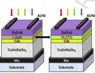
The n-type buffer layer of CdS (∼70nm) was deposited by chem-ical bath deposition. Yb:ZTO with a thickness of 100 nm was then deposited on CdS as a photon converter layer, followed by the DC sputter-deposition of n-type Al:ZnO (AZO) with a thickness of about
Fig. 1. Schematic diagram of CIGS solar cell structure: (left) conventional structure and (right) new structure with Yb:ZTO fabricated in this study.
400 nm. Finally, a Ni/Ag front grid was deposited by electron beam evaporation at room temperature.
The crystallography of the as-deposited Yb:ZTO thin films was analyzed by grazing incidence X-ray diffraction (GI-XRD; PANa-lytical X'Pert PRO MPD) with CuKα1radiation (λ=0.154056nm) at
an incidence angle ofω=0.4°. The thickness of the thin films was measured using a spectroscopic ellipsometer (HORIBA Uvisel™ Lt M200 FGMS) in the range of 210–880nm. The doping concentration of Yb in the ZTO thin films was estimated by X-ray photoelectron spectroscopy (XPS, K-Alpha) surface scans at operating conditions of 400μm spot size, 200eV pass energy, 0.1eV step size, and the con-stant analyzer energy (CAE) mode. A photoluminescence (PL) mea-surement was carried out in the 300–1050nm range of wavelength using a frequency-tripled neodymium-doped yttrium aluminum gar-net (Nd-YAG) laser with a wavelength of 355 nm. PL signals enter into an optical fiber and then are analyzed by a multi-channel CCD. The transmittance of the thin film was measured by a spectropho-tometer (U-Perkin-Elmer Lambda 950) in the wavelength range of 300–1300nm. The current-voltage (I–V) characteristics of the CIGS solar cells were identified using a solar simulator (K3000 XE55 Solar Cell I–V Measurement System) with AM1.5 irradiation.
3. Results and discussion
3.1. Effect of ZTO composition
Fig. 2 presents the GI-XRD (ω=0.4°) patterns of Yb:ZTO thin films deposited at different Sn sputtering powers of 10–70W, with a fixed Yb:Zn alloy sputtering power of 70 W and substrate temperature of 300 °C. The XRD patterns of all samples except S10T3 look quite broad due to the probable formation of ZnO–SnO2or Zn–Sn–O
al-loys, which have been reported to be amorphous below approximately 450 °C [22,24]. However, S10T3 samples prepared using the lowest sputtering power (10 W) of the Sn target show sharp hexagonal ZnO (002) and (103) peaks by XRD analysis [25,26], as summarized in Table 1; they also have only 1.31 at.% Sn with Sn/(Zn + Sn)∼ 0.02. Apparently, the increased Sn sputtering power resulted in the de-creased intensity of the ZTO peak and its slight shift to a lower 2θ position, demonstrating the formation of more amorphous and higher Sn-containing ZTO. The low crystallinity of ZTO is partly attribut-able to the formation of stress by the different sizes of Zn and Sn ions [22]. In addition, increased Sn concentration may lead to the formation of SnO (JCPDS: 06-0395), SnO2(JCPDS: 41-1445), and other
oxy-gen-rich ZTO compounds such as spinel Zn2SnO4(JCPDS: 24-1470)
and ilmenite ZnSnO3(JCPDS: 52-1381) [24]. However, the Yb
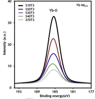
dop-ing concentration decreased with increased Sn sputterdop-ing power. The chemical composition of ZTO alloys has been estimated by XPS analysis. Fig. 3 presents peaks near 185 eV corresponding to the Yb 4d5/2core level of atoms bound to oxygen, confirming the
formation of Yb-Zn-Sn-O structure rather than the elemental Yb of which bind energy is near 182-183 eV [27]. Even though the Yb ion can exist in a 2 + oxidation state, it is hardly detected by XPS due to the very small difference in binding energy [28]. As shown in Fig. 3 and Table 1, the doping concentration of Yb in ZTO mo-notonically decreases with the sputtering power of the Sn target. In general, during doping, the crystalline structure of the host mater-ial is preferred to the amorphous structure because there are more available doping sites in crystalline materials than amorphous ones. For example, the wurtzite ZnO structure has empty tetrahedral and octahedral sites, which can be occupied by dopants, i.e., interstitial
UNCORRECTED
PROOF
Fig. 2. GI-XRD patterns of the Yb:ZTO thin films deposited by different Sn sputteringpowers in the range of 10–70W. Table 1
Composition estimated by XPS spectra of Yb:ZTO films deposited at different Sn sput-tering power. Sample Zn 2p (at.%) Sn 3d (at.%) Sn/(Zn + Sn) O 1s (at.%) Yb 4d (at.%) Band gap (eV) S10T3 52.2 1.31 0.02 46.2 0.25 3.28 S20T3 40.8 12.8 0.24 46.2 0.18 3.33 S30T3 31.2 17.0 0.35 51.6 0.17 3.80 S40T3 21.6 21.0 0.49 57.2 0.12 3.70 S70T3 4.57 22.2 0.83 73.1 0.09 3.10
doping [29]. In addition, the grain boundary of a polycrystalline struc-ture can be used as a penetration path for dopants [28]. However, the reduced crystallinity of the ZTO matrix by adding Sn, and thus increasing structural disorder, may restrict the incorporation of Yb. The oxygen content approximately increases with increased Sn in-corporation due to a higher oxidation state of Sn than Zn, i.e., SnO2
vs. ZnO. Considering the stoichiometry of each film, S10T3 is close to ZnO; with increasing sputtering Sn power the film composition changes successively to Zn3SnO4, Zn2SnO3, ZnSnO3, and SnO2from
the S20T3 to the S70T3 samples, respectively. From XPS results, it was confirmed that Yb was incorporated from the crystalline structure to amorphous structure.
The optical activation of the Yb:ZTO thin films was investigated using PL spectroscopy. The PL spectra of Yb:ZTO thin films pre-pared by different Sn sputtering power were obtained using a 355 nm
Fig. 3. Yb 4d5/2XPS spectra of Yb:ZTO films as a function of Yb:Sn sputtering power.
Nd:YAG laser. These are shown in Fig. 4. The strong and sharp peaks detected at 355 nm and 710 nm correspond to the laser source. A very weak intensity observed from the S10T3 sample near 380 nm in the UV region may result from band-to-band transitions. The broad peaks in the range of 500–850nm of the visible light region identified from most of the samples are believed to be produced mainly by defect states. Even though their origin is still controversial, they are presum-ably associated with intrinsic defects such as oxygen vacancies and in-terstitial atoms [28]. For the S20T3 sample, a sharp and strong peak was detected near 975 nm; it is presumably associated with the radia-tive transition of the 2F
5/2excited state to the 2F7/2 ground state of
the Yb3+ion. A satellite broad peak located at about 1010 nm is con-sidered energy level splitting induced by the Stark effect in the Yb level. A similar observation was reported by Balestrieri et al. who studied a ZnO thin film Yb-doped by reactive sputtering [17]. The Yb characteristic peak near 975 nm was also found in the S30T3 sample
UNCORRECTED
PROOF
4 Journal of Alloys and Compounds xxx (xxxx) xxx-xxx
with a relatively weak intensity, but not detected in the other samples (S30T3 to S70T3) prepared with higher Sn sputtering power.
A more detailed comparison of peaks in the visible light region re-vealed that the peak intensity of the S10T3 and S20T3 samples was highest and similar to each other, and the intensity of the others de-creased with inde-creased Sn incorporation. This peak attenuation can be explained by several contributions. Firstly, the increase of Sn concen-tration reduces the crystallinity of ZTO, as shown in Fig. 2, and atomic disorder in an amorphous compound can produce the defect states causing non-radiative recombination [30,31]. Similarly, Karmakar et al. reported that the disorder introduced in a Mn-doped ZnO thin film led to the decrease of crystallinity and PL intensity [30]. In our study, as the Sn concentration increases, the more amorphous condition of the ZTO thin film can generate a dangling bond state yielding the competitive pathways for transitions between energy levels, and thus restricting PL emission in the visible light region, as schematically represented in Fig. 5. Secondly, the higher Sn incorporation into the ZTO structure increases oxygen concentration in ZTO as well, and reduces oxygen vacancies, which are usually responsible for the PL process. Lastly, it is assumed that the expansion in the energy band gap of the ZTO film with increased Sn concentration can limit the band-to-band excitation causing the reduction of PL intensity. For ex-ample, the estimated energy band gap of the S30T3 and S40T3 sam-ples (S30T3: 3.80 eV, S40T3: 3.70 eV) is larger than that of the laser (3.49 eV≅355nm) and thus the excitation from valence band to con-duction band can be decreased. The drastic decrease of peak intensity in the S30T3 sample (with the highest band gap∼3.8eV) may be due to this reason.
As shown in Fig. 6, the S40T3 and S70T3 samples have a de-creased band gap and inde-creased oxygen vacancy, but showed lower PL intensity compared with S30T3, which suggests that the increased density of the dangling bond defect from an amorphous structure restricts the energy transfer. In general, the O1s peak can be de-convoluted into three peaks; a peak with the highest binding en-ergy (∼532.3eV) corresponds to oxygen in hydroxide, and one with middle energy (∼531.7eV) is for oxygen in an oxygen deficient re-gion. The peak with the lowest energy (∼530.3eV) belongs to
Fig. 5. Schematic energy band diagram of absorption and emission transitions in Yb:ZTO.
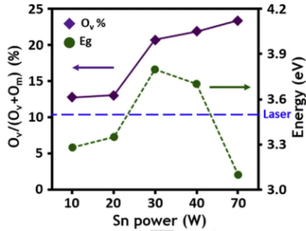
Fig. 6. Ratio of oxygen vacancy concentration estimated by O1s XPS spectra, and band gap energy (Eg) calculated by transmittance for Yb:ZTO films as a function of Sn sput-tering power.
oxygen surrounded by Zn and Sn atoms. In this study, it was con-firmed that O1s XPS spectra of all Yb:ZTO films were deconvoluted into only two characteristic peaks. The Ompeak near low binding
en-ergy is commonly related to oxygen binding with metal such as Zn, Sn atom, and the OVpeak near high binding energy is to oxygen in an
oxygen deficient region [32]. The OV/(Om+ OV) ratio with Sn
sputter-ing power is shown in Fig. 6. However, the lowest peak intensity was similarly observed from S70T3 samples having a lower energy band gap (S70T3: 3.10 eV) than the laser, which suggests that the effect of the band gap on the attenuation of the PL peak may not be dominant.
The Yb peak at 975 nm had the highest intensity in sample S20T3, and the intensity drastically decreased with increased Sn amount (S30T3 to S70T3). However, the sample with the smallest Sn amount (S10T3) showed much lower intensity compared with S20T3 presum-ably due to a concentration quenching effect. When the amount of op-tically active rare-earth ions increases to a certain level, the excitation energy is not transferred through a radiative transfer mechanism any longer; instead, it is transferred non-radiatively between dopant ions resulting in a reduced luminescence efficiency. Similar concentration quenching effects were also reported by other research groups in stud-ies on Tb-doped SnO2[33] and Nd-doped SnO2[34] thin films. The
attenuation of the Yb characteristic PL peak with increased Sn concen-tration can be attributed to the following reasons. Firstly, as similarly observed in the visible light region, more Sn incorporation into ZTO tends to increase the amorphous nature of the host compound and, thus, the density of dangling bond states to capture carriers, thereby restricting energy transfer from host to Yb ions. Secondly, the reduced density of internal defect states with increased Sn concentration can limit the PL efficiency of Yb, as illustrated in Fig. 5. It has been re-ported that the intrinsic or extrinsic defect states of the host material can enhance the energy transfer from the host to the rare earth ions [35]. Salarie et al. tried to enhance light emission using cooperative transitions with defect states produced by oxygen vacancies in the host material [36]. Thirdly, the reduced Yb amount with increased Sn con-centration as analyzed by XPS (Table 1) might be another reason for the reduced Yb PL intensity. However, considering the small differ-ence of Yb concentration, the effect of variation in the energy states of host materials, such as defect states and dangling bond states, will be more dominant than that of Yb concentration.
The PL results in Fig. 4 suggest that the down-conversion effect has been confirmed by the PL emission in both visible light and the near-infrared (NIR) region with the 355 nm incident UV laser. In ad
UNCORRECTED
PROOF
dition, it should be noted that the scale of the y-axis for the Yb peak (at 975 nm) is 10 times larger than that for the peak in the visible light region, thus illustrating that the NIR PL emission of the Yb peak is much stronger than that in visible light. This suggests that ZTO can be a good host material for efficient energy transfer, and Yb light with a wavelength of 975 nm (∼1.27eV) may be applicable for a CIGS-based (Eg∼1.2eV) thin film solar cell.
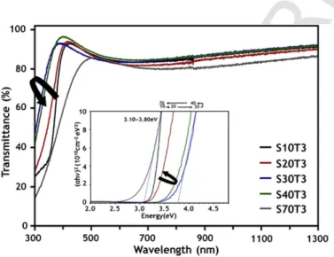
The optical transmittance of Yb:ZTO thin films prepared onto glass substrates was investigated in the range of 300–1300nm wave-length. As shown in Fig. 7, most films, notably except S70T3, exhib-ited considerable transmittance of over 80% in the visible region. With the increase of Sn sputter power from 10 W to 30 W, the left absorp-tion edge of the curve, i.e., the shortest wavelength region, shifted to-ward the left while it moved to the opposite direction with further in-crease of Sn sputter power from 30 W to 70 W. The left shift of the absorption edge with increased Sn sputter power (10–30W) may be attributed to the increased energy band gap by the Burstein-Moss ef-fect [37]; that is, the energy band gap of ZTO increases by adding Sn as an electron donor because Sn has four valence electrons compared to Zn having two valence electrons. In contrast, the right shift of the absorption edge in the higher Sn sputter power (30–70W) can be ex-plained by structural properties. As shown in Fig. 2, the enhanced in-corporation of Sn into ZTO films by increasing Sn sputter power can make ZTO films more amorphous; thus, this leads to the formation of a localized band tail state, due to the structural disorder, yielding a re-duced band gap and lower transmittance [22].
As shown in the inset of Fig. 7, the energy band gap of ZTO films was estimated by using the Tauc plots [38] based on the absorption edge of the transmittance curve, assuming the direct transition be-tween valence and conduction bands. The estimated values of the en-ergy band gap were in the range of 3.10–3.80eV, which is similar to those reported by other research groups [37,39]. Young et al. reported that crystalline ZTO thin films deposited by the sputtering technique showed a direct optical band gap in the range 3.3–3.9eV, which was influenced by Burstein-Moss shift effect and structural dissimilarity of the ZTO thin films [37]. As mentioned in the previous paragraph, the band gap became wider with increased Sn sputter power from 10 to 30 W (Eg = 3.28–3.80eV), and then reduced with further increase from 30 to 70 W (Eg = 3.80 to 3.10 eV).
Fig. 7. UV–vis–NIR optical transmittance of Yb:ZTO thin films for different Sn sput-tering power, and corresponding energy band gaps estimated by Tauc plot (inset).
3.2. Effect of substrate temperature
It has been reported that the deposition temperature has a strong influence on photoluminescence of rare-earth atoms in host materials such as ZnO and SnO2[10,17]. To investigate the effect of substrate
temperature during the sputtering process of Yb:ZTO, the substrate temperature was varied from 100 to 400 °C while the sputtering power of Zn and Sn were held constant at 70 W and 20 W, respectively. Con-sidering the subsequent fabrication of working solar cells, the maxi-mum temperature was limited to 400 °C.
The structural and compositional properties of Yb:ZTO films were investigated by GI-XRD and XPS analyses. The results of the GI–XRD, shown in Fig. 8, revealed that there is no significant dif-ference in shape and intensity of the characteristic ZTO peak at 2θ=32–34°, which is not strong and thus nearly amorphous. It has also been reported that ZTO films maintain an amorphous nature up to 500–600°C [40,41]. Choi et al. suggested that the stability of the amorphous ZTO phase below 600 °C is attributed to the immis-cible system of pseudo-binary ZnO and SnO2[41]. As temperature
increased from 100 to 400 °C, the characteristic peak of ZTO near 2θ=32–34° shifted slightly to a lower 2θ position, presumably due to atomic rearrangement. It can be assumed that the increased temper-ature can supply thermal energy for further rearrangement of atoms within the amorphous structure. Furthermore, higher temperature can cause atomic vacancies to be occupied, thus yielding the lattice ex-pansion and the left shift of XRD peak. The composition estimated by XPS spectra of the Yb:ZTO films prepared at different substrate temperature, i.e., the deposition temperature, is summarized in Table 2. The overall composition of Sn/(Zn + Sn) for thin films deposited at a substrate temperature in the range of 100–400 °C was 0.239–0.253, indicating nearly a stoichiometric Zn3SnO4ternary phase.
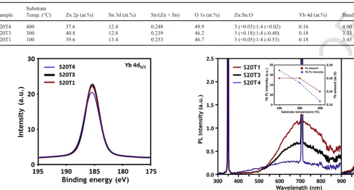
As shown in Fig. 9 and summarized in Table 2, the incorpora-tion of Yb into ZTO decreased at the highest substrate temperature of
Fig. 8. GI–XRD patterns of the Yb:ZTO thin films deposited at different substrate tem-peratures: 100 °C (T1), 300 °C (T3), and 400 °C (T4).
UNCORRECTED
PROOF
6 Journal of Alloys and Compounds xxx (xxxx) xxx-xxx
Table 2
Composition estimated by XPS spectra of Yb:ZTO films deposited at different substrate temperatures. Sample
Substrate
Temp. (°C) Zn 2p (at.%) Sn 3d (at.%) Sn/(Zn + Sn) O 1s (at.%) Zn:Sn:O Yb 4d (at.%) Band gap (eV)
S20T4 400 37.6 12.4 0.248 49.9 3 (+0.03):1:4 (+0.02) 0.16 4.00
S20T3 300 40.8 12.8 0.239 46.2 3 (+0.18):1:4 (-0.40) 0.18 3.33
S20T1 100 39.6 13.4 0.253 46.7 3 (+0.05):1:4 (-0.53) 0.18 3.45
Fig. 9. Yb 4d5/2XPS spectra of Yb:ZTO films deposited at different substrate
tempera-tures: 100 °C (T1), 300 °C (T3), and 400 °C (T4).
Fig. 10. Ratio of oxygen vacancy concentration (diamonds) estimated by O1s XPS spec-tra and band gap (circles) calculated by spec-transmittance for Yb:ZTO films deposited at different substrate temperatures: 100 °C (T1), 300 °C (T3) and 400 °C (T4).
400 °C, compared to 100 °C and 300 °C. This can be explained by the decrease of available doping sites in the ZTO host because the atomic rearrangement of active Zn and Sn atoms is enhanced at high temper-ature, the doping sites are preoccupied. Therefore, it can be assumed that a too-high temperature may not be beneficial to the incorporation of Yb into the ZTO compound under a crystallization phase, due to its immiscible nature (see Fig. 10).
As displayed in Fig. 11, PL measurements have been carried out to investigate the effect of deposition temperature on the photolumi-nescence properties of Yb:ZTO films. Apparently, an increase in tem-perature from 100 to 400 °C did not generate new peaks in the mea-sured wavelength range of 300–1050nm. As temperature increased from 100 to 400 °C, the defect band near the visible light region de-creased. The intensity of the Yb PL peak at 975 nm was also re-duced. This decrease in visible emission can be explained by sev
Fig. 11. PL spectra of Yb:ZTO films deposited at different substrate temperatures.
eral contributions. As indicated in the previous XPS result, oxygen va-cancies, which induce visible PL emission, were decreased at 300 °C, and thus the PL intensity decreased as well. In addition, the area of grain boundaries increased, due to the formation of ZnO grains. The grain boundaries usually cause non-radiative recombination; thus ra-diative emission was relatively decreased [42]. The significant de-crease at 400 °C may be attributed to the high band gap of the film (∼4.0eV), which is larger than the laser excitation energy, thus reduc-ing the excitation from the valence band. This increase in band gap will be discussed further in the next section. The decrease in the inten-sity of Yb PL emission is proportional to the amount of electrons in ra-diative defect transition. At 300 °C, while the number of excited elec-trons might be larger than that at 100 °C, due to a decreased band gap, it seems that energy transfer to the Yb atoms decreased because of a non-radiative defect center. At 400 °C, the number of excited electrons decreased further, resulting in the decreased transfer to the Yb atoms. Furthermore, the decreased number of Yb atoms at 400 °C could con-tribute to the decreased PL emission of Yb. The PL results indicate that despite the same number of Yb ions in the film, the properties of the ZTO host strongly influence its PL emission. From the PL mea-surement, a high PL emission is favorable in the ZTO host at a rela-tively low temperature within the amorphous state.
To investigate the effect of deposition temperature on transmit-tance of Yb:ZTO films, the transmittransmit-tance was measured in the 300–1300nm range, as displayed in Fig. 12. The values of the corre-sponding energy band gap were extracted by using a Tauc plot as in the figure inset. The transmittance of films with the deposition tem-perature of 100–400°C showed over 80% in the entire wavelength region. It was revealed that the energy band gap of Yb:ZTO film slightly decreased (3.45–3.33eV) or remained the same as the depo-sition temperature was raised from 100 to 300 °C, but it noticeably increased up to 4.0 eV as temperature reached 400 °C. This dramatic increase might be attributed to the increased oxygen vacancies with
UNCORRECTED
PROOF
Fig. 12. UV–vis–NIR optical transmittance of Yb:ZTO thin films for differentdeposi-tion temperatures, and corresponding energy band gaps estimated by Tauc plot (inset).
increased temperature. It was reported that oxygen vacancies in a TCO thin film act as donor-producing excess carriers, changing the energy band gap by means of the Burstein-Moss (BM) effect [43]. In addition, the increase in band gap of Yb:ZTO at a deposition temperature of 400 °C resulted in the shift of the transmittance plot to the low wave-length region, as coincidently shown in Fig. 12. It is well known that high deposition temperatures in semiconductor thin films can produce oxygen deficient films [43,44]. This is because oxygen desorption oc-curs in metal oxide materials at high temperatures due to the low for-mation energy of oxygen vacancies. At 300 °C, however, the tion of oxygen vacancies was restricted, presumably due to the forma-tion of ZnO.
3.3. Application to solar cells
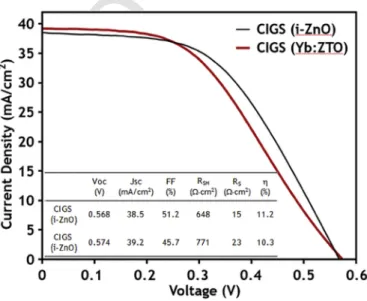
Based on the above study of ZTO properties by changing Sn sput-ter power and substrate temperature during co-sputsput-tering of Sn and Zn in a flowing oxygen environment, we determined the potentially opti-mized conditions of 15 W Sn sputter power and 100 °C substrate tem-perature. These conditions were employed to deposit another set of Yb:ZTO films. As shown in Fig. 13, the Yb PL peak intensity of the Yb:ZTO film deposited at these sputtering conditions is greater than those of the other films in the study, suggesting better energy trans-fer efficiency. Therefore, these sputtering conditions were employed to deposit an Yb:ZTO film for the fabrication of a glass/Mo/CIGS/ CdS/Yb:ZTO:AZO solar cell. The current–voltage characteristics of this cell are compared with those of a conventional glass/Mo/CIGS/ CdS/i-ZnO/AZO solar cell in Fig. 14. It is interesting to note that the overall cell efficiency of CIGS cell with Yb:ZTO (η=10.3%) is nearly equivalent to that of a conventional CIGS cell with i-ZnO (η=11.2%). It seems that the slight increase in Jsc and Voc of the Yb:ZTO-CIGS cell was offset by the loss of fill factor (i.e., 51.2%–45.7%). Slight increase of VOC(i.e., 0.568–0.574V) might be resulted from the
in-crease of shunt resistance (RSH) (i.e., 648 to 771Ωcm2). The improved
Jsc (38.5–39.2mA/cm2) can be explained by down-conversion effect
of Yb:ZTO layer leading to more absorption and collection of photons demonstrated by EQE results later.
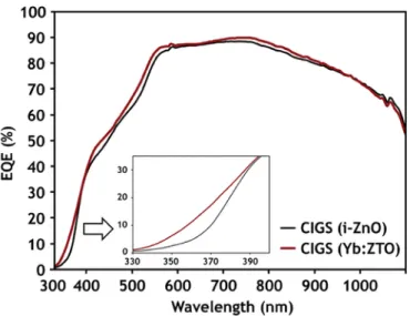
The external quantum efficiency plot of Fig. 15 confirmed that the Yb:ZTO-CIGS cell demonstrated enhanced quantum efficiency, com
Fig. 13. PL spectra of Yb:ZTO films deposited at different sputter conditions: Sn sput-ter power of 10, 15, 20 W and substrate temperature of 100 and 300 °C.
Fig. 14. Current–voltage characteristics of Yb:ZTO-incorporated CIGS solar cell and reference (i-ZnO) cell.
pared to the conventional i-ZnO-CIGS cell. This is particularly so in the UV region (inset of Fig. 15), presumably because of the photon conversion effect. To make sure that the increase of quantum effi-ciency was due to the down-conversion effect but not the increased light absorption, the absorption by the Yb:ZTO and i-ZnO layers was compared by means of reflectance and transmittance measurements. It was observed that the reflectance and transmittance of the Yb:ZTO films were greater than those of i-ZnO film (see Supporting Data), thus supporting the claim that the enhanced quantum efficiency was not caused primarily by increased light absorption. It was also con-firmed that the conductivity of a film was not improved by adopting Yb:ZTO, as noticed by the crossover of the EQE plot at the wave-length of 900–1000nm. Therefore, the detailed study on the other rea-sons for enhanced EQE suggested that the Yb:ZTO layer acts as a pho-ton converter. Further optimization of Yb doping, such as Yb concen-tration, deposition temperature, and film thickness may improve the optoelectronic properties of the Yb:ZTO film and the corresponding CIGS device performance.
UNCORRECTED
PROOF
8 Journal of Alloys and Compounds xxx (xxxx) xxx-xxx
Fig. 15. External quantum efficiency plot for Yb:ZTO incorporated CIGS solar cell and reference (i-ZnO) CIGS cell.
4. Conclusion
Yb:ZTO films were prepared by reactive co-sputtering of Yb:Zn and Sn targets, and their crystallographic and optoelectronic proper-ties were thoroughly investigated by changing Sn sputtering power (10–70W) to determine ZTO composition, and substrate temperature (100–400°C). It was demonstrated that Yb PL emission is signifi-cantly affected by the defect state in the ZTO host; it can be controlled by the amount of Sn in the ZTO and the substrate temperature during deposition. The results of the PL analysis suggested that the efficiency of energy transfer from host to Yb ions was highest for a sample pre-pared at a substrate temperature of 100 °C, in the range of 100–400°C. As this study shows, the highest performance Yb:ZTO-CIGS solar cell has been fabricated by adopting Yb:ZTO deposited at the suggested optimum conditions of 15 W Sn sputter power and 100 °C substrate temperature. The potential photon converting effect of Yb:ZnO film was supported by the observation of increased quantum efficiency without an increase of light absorption.
Acknowledgment
This study was supported by Priority Research Centers Program through the National Research Foundation of Korea (NRF) funded by the Ministry of Education (2014R1A6A1031189) and“Human Re-sources Program in Energy Technology” of the Korea Institute of En-ergy Technology Evaluation and Planning (KETEP), granted financial resource from the Ministry of Trade, Industry & Energy, Republic of Korea. (No. 20174030201760).
Appendix A. Supplementary data
Supplementary data to this article can be found online at https:// doi.org/10.1016/j.jallcom.2019.152360.
References
[1] A. Colthorpe, Solar Frontier Achieves CIS Thin-Film Lab Efficiency Record of 23.35%, 2019 https://www.pv-tech.org/news/solar-frontier-achieves-cis-thin-film-efficiency-record-of-23.35, Accessed 1 February 2019, accessed.
[2] M.A. Green, Y. Hishikawa, E.D. Dunlop, D.H. Levi, J.H. Ebinger, M. Yoshita, A.W.Y. Ho-Baillie, Solar cell efficiency tables (Version 53), Prog. Photovolt. Res. Appl. 27 (2019) 3–12 https://doi.org/10.1002/pip.3102.
[3] D. Lee, K. Yong, Non-vacuum deposition of CIGS absorber films for low-cost thin film solar cells, Korean J. Chem. Eng. 30 (2013) 1347–1358 https://doi.org/ 10.1007/s11814-013-0101-0.
[4] V.B. Chu, S.J. Park, G.S. Park, H.S. Jeon, Y.J. Hwang, B.K. Min, Semi-trans-parent thin film solar cells by a solution process, Korean J. Chem. Eng. 33 (2016) 880–884 https://doi.org/10.1007/s11814-015-0200-1.
[5] S.K. Lee, H.J. Jeong, Y.C. Kim, J.H. Jang, Improvement in CIGS solar cell effi-ciency using a micro-prism array integrated with sub-wavelength structures, Sol. Energy Mater. Sol. Cells 186 (2018) 254–258 https://doi.org/10.1016/j.solmat. 2018.06.045.
[6] R.L. Garris, S. Johnston, J.V. Li, H.L. Guthrey, K. Ramanathan, L.M. Mansfield, Electrical characterization and comparison of CIGS solar cells made with differ-ent structures and fabrication techniques, Sol. Energy Mater. Sol. Cells 174 (2018) 77–83 https://doi.org/10.1016/j.solmat.2017.08.027.
[7] P.M.P. Salomé, J. Keller, T. Törndahl, J.P. Teixeira, N. Nicoara, R.-R. Andrade, D.G. Stroppa, J.C. González, M. Edoff, J.P. Leitão, S. Sadewasser, CdS and Zn1− xSnxOy buffer layers for CIGS solar cells, Sol. Energy Mater. Sol. Cells 159 (2017) 272–281 https://doi.org/10.1016/j.solmat.2016.09.023.
[8] D. Chen, Y. Wang, M. Hong, Lanthanide nanomaterials with photon manage-ment characteristics for photovoltaic application, Nano Energy 1 (2012) 73–90 https://doi.org/10.1016/j.nanoen.2011.10.004.
[9] K. Bouras, J.-L. Rehspringer, G. Schmerber, H. Rinnert, S. Colis, G. Ferblantier, M. Balestrieri, D. Ihiawakrim, A. Dinia, A. Slaoui, Optical and structural proper-ties of Nd doped SnO2powder fabricated by the sol–gel method, J. Mater. Chem.
C. 2 (2014) 8235–8243 http://doi.org/10.1039/C4TC01202J.
[10] K. Bouras, G. Schmerber, H. Rinnert, D. Aureau, H. Park, G. Ferblantier, S. Co-lis, T. Fix, C. Park, W.K. Kim, A. Dinia, A. Slaoui, Structural, optical and elec-trical properties of Nd-doped SnO2thin films fabricated by reactive magnetron
sputtering for solar cell devices, Sol. Energy Mater. Sol. Cells 145 (2016) 134–141 https://doi.org/10.1016/j.solmat.2015.07.038.
[11] D. Verma, T.O. Saetre, O.-M. Midtgård, Review on up/down conversion materi-als for solar cell application, Proc. 38th IEEE Photovolt. Spec. Conf. (2012) 2608–2613, https://doi.org/10.1109/PVSC.2012.6318129.
[12] H. Park, S. Alhammadi, K. Bouras, G. Schmerber, G. Ferblantier, A. Dinia, A. Slaoui, C.-W. Jeon, C. Park, W.K. Kim, Nd-Doped SnO2and ZnO for
applica-tion in Cu(InGa)Se2solar cells, Sci. Adv. Mater. 9 (2017) 2114–2120 https://doi.
org/10.1166/sam.2017.3207.
[13] Y. Liu, W. Luo, R. Li, H. Zhu, X. Chen, Near-infrared luminescence of Nd3+and
Tm3+ions doped ZnO nanocrystals, Opt. Express 17 (2019) 9748–9753 https:// doi.org/10.1364/OE.17.009748.
[14] Y.-P. Du, Y.-W. Zhang, L.-D. Sun, C.-H. Yan, Efficient energy transfer in monodisperse Eu-doped ZnO nanocrystals synthesized from metal acetylaceto-nates in high-boiling solvents, J. Phys. Chem. C 112 (2008) 12234–12241 https: //doi.org/10.1021/jp802958x.
[15] H. Li, K. Luo, M. Xia, P.W. Wang, Synthesis and optical properties of Pr3 +-doped ZnO quantum dots, J. Non-Cryst. Solids 383 (2014) 176–180 https:// doi.org/10.1016/j.jnoncrysol.2013.04.028.
[16] Y. Bai, Y. Wang, K. Yang, X. Zhang, Y. Song, C.H. Wang, Enhanced upcon-verted photoluminescence in Er3+ and Yb3+codoped ZnO nanocrystals with and
without Li+ions, Opt. Commun. 281 (2018) 5448–5452 https://doi.org/10.1016/
j.optcom.2008.07.041.
[17] M. Balestrieri, G. Ferblantier, S. Colis, G. Schmerber, C. Ulhaq-Bouillet, D. Muller, A. Slaoui, A. Dinia, Structural and optical properties of Yb-doped ZnO films deposited by magnetron reactive sputtering for photon conversion, Sol. En-ergy Mater. Sol. Cells 117 (2013) 363–371 https://doi.org/10.1016/j.solmat. 2013.06.032.
[18] F. Gu, S.F. Wang, M.K. Lü, G.J. Zhou, D. Xu, D.R. Yuan, Structure evaluation and highly enhanced luminescence of Dy3+-doped ZnO nanocrystals by Li+
dop-ing via combustion method, Langmuir 20 (2004) 3528–3531 https://doi.org/10. 1021/la049874f.
[19] H. Bastami, E. Taheri-Nassaj, Synthesis of nanosized (Co, Nb, Sm)-doped SnO2
powders using co-precipitation method, J. Alloy. Comp. 495 (2010) 121–125 https://doi.org/10.1016/j.jallcom.2010.01.099.
[20] P. Psuja, W. Strek, Influence of concentration and sintering temperature on lumi-nescence properties of Eu3+:SnO
2nanocrystallites, J. Rare Earths 30 (2012)
627–631 https://doi.org/10.1016/S1002-0721(12)60102-1.
[21] T. Minami, H. Sonohara, S. Takata, H. Sato, Highly transparent and conductive zinc-stannate thin films prepared by RF magnetron sputtering, Jpn. J. Appl. Phys. 33 (1994) 1693–1696 http://doi.org/10.1143/JJAP.33.L1693.
[22] J.H. Ko, I.J. Kim, D. Kim, K.S. Lee, T.S. Lee, B. Cheong, W.M. Kim, Transpar-ent and conducting Zn-Sn-O thin films prepared by combinatorial approach, Appl. Surf. Sci. 253 (2007) 7398–7403 https://doi.org/10.1016/j.apsusc.2007.03. 036.
UNCORRECTED
PROOF
[23] M. Dimitrievska, T.B. Ivetic, A.P. Litvinchuk, A. Fairbrother, B.B. Miljevic,G.R. Strbac, A.P. Rodriguez, S.R. Lukic-Petrovic, Eu3+Doped wide band gap
Zn2SnO4semiconductor nanoparticles: structure and luminescence, J. Phys.
Chem. C 120 (2016) 18887–18894 https://doi.org/10.1021/acs.jpcc.6b05335. [24] T. Moriga, Y. Hayashi, K. Kondo, Y. Nishimura, K.-I. Murai, I. Nakabayashi,
Transparent conducting amorphous Zn-Sn-O films deposited by simultaneous dc sputtering, J. Vac. Sci. Technol. A 22 (2004) 1705–1710 https://doi.org/10.1116/ 1.1765658.
[25] G.A. Olatunji, A.T. Kola-Mustapha, O.D. Saliu, A.B. Alabi, O.I. Abiodun, N.O. Obisesan, Tramadol hydrochloride delivery by regenerated cellulose
nanofiber-TiO2-ZnO composites, Korean J. Chem. Eng. 35 (2018) 784–791
https://doi.org/10.1007/s11814-017-0314-8.
[26] S. Sehar, I. Naz, I. Perveen, S. Ahmed, Superior dye degradation using SnO2-ZnO hybrid heterostructure catalysts, Korean J. Chem. Eng. 36 (2019)
56–62 https://doi.org/10.1007/s11814-018-0159-9.
[27] D. Briggs, Handbook of X-Ray Photoelectron Spectroscopy, Heyden, London, 1977.
[28] E. Flage-Larsen, S. Diplas, Ø. Prytz, E.S. Toberer, A.F. May, Valence band study of thermoelectric Zintl-phase SrZn2Sb2and YbZn2Sb2: X-ray
photoelec-tron spectroscopy and density functional theory, Phys. Rev. B. 81 (1–7) (2010) 205204 https://doi.org/10.1103/PhysRevB.81.205204.
[29] Y.-B. Hahn, Zinc oxide nanostructures and their applications, Korean J. Chem. Eng. 28 (2011) 1797–1813 https://doi.org/10.1007/s11814-011-0213-3. [30] P. Karmakar, S.K. Neogi, A. Barnrjee, S. Bandyopadhyay, Structural;
morpho-logical; optical and magnetic properties of Mn doped ferromagnetic ZnO thin film, Appl. Surf. Sci. 263 (2012) 671–677 https://doi.org/10.1016/j.apsusc.2012. 09.133.
[31] K. Pita, Q.V. Vu, in: Y. Masuda (Ed.), Energy Transfer from Silicon Nanocrys-tals to Er3+Ions Embedded in Silicon Oxide Matrix, Nanocrysals, InTech,
Croa-tia, 2011, pp. 437–458, https://doi.org/10.5772/17490.
[32] Y. Zhao, G. Dong, L. Duan, J. Qiao, D. Zhang, L. Wang, Y. Qiu, Impacts of Sn precursors on solution-processed amorphous zinc-tin oxide films and their tran-sistors, RSC Adv. 2 (2012) 5307–5313 http://doi.org/10.1039/C2RA00764A. [33] F. Hild, L. Eichenberger, A. Bouché, X. Devaux, M. Stoffel, H. Rinnert, M.
Vergnat, Structural and photoluminescence properties of evaporated SnO2thin
films doped with rare earths, Energy. Procedia 84 (2015) 141–148 https://doi. org/10.1016/j.egypro.2015.12.307.
[34] H. Rinnert, P. Miska, M. Vergnat, G. Schmerber, S. Colis, A. Dinia, D. Muller, G. Ferblantier, A. Slaoui, Photoluminescence of Nd-doped SnO2thin films,
Appl. Phys. Lett. 100 (2012) 101908–101910 https://doi.org/10.1063/1.3692747.
[35] A. Layek, S. Banerjee, B. Manna, A. Chowdhury, Synthesis of rare-earth doped ZnO nanorods and their defect-dopant correlated enhanced visible-orange lumi-nescence, RSC Adv. 6 (2016) 35892–35900 http://doi.org/10.1039/
C6RA02278B.
[36] S. Salari, F.E. Ghodsi, A significant enhancement in the photoluminescence emission of the Mg doped ZrO2thin film by tailoring the effect of oxygen
va-cancy, J. Lumin. 182 (2017) 289–299 https://doi.org/10.1016/j.jlumin.2016.10. 035.
[37] D.L. Young, H. Moutino, Y. Yan, T.J. Coutts, Growth and characterization of radio frequency magnetron sputter-deposited zinc stannate, Zn2SnO4thin films,
J. Appl. Phys. 92 (2002) 310–319 https://doi.org/10.1063/1.1483104. [38] J. Tauc, R. Grigorovici, A. Vancu, Phys. Status solidi, optical properties and
electronic structure of amorphous germanium, Phys. Status Solidi 15 (1966) 627–637 https://doi.org/10.1002/pssb.19660150224.
[39] S.-W. Chang, K. Ishikawa, M. Sugiyama, Growth of amorphous Zn-Sn-O thin films by RF sputtering for buffer layers of CuInSe2and SnS solar cells, Thin
Solid Films 589 (2015) 408–411 https://doi.org/10.1016/j.tsf.2015.06.003. [40] I.-J. Lee, N.-E. Sung, K.H. Chae, R. Conley, Characterization of zinc–tin–oxide
films deposited by radio frequency magnetron sputtering at various substrate temperatures, Thin Solid Films 548 (2013) 385–388 https://doi.org/10.1016/j.tsf. 2013.08.067.
[41] Y.-Y. Choi, S.J. Kang, H.-K. Kim, Rapid thermal annealing effect on the charac-teristics of ZnSnO3films prepared by RF magnetron sputtering, Curr. Appl.
Phys. 12 (2012) S104–S107 https://doi.org/10.1016/j.cap.2012.05.014. [42] T. Matsumoto, H. Kato, K. Miyamoto, M. Sano, E.A. Zhukov, T. Yao,
Correla-tion between grain size and optical properties in zinc oxide thin films, Appl. Phys. Lett. 81 (2002) 1231–1233 https://doi.org/10.1063/1.1499991. [43] O. Tuna, Y. Selamet, G. Ayhun, L. Ozyuzer, High quality ITO thin films grown
by dc and RF sputtering without oxygen, J. Phys. D Appl. Phys. 43 (1–7) (2010), 055402 https://doi.org/10.1088/0022-3727/43/5/055402.
[44] F. Hai-Bo, Y. Shao-Yan, Z. Pan-Feng, W. Hong-Yuan, L. Xiang-Lin, J. Chun-Mei, Z. Qin-Sheng, C. Yong-Hai, W. Zhan-Guo, Investigation of oxygen vacancy and interstitial oxygen defects in ZnO films by photoluminescence and X-ray photoelectron spectroscopy, Chin. Phys. Lett. 43 (2010) 2108–2111 https: //doi.org/10.1088/0256-307x/24/7/089.