The MIT Faculty has made this article openly available.
Please share
how this access benefits you. Your story matters.
Citation
Li, Nanxi et al. "Broadband 2-µm emission on silicon chips:
monolithically integrated Holmium lasers." Optics Express 26, 3
(January 2018): 2220-2230 © 2018 Optical Society of America
As Published
http://dx.doi.org/10.1364/oe.26.002220
Publisher
Optical Society of America (OSA)
Version
Final published version
Citable link
https://hdl.handle.net/1721.1/129795
Terms of Use
Article is made available in accordance with the publisher's
policy and may be subject to US copyright law. Please refer to the
publisher's site for terms of use.
Broadband 2-µm emission on silicon chips:
monolithically integrated Holmium lasers
N
ANXIL
I,
1,2,*E
MIRS
ALIHM
AGDEN,
1Z
HANS
U,
1,3N
EETESHS
INGH,
1A
LFONSOR
UOCCO,
1M
INGX
IN,
1M
ATTHEWB
YRD,
1P
ATRICKT.
C
ALLAHAN,
1J
ONATHAND. B. B
RADLEY,
1,4C
HRISTOPHERB
AIOCCO,
5D
IEDRIKV
ERMEULEN,
1,3ANDM
ICHAELR. W
ATTS11Research Laboratory of Electronics, Massachusetts Institute of Technology, Cambridge, MA 02139, USA
2John A. Paulson School of Engineering and Applied Science, Harvard University, Cambridge, MA 02138, USA
3Current address: Analog Photonics, One Marina Park Drive, Boston, MA 02210, USA
4Current address: Department of Engineering Physics, McMaster University, 1280 Main Street West, Hamilton, Ontario L8S 4L7, Canada
5College of Nanoscale Science and Engineering, University at Albany, Albany, New York 12203, USA
Abstract: Laser sources in the mid-infrared are of great interest due to their wide applications
in detection, sensing, communication and medicine. Silicon photonics is a promising technology which enables these laser devices to be fabricated in a standard CMOS foundry, with the advantages of reliability, compactness, low cost and large-scale production. In this paper, we demonstrate a holmium-doped distributed feedback laser monolithically integrated on a silicon photonics platform. The Al2O3:Ho3+ glass is used as gain medium, which
provides broadband emission around 2 µm. By varying the distributed feedback grating period and Al2O3:Ho3+ gain layer thickness, we show single mode laser emission at
wavelengths ranging from 2.02 to 2.10 µm. Using a 1950 nm pump, we measure a maximum output power of 15 mW, a slope efficiency of 2.3% and a side-mode suppression ratio in excess of 50 dB. The introduction of a scalable monolithic light source emitting at > 2 µm is a significant step for silicon photonic microsystems operating in this highly promising wavelength region.
© 2018 Optical Society of America under the terms of the OSA Open Access Publishing Agreement
OCIS codes: (130.0130) Integrated optics; (130.3120) Integrated optics devices; (140.3460) Lasers; (130.2790)
Guided waves.
References and links
1. S. L. K. Scholle, P. Koopmann, and P. Fuhrberg, “2 um Laser Sources and Their Possible Applications,” in
Frontiers in Guided Wave Optics and Optoelectronics, B. Pal, Ed., ed: (InTech, 2010), pp. 471–500.
2. J. H. Taylor and H. W. Yates, “Atmospheric transmission in the infrared,” J. Opt. Soc. Am. 47(3), 223–226 (1957).
3. J. Luo, B. Sun, J. Liu, Z. Yan, N. Li, E. L. Tan, Q. Wang, and X. Yu, “Mid-IR supercontinuum pumped by femtosecond pulses from thulium doped all-fiber amplifier,” Opt. Express 24(13), 13939–13945 (2016). 4. K. van Dalfsen, S. Aravazhi, C. Grivas, S. M. García-Blanco, and M. Pollnau, “Thulium channel waveguide
laser in a monoclinic double tungstate with 70% slope efficiency,” Opt. Lett. 37(5), 887–889 (2012). 5. K. van Dalfsen, S. Aravazhi, C. Grivas, S. M. García-Blanco, and M. Pollnau, “Thulium channel waveguide
laser with 1.6 W of output power and 80% slope efficiency,” Opt. Lett. 39(15), 4380–4383 (2014).
6. J. Wu, Z. Yao, J. Zong, A. Chavez-Pirson, N. Peyghambarian, and J. Yu, “Single frequency fiber laser at 2.05 μm based on Ho-doped germanate glass fiber,” in Proc. SPIE 7195, Fiber Lasers VI: Technology, Systems, and
Applications (2009), paper 71951K.
7. A. Hemming, S. Bennetts, N. Simakov, A. Davidson, J. Haub, and A. Carter, “High power operation of cladding pumped holmium-doped silica fibre lasers,” Opt. Express 21(4), 4560–4566 (2013).
8. S. D. Jackson, F. Bugge, and G. Erbert, “High-power and highly efficient diode-cladding-pumped Ho3+-doped silica fiber lasers,” Opt. Lett. 32(22), 3349–3351 (2007).
#313867 https://doi.org/10.1364/OE.26.002220
9. C. V. Poulton, M. J. Byrd, M. Raval, Z. Su, N. Li, E. Timurdogan, D. Coolbaugh, D. Vermeulen, and M. R. Watts, “Large-scale silicon nitride nanophotonic phased arrays at infrared and visible wavelengths,” Opt. Lett.
42(1), 21–24 (2017).
10. S. Manipatruni, K. Preston, L. Chen, and M. Lipson, “Ultra-low voltage, ultra-small mode volume silicon microring modulator,” Opt. Express 18(17), 18235–18242 (2010).
11. Z. Su, N. Li, E. Salih Magden, M. Byrd, Purnawirman, T. N. Adam, G. Leake, D. Coolbaugh, J. D. B. Bradley, and M. R. Watts, “Ultra-compact and low-threshold thulium microcavity lasermonolithically integrated on silicon,” Opt. Lett. 41, 5708–5711 (2016).
12. T. Komljenovic, S. Srinivasan, E. Norberg, M. Davenport, G. Fish, and J. E. Bowers, “Widely tunable narrow-linewidth monolithically integrated external-cavity semiconductor lasers,” IEEE J. Sel. Top. Quantum Electron.
21(6), 214–222 (2015).
13. T. Komljenovic and J. E. Bowers, “Monolithically integrated high-Q rings for narrow linewidth widely tunable lasers,” IEEE J. Quantum Electron. 51, 1–10 (2015).
14. Purnawirman, N. Li, E. S. Magden, G. Singh, M. Moresco, T. N. Adam, G. Leake, D. Coolbaugh, J. D. B. Bradley, and M. R. Watts, “Wavelength division multiplexed light source monolithically integrated on a silicon photonics platform,” Opt. Lett. 42(9), 1772–1775 (2017).
15. A. D. Bristow, N. Rotenberg, and H. M. Driel, “Two-photon absorption and Kerr coefficients of silicon for 850– 2200nm,” Appl. Phys. Lett. 90(19), 191104 (2007).
16. N. Singh, M. Xin, D. Vermeulen, K. Shtyrkova, E. S. Magden, P. T. Callahan, N. Li, A. Ruocco, N. Fahrenkopf, and D. Coolbaugh, “Octave spanning supercontinuum generation in silicon from 1.1 μm to beyond 2.4 μm,” in
CLEO: Science and Innovations, 2017, paper STu4J. 7.
17. A. W. Fang, E. Lively, Y.-H. Kuo, D. Liang, and J. E. Bowers, “A distributed feedback silicon evanescent laser,” Opt. Express 16(7), 4413–4419 (2008).
18. R. Wang, S. Sprengel, G. Boehm, R. Baets, M.-C. Amann, and G. Roelkens, “Broad wavelength coverage 2.3 μm III-V-on-silicon DFB laser array,” Optica 4(8), 972–975 (2017).
19. H. Rong, R. Jones, A. Liu, O. Cohen, D. Hak, A. Fang, and M. Paniccia, “A continuous-wave Raman silicon laser,” Nature 433(7027), 725–728 (2005).
20. J. Liu, X. Sun, R. Camacho-Aguilera, L. C. Kimerling, and J. Michel, “Ge-on-Si laser operating at room temperature,” Opt. Lett. 35(5), 679–681 (2010).
21. S. Wirths, R. Geiger, N. von den Driesch, G. Mussler, T. Stoica, S. Mantl, Z. Ikonic, M. Luysberg, S. Chiussi, J. M. Hartmann, H. Sigg, J. Faist, D. Buca, and D. Grützmacher, “Lasing in direct-bandgap GeSn alloy grown on Si,” Nat. Photonics 9(2), 88–92 (2015).
22. G. Singh, P. Purnawirman, J. D. Bradley, N. Li, E. S. Magden, M. Moresco, T. N. Adam, G. Leake, D. Coolbaugh, and M. R. Watts, “Resonant pumped erbium-doped waveguide lasers using distributed Bragg reflector cavities,” Opt. Lett. 41(6), 1189–1192 (2016).
23. M. Belt and D. J. Blumenthal, “Erbium-doped waveguide DBR and DFB laser arrays integrated within an ultra-low-loss Si3N4 platform,” Opt. Express 22(9), 10655–10660 (2014).
24. Z. Su, J. Bradley, N. Li, E. S. Magden, P. Purnawirman, D. Coleman, N. Fahrenkopf, C. Baiocco, T. Adam, G. Leake, D. Coolbaugh, D. Vermeulen, and M. R. Watts, “Ultra-compact CMOS-compatible ytterbium microlaser,” in Advanced Photonics 2016 (IPR, NOMA, Sensors, Networks, SPPCom, SOF) (2016), paper IW1A.3.
25. M.-C. Tien, J. F. Bauters, M. J. R. Heck, D. J. Blumenthal, and J. E. Bowers, “Ultra-low loss Si3N4 waveguides with low nonlinearity and high power handling capability,” Opt. Express 18(23), 23562–23568 (2010). 26. J. F. Bauters, M. J. R. Heck, D. John, D. Dai, M.-C. Tien, J. S. Barton, A. Leinse, R. G. Heideman, D. J.
Blumenthal, and J. E. Bowers, “Ultra-low-loss high-aspect-ratio Si3N4 waveguides,” Opt. Express 19(4), 3163– 3174 (2011).
27. J. N. Milgram, J. Wojcik, P. Mascher, and A. P. Knights, “Optically pumped Si nanocrystal emitter integrated with low loss silicon nitride waveguides,” Opt. Express 15(22), 14679–14688 (2007).
28. E. S. Magden, N. Li, J. D. B. Purnawirman, J. D. B. Bradley, N. Singh, A. Ruocco, G. S. Petrich, G. Leake, D. D. Coolbaugh, E. P. Ippen, M. R. Watts, and L. A. Kolodziejski, “Monolithically-integrated distributed feedback laser compatible with CMOS processing,” Opt. Express 25(15), 18058–18065 (2017). 29. S. Li, D. Zhang, J. Zhao, Q. Yang, X. Xiao, S. Hu, L. Wang, M. Li, X. Tang, Y. Qiu, M. Luo, and S. Yu,
“Silicon micro-ring tunable laser for coherent optical communication,” Opt. Express 24(6), 6341–6349 (2016). 30. N. Li, E. Timurdogan, C. V. Poulton, M. Byrd, E. S. Magden, Z. Su, Purnawirman, G. Leake, D. D. Coolbaugh,
D. Vermeulen, and M. R. Watts, “C-band swept wavelength erbium-doped fiber laser with a high-Q tunableinterior-ridge silicon microring cavity,” Opt. Express 24, 22741–22748 (2016).
31. F. Xiao, K. Alameh, and T. Lee, “Opto-VLSI-based tunable single-mode fiber laser,” Opt. Express 17(21), 18676–18680 (2009).
32. Y. Liu, K. Wu, N. Li, L. Lan, S. Yoo, X. Wu, P. P. Shum, S. Zeng, and X. Tan, “Regenerative Er-doped fiber amplifier system for high-repetition-rate optical pulses,” J. Opt. Soc. Korea 17(5), 357–361 (2013).
33. Y. Meng, Y. Li, Y. Xu, and F. Wang, “Carbon nanotube mode-locked Thulium fiber laser with 200 nm tuning range,” Sci. Rep. 7, 45109 (2017).
34. A. Y. Chamorovskiy, A. V. Marakulin, A. S. Kurkov, and O. G. Okhotnikov, “Tunable Ho-doped soliton fiber laser mode-locked by carbon nanotube saturable absorber,” Laser Phys. Lett. 9(8), 602–606 (2012).
35. J. H. Wong, H. Q. Lam, S. Aditya, J. Zhou, N. Li, J. Xue, P. H. Lim, K. E. K. Lee, K. Wu, and P. P. Shum, “Photonic Generation of Frequency-Tunable Microwave Signals Using an Array of Uniformly Spaced Optical Combs,” J. Lightwave Technol. 30(19), 3164–3172 (2012).
36. C. M. Sorace-Agaskar, P. T. Callahan, K. Shtyrkova, A. Baldycheva, M. Moresco, J. Bradley, M. Y. Peng, N. Li, E. S. Magden, P. Purnawirman, M. Y. Sander, G. Leake, D. D. Coolbaugh, M. R. Watts, and F. X. Kärtner, “Integrated mode-locked lasers in a CMOS-compatible silicon photonic platform,” in CLEO: 2015 OSA
Technical Digest (Optical Society of America, 2015), paper SM2I.5.
37. N. Li, J. Xue, C. Ouyang, K. Wu, J. H. Wong, S. Aditya, and P. P. Shum, “Cavity-length optimization for high energy pulse generation in a long cavity passively mode-locked all-fiber ring laser,” Appl. Opt. 51(17), 3726– 3730 (2012).
38. Y. W. Song, S. A. Havstad, D. Starodubov, Y. Xie, A. E. Willner, and J. Feinberg, “40-nm-wide tunable fiber ring laser with single-mode operation using a highly stretchable FBG,” IEEE Photonics Technol. Lett. 13(11), 1167–1169 (2001).
39. E. H. Bernhardi, H. A. G. M. van Wolferen, L. Agazzi, M. R. H. Khan, C. G. H. Roeloffzen, K. Wörhoff, M. Pollnau, and R. M. de Ridder, “Ultra-narrow-linewidth, single-frequency distributed feedback waveguide laser in Al2O3:Er3+ on silicon,” Opt. Lett. 35(14), 2394–2396 (2010).
40. M. Belt, T. Huffman, M. L. Davenport, W. Li, J. S. Barton, and D. J. Blumenthal, “Arrayed narrow linewidth erbium-doped waveguide-distributed feedback lasers on an ultra-low-loss silicon-nitride platform,” Opt. Lett.
38(22), 4825–4828 (2013).
41. M. Belt and D. J. Blumenthal, “High temperature operation of an integrated erbium-doped DBR laser on an ultra-low-loss Si3N4 platform,” in Optical Fiber Communications Conference and Exhibition (OFC) (2015), pp. 1–3. 42. N. Li, Z. Su, E. S. Purnawirman, E. Salih Magden, C. V. Poulton, A. Ruocco, N. Singh, M. J. Byrd, J. D. B.
Bradley, G. Leake, and M. R. Watts, “Athermal synchronization of laser source with WDM filter in a silicon photonics platform,” Appl. Phys. Lett. 110(21), 211105 (2017).
43. E. H. Bernhardi, H. A. G. M. van Wolferen, K. Wörhoff, R. M. de Ridder, and M. Pollnau, “Highly efficient, low-threshold monolithic distributed-Bragg-reflector channel waveguide laser in Al2O3:Yb3+,” Opt. Lett. 36(5), 603–605 (2011).
44. N. Li, P. Purnawirman, Z. Su, E. Salih Magden, P. T. Callahan, K. Shtyrkova, M. Xin, A. Ruocco, C. Baiocco, E. P. Ippen, F. X. Kärtner, J. D. Bradley, D. Vermeulen, and M. R. Watts, “High-power thulium lasers on a silicon photonics platform,” Opt. Lett. 42(6), 1181–1184 (2017).
45. Purnawirman, N. Li, E. S. Magden, G. Singh, N. Singh, A. Baldycheva, E. S. Hosseini, J. Sun, M. Moresco, T. N. Adam, G. Leake, D. Coolbaugh, J. D. B. Bradley, and M. R. Watts, “Ultra-narrow-linewidth Al2O3:Er3+ lasers with a wavelength-insensitive waveguide design on a wafer-scale silicon nitride platform,” Opt. Express 25(12), 13705–13713 (2017).
46. T. E. Murphy, “Design, fabrication and measurement of integrated Bragg grating optical filters,” Ph.D. Thesis, (Massachusetts Institute of Technology, Cambridge, 2001).
47. K. Koski, J. Hölsä, and P. Juliet, “Voltage controlled reactive sputtering process for aluminium oxide thin films,” Thin Solid Films 326(1-2), 189–193 (1998).
48. N. Li, Purnawirman, J. D. Bradley, G. Singh, E. S. Magden, J. Sun, and M. R. Watts, “Self-pulsing in Erbium-doped fiber laser,” in 2015 Optoelectronics Global Conference (OGC) (2015), pp. 1–2.
49. L. Agazzi, K. Wörhoff, and M. Pollnau, “Energy-transfer-upconversion models, their applicability and breakdown in the presence of spectroscopically distinct ion classes: A case study in amorphous Al2O3:Er3+,” J. Phys. Chem. C 117(13), 6759–6776 (2013).
50. S. Colin, E. Contesse, P. L. Boudec, G. Stephan, and F. Sanchez, “Evidence of a saturable-absorption effect in heavily erbium-doped fibers,” Opt. Lett. 21(24), 1987–1989 (1996).
51. A. Shirakawa, H. Maruyama, K. Ueda, C. B. Olausson, J. K. Lyngsø, and J. Broeng, “High-power Yb-doped photonic bandgap fiber amplifier at 1150-1200 nm,” Opt. Express 17(2), 447–454 (2009).
52. Purnawirman, N. Li, G. Singh, E. S. Magden, Z. Su, N. Singh, M. Moresco, G. Leake, J. D. B. Bradley, and M. R. Watts, “Reliable Integrated Photonic Light Sources Using Curved Al2O3:Er3+ Distributed Feedback Lasers,” IEEE Photonics J. 9, 1–9 (2017).
1. Introduction
Wavelengths in the region of around 2.0 μm have many transmission windows for atmospheric gases, strong water absorption, and highly efficient mid-infrared (IR) frequency conversions. Hence, laser sources at these wavelengths enable a wide range of applications in the fields of medicine, light detection and ranging (LIDAR) systems, remote sensing, trace-gas detection, and mid-IR wavelength generation [1–3]. Thulium-doped waveguide lasers operate efficiently around 1.9 μm [4, 5], but their efficiency at longer wavelengths is significantly reduced because of the diminishing emission cross-section of thulium-doped gain medium. In comparison, holmium-doped lasers have an emission spectrum spanning from 1.95 to 2.15 μm, allowing for signal generation in this longer wavelength range [6–8].
Furthermore, holmium-doped lasers have the potential to be in-band pumped using mature thulium laser technology [7].
Silicon photonics is a promising technology that has enabled production of large-scale devices [9], ultralow power modulators [10], and monolithically integrated lasers [11–14] on a single chip with a low cost and compact size. In particular, integrated lasers beyond 2.0 μm are in demand due to the diminishing two-photon absorption of silicon [15,16] while also providing a new communication band for integrated systems [1]. Among the different methods to integrate lasers on a silicon photonics platform [17–22], deposition of rare-earth-doped Al2O3 glass as gain medium [11, 22–24] and utilizing complementary
metal-oxide-semiconductor (CMOS)-compatible silicon nitride (Si3N4) cavities has proven to be effective
for several key reasons. First, Si3N4 has high transparency and low loss from near-IR into the
mid-IR wavelength regime and is a mature wafer-scale waveguide platform already applied in passive and nonlinear silicon photonic devices [25–27]. Second, rare-earth-doped Al2O3 glass
can be deposited on silicon wafers as a single-step back-end-of-line process [28]. This allows for control of the laser wavelength by changing the thickness of the gain film, which will be discussed in more detail later. Third, common rare-earth-materials such as erbium, thulium or holmium have a wide emission spectrum, enabling a wide tuning range of the laser wavelength [29–34] as well as potential for mode-locking [32–37]. Fourth, compared to semiconductor lasers, rare-earth-ion-based lasers can provide much narrower laser linewidths because the optical pumping process involves no free carriers [30, 38–40]. Finally, the low thermo-optic coefficient of the host medium (Al2O3) enables laser operation over a wide
temperature range by providing good stability without active thermal control [41, 42]. Rare-earth-ion-based monolithic lasers integrated on a silicon platform have been demonstrated at 1.0, 1.5 and 1.9 µm wavelengths using ytterbium [24, 43], erbium [14, 22, 23] and thulium [11, 44] doped Al2O3 glass as gain medium, respectively. However, to the best of our
knowledge, monolithic integrated lasers beyond the 2 μm region have been minimally explored with no known demonstration of a holmium laser on a silicon photonics platform.
In this paper, we demonstrate a holmium-doped distributed feedback (DFB) laser fabricated on a wafer-scale silicon photonics platform. The Al2O3:Ho3+ glass with broadband
emission around 2 µm is used as gain medium. We achieve single-mode lasing at wavelength longer than 2.02 µm with a side-mode suppression ratio in excess of 50 dB. The maximum on-chip lasing power is 15 mW with a slope efficiency of 2.3%. In addition, lasing wavelength control within the gain bandwidth of Al2O3:Ho3+ film is demonstrated by
changing the gain film thickness. This is, to the best of our knowledge, the first holmium-doped integrated laser demonstrated on a CMOS-compatible silicon photonics platform.
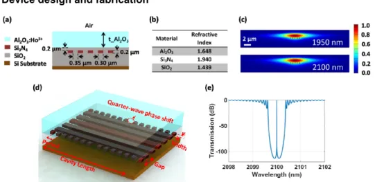
2. Device design and fabrication
Fig. 1. (a) Cross-sectional view of the laser waveguide including five strips of Si3N4, an
Al2O3:Ho3+ film, SiO2 and air as a lower and upper cladding, respectively on Si substrate. (b)
Refractive indices of the waveguide materials. (c) Transverse-electric (TE) field intensity for the fundamental mode at the pump (1950 nm) and laser output (2100 nm) wavelengths in the DFB waveguide. (d) 3D illustration of the DFB laser showing the different material layers and cavity features (not to scale). (e) Calculated transmission of designed DFB cavity at 2100 nm.
The waveguide cross-section of the DFB laser is shown in Fig. 1(a). A wavelength-insensitive waveguide design is used, which exhibits a high confinement factor in the gain material for an octave-spanning range across near-IR wavelengths (950-2000 nm) [45]. The octave-spanning range enables the waveguide structure to be used for a broad selection of pump and lasing wavelength. It consists of five Si3N4 bars buried under SiO2 with a layer of Al2O3:Ho3+
deposited on top. The thickness of each Si3N4 bar is 200 nm, and the oxide gap between this
Si3N4 layer and the Al2O3 layer is 200 nm. The width and separation of the Si3N4 bars are
optimized to be 300 nm and 350 nm, respectively, to provide high mode confinements for both pump (1.95 μm) and signal modes (~2.10 μm) within the Al2O3:Ho3+ film. Using a
vector finite-difference 2D eigenmode solver, the confinement factors within the holmium-doped gain region for pump and signal are calculated to be 85% and 83%, respectively.
The refractive indices of the materials used in our laser design are listed in Fig. 1(b). At both pump and signal wavelength, the refractive indices are sufficiently close that the material dispersion is negligible and excluded from the calculations. The guided modes in waveguides and the effective indices are calculated by vector finite-difference 2D eigenmode solver, with a discretization of 20 nm. The code is written in Matlab, and it solves the wave equation of the transverse electric field. After solving the eigen problem, the square of propagation constant β2 can be obtained as eigenvalue, and hence the effective index was calculated using
neff = βλ/2π. The transverse-electric (TE) field intensity of the fundamental mode at the pump
and signal wavelengths is shown in Fig. 1(c).
A perspective view of the DFB laser is illustrated in Fig. 1(d) showing the perturbations on the side of the waveguide to form the laser cavity. The lateral gap between the grating and waveguide is designed to be 450 nm, and the grating width is chosen to be 260 nm in order to provide enough feedback at the designed laser wavelength. The coupling coefficient (κ) of Bragg grating is calculated to be 1.10 × 10³ m−1, by substituting the calculated β from mode
solver into the following Eq [46]:
3 4 2 2 2 2 ( )sin( ) 2 Si N SiO k n n D κ π τ πβ = − (1)
where D is grating duty cycle, which is equal to 0.5,
τ
is the mode overlap within the grating region, which is calculated to be 0.21%, k is the wave number. The refractive index of nSi3N4and nSiO2 are provided in Fig. 1(b). The total length of the cavity is 2 cm, which is limited by
the length of the chip from fabrication facility. For a laser cavity length shorter than 2 cm, with the same pump power, the lasing power decreases. The mask space available for Holmium doped lasers on this fabrication run was limited to 2 cm × 0.05 cm. With a larger area available, a longer laser cavity (>2 cm) can be designed using a spiral geometry [36] for higher gain and better laser performance in terms of slope efficiency, output power and lasing threshold. The effective index (neff) of the waveguide is calculated to be 1.552 at 2100 nm,
considering the grating as perturbations on both sides of the segmented Si3N4-rib to provide
feedback. Therefore, the grating period (ᴧ) can be calculated using:
2neff
λ
Λ = (2)
where λ is the designed laser wavelength. Based on the neff from 2D mode solver and κ
obtained from Eq. (1) above, the transmission response of our DFB cavity, as shown in Fig. 1(e), is calculated by using the transfer matrix of grating [46]. A quarter-wave phase shift is introduced in the middle of the simulated section, with κ reversing sign: κ = - κ.
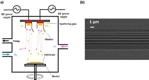
The lasers were fabricated in a state-of-the-art CMOS foundry on a 300-mm silicon wafer. The wafer-scale fabrication process before the Al2O3:Ho3+ film deposition is the same as that
which has been reported earlier [44]. After dicing the wafer into small identical chips, a 1.14-µm-thick Al2O3:Ho3+ film was deposited on one of the chips via reactive co-sputtering as a
back-end-of-line process. The doped Al2O3 film was reactively co-sputtered from 2-inch
diameter metallic aluminum and holmium targets in a confocal arrangement. The reaction was within an argon and oxygen atmosphere. The deposition system (AJA ATC Orion 5), as shown in Fig. 2(a) below, is equipped with two radio frequency (RF) magnetron sputtering guns. The power setting on the aluminum and holmium sputtering guns were 200 W and 18 W, respectively. The deposition was carried out at a constant pressure of 3 mTorr. The argon flow rate was kept at constant flow of 11.0 sccm, and the oxygen flow rate was adjusted from 1.1 to 1.6 sccm in order to maintain the oxygen flow – bias voltage curve at the “knee” point of the hysteresis point [47] during the entire deposition process. At this point, the film deposited is stoichiometric, while the oxygen flow is maintained below the point where the bias voltage of aluminum target and deposition rate start to drop. The substrate temperature was measured to be 415 °C. Deposition runs with different Ho3+ doping levels revealed that a
measured Ho3+ doping concentration of 3.2 × 1020 cm−3, through Rutherford backscattering
spectrometry (RBS) analysis, provides the best lasing performance. Given the same pump power, a lower doping concentration will suffer from lower gain while higher doping concentration will result in ion clustering or quenching [48–50]. In addition, the propagation loss of the passive Al2O3 film (without doping) deposited on a thermally oxidized silicon
substrate was measured using the prism coupling method. The propagation loss of the Al2O3
film was found to be < 0.1 dB/cm.
A scanning electron microscopy (SEM) image of Si3N4 layer is illustrated in Fig. 2(b). In
order to remove the top SiO2 cladding layer for SEM imaging, prior to Al2O3 deposition, the
device was placed into buffered hydrogen fluoride (HF) for 140 s and coated with 5 nm thin gold layer at top to avoid charging.
Fig. 2. (a) Schematic diagram of reactive sputtering deposition system: two guns with RF power supply are mounted at the top of the chamber. Ar3+ ions are accelerated to bombard the
Al and Ho targets. O2 is supplied for reaction. The Al2O3:Ho3+ film is formed on substrate,
which is heated up by heater from bottom of the chamber. (b) SEM image of the Si3N4 pattern
(top view) after removing SiO2 top cladding by hydrogen fluoride (HF) etching.
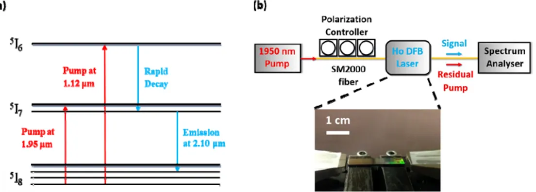
3. Device characterization
The common pumping scheme of holmium is shown in Fig. 3(a). For direct pumping of singly-doped holmium, the absorption bands of interest lie at wavelengths of 1.15 μm (4I
7
level) and 1.95 μm (5I
7 level). Pumping of the 4I7 level can be addressed by 1.12 μm laser
diodes [8] or long wavelength operation of ytterbium fiber lasers [51]. However, the low quantum efficiency of this pumping scheme limits its efficiency and power scaling potential. Alternatively, the 5I
7 level can be accessed by thulium fiber or on-chip lasers, which can
provide a high-power pump source at 1.95 μm.
The measurement setup for characterization of the lasers is illustrated in Fig. 3(b). A high-power fiber laser source at 1950 nm was used for optical pumping. A polarization controller was used to ensure that the pump light is coupled into the fundamental TE mode of the gain waveguide. A cleaved single-mode SM-2000 fiber was used to butt-couple the pump light onto the chip, and another cleaved single-mode SM-2000 fiber was used to butt-couple the output signal of the laser from the chip. The setup and fiber-to-chip coupling losses were first determined using a 3-mm-long passive waveguide, which had an undoped Al2O3 film at top
but was otherwise identical to the laser gain waveguide, and SM-2000 fibers on each side of the chip for both pump and lasing wavelengths. The fiber-to-chip coupling losses for SM-2000 were measured to be 7.5 dB at the pump wavelength, and 6.9 dB at the laser output wavelength. The output signal was coupled into an optical spectrum analyzer (Yokogawa AQ6375) to capture the spectrum.
Fig. 3. (a) 3-level holmium laser energy diagram showing pump and laser transitions. (b) The measurement setup, which contained a high-power 1950 nm thulium fiber laser as pump source, a polarization controller for efficient coupling, and an optical spectrum analyzer to capture the output spectrum. Cleaved fibers are used to butt couple pump and signal onto or from the chip.
Fig. 4. Broadband spontaneous emission of (a) Al2O3:Tm3+ film covering from 1680 nm to
2020 nm, pumped by a low power 1614 nm pump source and (b) Al2O3:Ho3+ film covering
from 1930 nm to 2130 nm, pumped by a 1120 nm pump source.
First, we compare the spontaneous emission spectra of thulium- and holmium-doped Al2O3 films, which both emit near 2 µm. We deposited Al2O3:Tm3+ and Al2O3:Ho3+ films on
top of the Si3N4 waveguide design illustrated in Fig. 1(a). A low power pump at 1.614 μm (at
the Tm3+ absorption peak) was used to generate spontaneous emission in the Al
2O3:Tm3+
waveguide on the 3F
4 →3H6 transition. The spectrum recorded by an optical spectrum
analyzer is shown in Fig. 4(a). It shows that the emission range is from 1680 nm up to 2020 nm, with 3-dB bandwidth of 340 nm. Lasing within this emission range has been reported by using the same Al2O3:Tm3+ thin film and varying the grating period [44]. In comparison, the
spontaneous emission spectrum of the Al2O3:Ho3+ film is shown in Fig. 4(b). A low power
laser source at 1.12 μm is used as the pump. The emission range has a 3-dB bandwidth of 200 nm, spanning from 1930 nm up to 2130 nm, which is beyond the upper limit of the Al2O3:Tm3+ emission. Lasing within this emission range is achieved by varying the grating
period as well as Al2O3 thin film thickness, as shown in the following parts of this article.
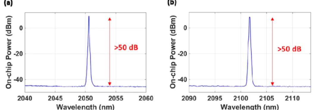
To demonstrate lasing using Al2O3:Ho3+ as a gain medium, two DFB lasers with different
grating periods were fabricated. The two grating periods were 659 nm and 677 nm, which based on Eq. (2), correspond to wavelengths around 2051 nm and 2101 nm, respectively. The measured optical spectra of the corresponding DFB laser designs are shown in Figs. 5(a) and 5(b). Due to the narrow reflection bandwidth of the DFB structure, single-mode operation is demonstrated and more than 50 dB side-mode suppression ratio is achieved for both designs. A 50 pm (~3.4 GHz) optical spectrum analyzer resolution used in the experiment confirms the single mode operation of the laser with ~5 GHz free spectral range. Within the broad gain
bandwidth of Al2O3:Ho3+, we are able to control the laser wavelength by choosing a proper
grating period based on Eq. (2).
Fig. 5. The output spectra of the DFB lasers at (a) 2051 nm and (b) 2101 nm obtained with up to 800 mW on-chip pump power, showing side-mode suppression ratios >50 dB.
Fig. 6. (a) DFB laser output power with respect to on-chip pump power: showing 2% slope efficiency, 130 mW lasing threshold and 15 mW maximum output power; (b) DFB laser output power with respect to absorbed pump power near the lasing threshold: showing 50 mW lasing threshold and 2.3% slope efficiency.
The device that operates at the higher emission cross-section of the holmium gain spectrum, which is 2050 nm, was selected for the lasing slope efficiency measurement shown in Fig. 6. The maximum on-chip output power of the DFB laser was measured to be 15 mW, limited by the on-chip pump power of 800 mW. The output power was measured from a single side of the laser and the fiber-to-chip coupling loss was calibrated out. An equivalent level of power can be obtained if the pump is launched from the other side of the laser due to the symmetry of the cavity design. Using linear curve fitting to the experimental data, we demonstrate a single-sided slope efficiency of 2.0% and a laser threshold of 130 mW with 1950 nm pumping. In order to find the effective lasing threshold with respect to absorbed pump power, the residual pump power was measured near the lasing threshold of the same device. The absorbed pump power is obtained by subtracting the measured residual pump from the on-chip pump power. The laser power near the threshold with respect to absorbed pump power is shown in Fig. 6(b). The lasing threshold with respect to absorbed pump power is found to be 50 mW, and the slope efficiency is measured to be 2.3%, after linear curve fitting of experimental data. The slope efficiency reported here is limited by the loss in the laser cavity, which is mainly attributed to the waveguide surface roughness and loss from the materials (Si3N4, Al2O3, SiO2). The loss of the laser cavity can be reduced by improving
fabrication process (e.g. using LPCVD instead of PECVD Si3N4). In addition, the laser
by using a distributed-phase-shifted (DPS)-DFB with optimized grating coupling coefficient (κ) instead of a quarter-wave phase shift (QPS)-DFB [45]. The improvement of the DPS-DFB cavity can be attributed to the reduction of spatial hole burning in QPS-DFB cavity and a longer effective gain section.
4. Lasing wavelength shift by changing Al2O3:Ho3+ film thickness
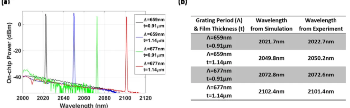
Since the deposition of the Al2O3:Ho3+ thin film is a back-end-of-line process, the lasing
wavelength of our DFB laser can be controlled by changing the thickness of the film. Using the same Si3N4 grating periods (659 nm and 677 nm), the thickness of the film is reduced
from 1.14 μm to 0.91 μm by reducing the sputtering time in a new Al2O3:Ho3+ deposition run.
The lasing wavelength is shifted from 2050.2 nm to 2022.7 nm and 2101.4 nm to 2072.6 nm, respectively, as shown in Fig. 7(a) below. In addition, the effective index of the gain waveguide with reduced Al2O3:Ho3+ film thickness is calculated using the 2D eigenmode
solver, and hence the expected lasing wavelengths are calculated by substituting the neff and
grating period into Eq. (2). A comparison of the calculated lasing wavelength from simulation and the measured lasing wavelength from the experiment is shown in Fig. 7(b). They agree to an accuracy of 1 nm. The difference may be caused by fabrication variation of the Si3N4
layer, as well as by the Al2O3:Ho3+ film thickness non-uniformity along the 2-cm-long DFB
cavity [52]. In addition, the thermal shift of the device, which was reported to be 0.02 nm/°C [42], may also have an effect.
Lasing was observed with film thicknesses ranging from 0.85 μm up to 1.25 μm. If the film thickness is less than 0.85 μm, the laser device experiences low gain. This is due to the fact that as the film gets thinner, the pump and signal mode overlap decreases, and therefore the gain decreases. Meanwhile, if the film thickness is more than 1.25 μm, the laser device experiences high round-trip loss. This is mainly due to the fact that as the film gets thicker, the horizontal mode confinement (provided by Si3N4 bars) is weaker and hence the expanded
mode will experience more scattering loss. Additionally, with a gain film thickness in the range of 0.85 μm to 1.25 μm, there is an optimum thickness value to provide the highest net gain giving the best laser performance in terms of output power, slope efficiency and lasing threshold.
Fig. 7. (a) Demonstration of lasing wavelength control by changing the gain film thickness. (b) Comparison of calculated lasing wavelength from simulation and real lasing wavelength from experiment.
5. Conclusion
In summary, we have designed, fabricated and characterized holmium doped DFB lasers monolithically integrated on a silicon chip. The holmium-doped Al2O3 glass, which provides
broadband emission from 1930 nm to 2130 nm, was used as gain medium. A CMOS-compatible segmented Si3N4 rib-waveguide was used to form the laser cavity. Gratings were
the grating period, we demonstrated single-mode lasers with wavelengths at 2051 nm and 2101 nm, which are within the holmium gain bandwidth. By changing the Al2O3:Ho3+ film
thickness, the lasing wavelength can be controlled. With 1950 nm pumping, a laser output power of 15 mW was measured at a wavelength of 2050 nm with a slope efficiency of 2% and greater than 50 dB side-mode suppression ratio. This demonstration represents an important step toward high-performance on-chip silicon-based laser sources for the 2 to 2.2 µm wavelength range.
Funding
Defense Advanced Research Projects Agency (DARPA) E-PHI project (grant no. HR0011-12-2-0007); Defense Advanced Research Projects Agency (DARPA) DODOS project (grant no. HR0011-15-C-0056).
Acknowledgment
The authors would like to acknowledge Professor Federico Capasso and Professor Franz Kärtner for helpful discussion, Gary Riggott and Kurt Broderick for assistance on holmium doped thin film deposition, and Di Zhu for assistance with SEM imaging. N. Li acknowledges a fellowship from the Agency of Science, Technology and Research (A*STAR), Singapore.