RESEARCH OUTPUTS / RÉSULTATS DE RECHERCHE
Author(s) - Auteur(s) :
Publication date - Date de publication :
Permanent link - Permalien :
Rights / License - Licence de droit d’auteur :
Institutional Repository - Research Portal
Dépôt Institutionnel - Portail de la Recherche
researchportal.unamur.be
University of Namur
Probing the growth window of LaVO3 perovskites thin films elaborated using
magnetron co-sputtering
Celindano, Christophe; Haye, Emile; Bruyère, Stéphanie; Boulet, Pascal; Boileau, Alexis;
Migot, Sylvie; Mathieu, Sandrine; Miska, Patrice; Barrat, Silvère; Capon, Fabien
Published in: Ceramics International DOI: 10.1016/j.ceramint.2019.05.208 Publication date: 2019 Document Version
Peer reviewed version
Link to publication
Citation for pulished version (HARVARD):
Celindano, C, Haye, E, Bruyère, S, Boulet, P, Boileau, A, Migot, S, Mathieu, S, Miska, P, Barrat, S & Capon, F 2019, 'Probing the growth window of LaVO3 perovskites thin films elaborated using magnetron co-sputtering',
Ceramics International, vol. 45, no. 13, pp. 16658-16665. https://doi.org/10.1016/j.ceramint.2019.05.208
General rights
Copyright and moral rights for the publications made accessible in the public portal are retained by the authors and/or other copyright owners and it is a condition of accessing publications that users recognise and abide by the legal requirements associated with these rights. • Users may download and print one copy of any publication from the public portal for the purpose of private study or research. • You may not further distribute the material or use it for any profit-making activity or commercial gain
• You may freely distribute the URL identifying the publication in the public portal ?
Take down policy
If you believe that this document breaches copyright please contact us providing details, and we will remove access to the work immediately and investigate your claim.
Probing the growth window of LaVO
3perovskites thin films
elaborated using magnetron co-sputtering
Christophe Celindanoa,∗, Emile Hayeb, St´ephanie Bruy`erea, Pascal Bouleta, Alexis Boileauc,
Sylvie Migota, Sandrine Mathieua, Patrice Miskaa, Silv`ere Barrata, Fabien Capona
aUniversit´e de Lorraine, IJL, CNRS, F-54000 Nancy, France
bLaboratoire Interdisciplinaire de Spectroscopie Electronique (LISE), Namur Institute of Structured Matter
(NISM), University of Namur, 61 Rue de Bruxelles, 5000 Namur, Belgium
cCRISMAT, CNRS UMR6508, ENSICAEN, Normandie Universit´e, 14050 Caen Cedex 4, France
Abstract
LaVO3 is a promising material for tuning and improving solar cell performances when modifying
the La/V stoichiometry. However, the production of LaVO3 thin films still requires a complex
process (MBE, PLD), and the growth window of LaVO3structure in terms of La/V ratio, already
defined in the literature using hybrid-MBE is not determined for elaboration based on magnetron co-sputtering of both vanadium and lanthanum targets followed by an external reducing annealing that we use here. La/V ratio has been varied from 0.52 to 1.68 by changing the power applied to the vanadium target in order to synthesize films with different La/V ratios. The off-stoichiometry growth window has been investigated by complementary methods (XRD, XPS, FTIR and TEM). X-ray diffraction highlights the LaVO3 structure for all the films. For La-rich samples (La/V ratio
> 1.2), the formation of lanthanum oxide La2O3 is observed at the top surface and interface with
the substrate, according to XPS, FTIR and TEM investigations. On the other hand, for V-rich samples, only a slight modification of the structure is observed below the La/V ratio = 0.6; with the presence of a new IR vibration mode corresponding to a small contribution of vanadium oxide(s) present in volume. Our study allows a better definition of the LaVO3 growth window in terms of
La/V ratio, estimated from 0.6 to 1.2.
Keywords: Oxide, Thin film, Sputtering, Crystallization, Vanadate, Perovskite
Declarations of interest: none
∗Corresponding author
Email address: [email protected] (Christophe Celindano)
Preprint submitted to Ceramics International May 6, 2019
Version of Record: https://www.sciencedirect.com/science/article/pii/S0272884219313215
1. Introduction
The conventional solar cells have a limited energy conversion efficiency because photons with energies lower than the band gap are not absorbed and those with higher energies mainly produce phonons. One of the possible ways to circumvent this problem is the use of multi-junctions with
5
several layers that cover a larger part of the solar spectrum. In this way, Mott insulators as solar-absorbers using carrier multiplication could be considered [1]. Indeed, lanthanum vanadate LaVO3
is a promising candidate with an indirect forbidden band gap close to 1.1 eV [2], i.e. close to the ShockleyQueisser limit [3] and a good absorption coefficient [4]. This perovskite material and more especially the off-stoichiometry La1+xVO3 films have already been studied for photovoltaic 10
solar applications [5, 6] but mainly by a hybrid molecular beam epitaxy growth method. In such an approach, the authors investigated the off-stoichiometry LaVO3 samples by varying La/V ratio
during the synthesis. However, most of the studies deal with lanthanum over-stoichiometry, in a small range of concentration. The effect of La/V ratio variation over a wide range in LaVO3remains
an open question.
15
Usually, lanthanum vanadate films are deposited by pulsed laser deposition, molecular beam epitaxy or are synthesized through powder reactions of lanthanum and vanadium oxides [7, 8, 9, 10, 11, 12]. These growth processes are limited in terms of upscaling concerns. Therefore, by focusing here on the sputtering technique, we use an alternative way for the synthesis of crystalline LaVO3.
The synthesis is based on a two-step process with 1) deposition of a LaVO thin-film by magnetron
20
co-sputtering and 2) ex-situ annealing under a reducing atmosphere. Such a process is easy to up-scale for large surfaces treatments as required for many industrial applications.
For possible use in photovoltaics, the goal of the present paper is to extend the present knowledge about the growth of LaVO3 using magnetron sputtering, particularly by determining LaVO3growth
window where no formation of additional phases is observed. In this view, thin films with different
25
La/V atomic ratios (from 0.52 to 1.68) are obtained adapting the sputtering electrical parameters and analyzed using X-ray diffraction (XRD), X-ray photoelectron spectroscopy (XPS), transmission electron microscope (TEM) and infrared spectroscopy.
2. Experimental section
LaxVyO3 thin films deposited on double side polished silicon substrates are grown using a 30 30
L sputtering chamber connected to a turbomolecular secondary pump backed by a rotary pump to get a vacuum close to 5 · 10−5 Pa before each deposition process. Two inches diameter lanthanum and vanadium targets with atomic purity of 99.9% are used for the co-sputtering. The targets are surrounded by plasma suppressors and separated by a distance of 80 mm, long enough to avoid any observable plasma interaction between the two targets during the process. Substrates are mounted
35
on a rotating holder and located at 55 mm and 70 mm away from respectively the lanthanum and vanadium targets. Discharge parameters have been optimized from previous works using similar elements [13, 14, 15, 16, 17, 18]. The lanthanum target is powered by an Advanced Energy Pinnacle 5kW pulsed-DC generator under a power regulation of 75 W, a frequency of 100 kHz and an off-time of 4 µs while vanadium target is powered by an Advanced Energy MDX 500W DC generator with
40
a pre-chosen and fixed power ranging from 200 to 300 W. The pressure control is established by using an MKS Baratron 627 capacitive gage with a 1.33 hPa range and the gas are flown (at 21 sccm for argon and varying flow for the oxygen) using Alphagaz RDM 280 flowmeters. Substrates temperature is evaluated by using a thermocouple, located inside the substrates holder.
Prior to the deposition, the substrates used are cleaned with acetone and ethanol, followed by
in-45
situ by reactive-ion etching (RIE) with an Advanced Energy Cesar radiofrequency (RF) generator inside the sputtering chamber for 5 minutes under gas flows close to the growth conditions (i.e. under 21 sccm of Ar and 7 sccm of O2).
Two types of annealing treatments have been tested to crystallize the perovskite, namely an air annealing and a reducing annealing. The first annealing is carried out in the air and performed with
50
a Barnstead type 47900 furnace at 900◦C for 5 min. For the second annealing, a homemade furnace is used for the post-growth annealing step, composed of a quartz cylinder receiving a sample-holder where a primary vacuum is done before the heating step. The annealing temperature is regulated with an Eurotherm temperature regulator while the gas flows are controlled via a MKS Type 647C controller. The sample-holder is a quartz semi-cylinder previously cleaned with acetone and ethanol
55
before each use. in a gaseous mixture of 90% Ar and 10% H2 working pressure is fixed at 700 torr
and a temperature ramp has been fixed, with a temperature of 900◦C, reached in 90 min and kept constant for 60 min. When the cycle ends, gas flows are set to zero and the quartz chamber is isolated, with a static pressure imposed by the amount of remaining gas. Samples are then cooled
to ambient temperature in almost six or seven hours.
60
FEI/Philips XL-30 field emission environmental scanning electron microscope (ESEM) working at 15 kV provides X-ray energy dispersive spectroscopy (EDS) measurements, useful for the La/V atomic ratio estimation of the different samples with a thickness varying between 200 and 300 nm. Analyzing thin films, the composition estimation is reliable for studying an atomic ratio evolution, not in absolute value.
65
The chemical composition of the LaxVyO3 thin films have been investigated by XPS (K-Alpha
Thermo Scientific spectrometer) using a monochromatic Al K alpha radiation (1486.68 eV). The X-rays spot size was 250 µm in diameter. Spectra (La 3d, O 1s and V 2p) have been recorded with an energy resolution of 0.5 eV and a pass energy of 20 eV. The number of scans was adjusted (between 5 and 30 scans) for each element to get similar signal-to-noise ratios. A flood gun was
70
used for the charge compensation and spectra were calibrated by fixing the La 3d 5/2 main peak at 833.6 eV, as the intensity of the adventitious carbon peak was too weak, and the La 3d 5/2 peak does not exhibit significant shift [19]. Peak-fitting was performed with the Avantage software (Thermo Scientific).
The structure of the sample is investigated by XRD with a Brucker D8 Advance diffractometer
75
(λCuKα1= 1.54056 ˚A) using the Bragg-Brentano θ − 2θ configuration.
A doubly corrected JEOL ACCEL ARM Cold FEG 200F TEM coupled with a GATAN GIF Quantum ER was used in scanning transmission electronic microscopy (STEM) mode for Electron Energy Loss Spectroscopy (EELS) measurements (energy dispersion of 0.1 eV/channel, a full width at half maximum (FWHM) of 0.6 eV, a 2 nm pixelsize and a pixeltime of 0.5 s/pixel to avoid
80
beam damage). Fast Fourier transform (FFT) of high resolution transmission electron microscopy (HRTEM) images were recorded to obtain the crystallographic structure. Thin foils of selected samples were prepared by the focused ion beam (FIB) technique using a FEI HELIOS NanoLab 600i FIB/SEM.
3. Results and discussion
85
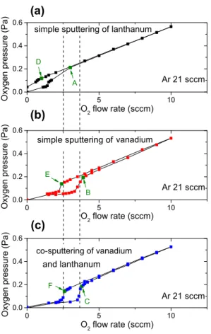
3.1. Discharge characteristic
The sputtering of lanthanum and vanadium in the presence of a reactive atmosphere has been investigated using hysteresis experiments, by sputtering each target separately or simultaneously.
The parameters used are the further deposition parameters given in the table 1 except that for the hysteresis study we use a fixed power of 250 W applied to the vanadium target and a variable
90
O2 flow rate. Before the hysteresis experiments, targets are sputtered in pure Ar gas for half an
hour using the previous given parameters in order to avoid residual oxides and start the hysteresis experiments with metallic elements.
Figure 1 shows the oxygen partial pressure behavior as a function of the O2flow rate using single
sputtering (targets sputtered separately, Figure 1.a and 1.b) and the co-sputtering (Figures 1.c).
95
The oxygen partial pressure is obtained by making the difference of total pressures measured with or without oxygen. In the absence of oxygen, pure metallic atoms are sputtered from the targets, which is often called the elemental sputtering mode (ESM) [20]. When oxygen is introduced in the chamber, this leads to a target poisoning caused by both chemisorption and ion implantation of oxygen molecules [21]. In the case of the lanthanum we could consider that the target surface is
100
fully covered by an oxide layer when the oxygen pressure starts to increase linearly with the O2
flow rate i.e. around 2 sccm O2 flow rate (see point A in Figure 1) leading to a regime where only
compounds are sputtered and called reactive sputtering mode (RSM). For the vanadium target the transition occurs for an O2 flow rate higher than 4 sccm (see point B in Figure 1.b) then, taken
separately, the lanthanum is more reactive in an oxygen atmosphere than the vanadium.
105
When targets are sputtered together, the hysteresis curve (see point C Figure 1.c) is very similar to the vanadium one indicating that the simultaneous sputtering is driven by the vanadium element because even more reactive, the lanthanum target is still sputtered in ESM until the vanadium target becomes fully oxidized on the surface and then both targets are sputtered in RSM. At 10 sccm, the O2 flow rate is slowly decreased to zero (backward direction of the hysteresis) but the RSM is 110
still effective for 02 flow rates lower than before for simple and co-sputtering (see points D, E and
F in Figure 1). This could be explained by the fact that despite the reduction of oxygen content, targets are still oxidized and become metallic only for smaller O2flow rates.
Further, this result implies that changing the deposition parameters is more efficient by modi-fying the vanadium parameters than the lanthanum ones. Next, the choice is made to change the
115
0 5 10 0.0 0.2 0.4 0.6 0 5 10 0.0 0.2 0.4 0.6 0 5 10 0.0 0.2 0.4 0.6 B D Ar 21 sccm simple sputtering of lanthanum
O xyg e n p r e ssu r e ( P a ) O 2 flow rate (sccm) (c) A C E Ar 21 sccm O xyg e n p r e ssu r e ( P a ) O 2 flow rate (sccm) simple sputtering of vanadium
F O xyg e n p r e ssu r e ( P a ) O 2 flow rate (sccm) Ar 21 sccm (a) (b) co-sputtering of vanadium and lanthanum
Figure 1: Oxygen partial pressure vs the oxygen flow rate of the hysteresis experiment for the sputtering of (a) the lanthanum target, (b) the vanadium target and (c) both targets together.
3.2. Elaboration and annealing of LaxVyO3 thin films
The deposition parameters are given in table 1. The discharge power applied to the vanadium target is changed from 200 to 300 W inducing the modification of the La/V ratio.
As-deposited thin films are amorphous as observed by XRD in Figure 2. An annealing step is
120
necessary to crystallize the perovskite-phase [22]. We first used an annealing made under air at 900◦C for 5 min inducing the formation of LaVO4 structure (Figure 2), where the vanadium has
Table 1: Experimental parameters for the elaboration of the samples by magnetron sputtering
Parameter value unit
Ar flow 21 sccm O flow 7 sccm Working pressure 1.5 Pa PV (DC) variable W V target distance 7 cm PLa (DC-pulsed) 75 W fLa 100 kHz ToffLa 4 µs La target distance 5.5 cm Substrates temperature ≈ 60 ◦C
requires a post-growth annealing treatment under an Ar/H2 (100/10 sccm respectively ) reducing
atmosphere. 125 20 30 40 50 60 70 80 ( 1 2 1 )
sample annealed at ambient atmosphere
LaVO 4 I n t e n s i t y ( a . u ) 2 (°) LaVO 3 amorphous
sample annealed in a mix of Ar/H 2 as-deposited film ( 1 2 0 )
Figure 2: Diffractograms for a sample with a La/v ratio close to 1. As deposited film is amorphous whereas an ex-situ annealing leads to LaVO4or LaVO3 depending on the annealing atmosphere (air or Ar/H2 mixture).
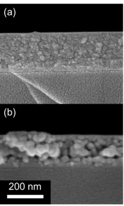
The air annealing is then replaced by a reducing annealing process, performed under pumping while injecting Ar/H2 gas mixture. For all samples, SEM cross-sections performed on both
pre-and post-annealed steps (see Figure 3) show a morphological modification, from dense (for an as-deposited sample in Figure 3.a) to porous (after annealing in Figure 3.b) reducing the thickness of
almost twenty percents. This density drop i.e. porosity increase can be explained by the oxygen
130
losses during the annealing.
Figure 3: Layer morphology observed with the SEM high-resolution mode in cross-section at a working distance of 5 mm, for a 3 kV acceleration voltage and a 200k magnification. The La/V ratio is around 1.68 in this case. Micrograph (a) shows cross-section of the as-deposited film and (b) after the reducing annealing.
3.3. Growth window of LaVO3
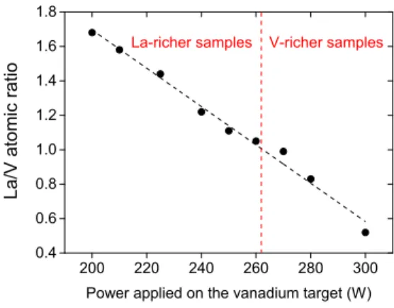
La/V atomic ratio, evaluated by EDS measurement and which is not varying with the reducing annealing step, exhibits a linear evolution as a function of the discharge power applied to the vanadium target (see Figure 4).
135
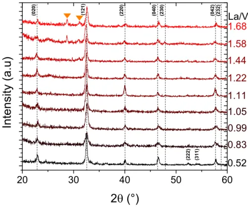
Figure 5 shows the diffractograms from XRD measurements after reducing annealing. All the films present LaVO3 orthorhombic structure [23] with the space group Pnma (62). Beyond the
La/V value of 1.22, a crystallized La2O3 cubic phase [24] appears in addition to the orthorhombic
200 220 240 260 280 300 0.4 0.6 0.8 1.0 1.2 1.4 1.6 1.8 L a / V a t o m i c r a t i o
Power applied on the vanadium target (W )
La-richer samples V-richer samples
Figure 4: Evolution of the La/V atomic ratio (estimated using EDS) varying the power applied on the vanadium target. Power on the lanthanum target is kept constant and other parameters are given in table 1.
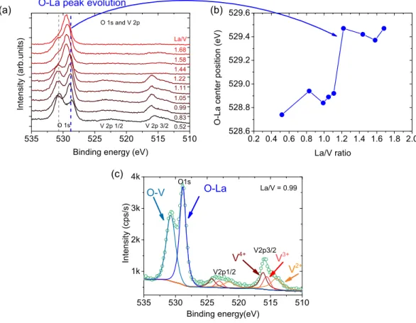
To obtain more information about the chemical composition, XPS Spectra were recorded
be-140
tween 510 and 535 eV and are reported in Figure 6.a in order to obtain both O 1s and V 2p core levels for the different La/V ratios. As the O 1s and V 2p levels are near, they have been recorded and fitted with a unique background, as suggested by Biesinger [25]. The peak fitting is shown in Figure 6.c: O 1s signal presents two contributions, centered at 528.8 and 530.7 eV, corresponding to O-La and O-V binding energies respectively. The V 2p signal exhibits two peaks corresponding
145
to 3/2 and 1/2 spin-orbit splitting, with an energy difference of 7.5 eV. It appears that several contributions have to be used to fit these peaks, indicating different oxidation states of vanadium as previously reported [26, 27]. Three contributions have been used for the V 2p3/2 peak fitting, centered at 514.1, 515.6 and 516.2 eV, that corresponds to +II, +III and +IV vanadium oxidation states. As La/V ratio increases, two major effects occur. First, the O-V binding contribution
ex-150
tinguishes (see Figure 6.a) due to the lower concentration of vanadium at the surface. Contrary to previous works dealing with LaVO3elaborated by PLD [27, 28, 29], the O-V binding contribution
to the O 1s level compared to the O-La one seems to be higher, which could be explained by the possible presence of vanadium oxides VOxat least at the surface of the V-richer samples. The effect
is predominant from a ratio of 1.22. Secondly, a shift from 528.8 to 529.4 eV of the O-La
contri-155
bution is observed for ratios higher than 1.22 (Figure 6.a and 6.b). This difference is attributed to the presence of La2O3 which appears with this high ratio as confirmed by XRD measurements
20 30 40 50 60 ( 3 1 1 ) ( 2 2 2 ) ( 0 4 2 ) ( 2 3 2 ) ( 2 3 0 ) ( 0 4 0 ) ( 2 2 0 ) ( 1 2 1 ) 0.52 0.83 0.99 1.05 1.11 1.22 1.44 1.68 I n t e n s i t y ( a . u ) 2 (°) La/V 1.58 ( 0 2 0 )
Figure 5: X-ray diffractogram in 2θ geometry of samples elaborated for different La/V atomic ratio. Two new peaks are appearing with the lanthanum richer samples (see the two orange triangles) which can be attributed to the La2O3cubic structure.
not associated with a variation of the La-O coordination among the LaVO3 perovskite phase. The
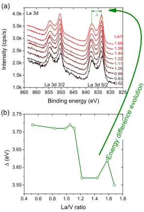
signal corresponding to the perovskite phase is shifted around 0.6 eV compared to La2O3. 160
The evolution of the La 3d signal for the different La/V ratios is reported in Figure 7.a. The signal exhibits a doublet due to the splitting of La 3d into 5/2 and 3/2 contributions. Then, a second multiplet splitting is observed in each contribution, that is attributed to the interatomic charge transfer of the O 2p to La 4f level, by the shake-up process, that ends in 3d9f1 final state
[30, 31]. The delta between these two contributions (main peak and satellite) is widely dependent
165
on the species, and may vary in a wide range (from 3.37 to 4.27 eV, see [32]), while the main peak position is only slightly affected [33]. The plot of the energy difference ∆E between the main contribution of La 3d5/2, centered at 833.6eV, and its satellite is shown in Figure 7.b. The evolution
535 530 525 520 515 510 0.2 0.4 0.6 0.8 1.0 1.2 1.4 1.6 1.8 2.0 528.6 528.8 529.0 529.2 529.4 529.6 535 530 525 520 515 510 1k 2k 3k 4k (a) V 2p 3/2 V 2p 1/2 O 1s O 1s and V 2p 1.68 1.58 1.44 1.22 1.11 1.05 0.99 0.83 I n t e n si t y ( a r b . u n i t s)
Binding energy (eV)
0.52 La/V O -L a ce n t e r p o si t i o n ( e V ) La/V ratio (b)
O-La peak evolution
O1s V2p3/2 (c) I n t e n si t y ( cp s/ s) O-V O-La V 2+ V 3+ Binding energy(eV) V 4+ La/V = 0.99 V2p1/2
Figure 6: O1s and V2p core level spectra for sample with different La/V ratio (a). Evolution of the O-La binding energy as a function of the different La/V ratio (b). Example of peak fitting with the six contributions of V2p signal and the two contribution of O1s signal (c).
confirms the previous observation, with a drop of ∆E from 3.71 to 3.57 eV, when the atomic ratio reach 1.22 or higher values. As previously, this drop is attributed to the apparition of La2O3. 170
In order to see the effect of the La/V ratio variation, cell parameters refinements were performed (Fullprof Suite). Figure 8 presents the cell-volume evolution with the La/V ratio obtained after the refinement (varying from 233 to 241 ˚A3 with an error of almost 4 ˚A3). The refined volume
does not evolve with this two-step synthesis in opposition to films obtained by molecular beam epitaxy [6] where the out-of-place parameter decreases when La/V ratio differs from one. In our
175
case, this means that all the lanthanum in excess introduced in the lanthanum-richer samples is not incorporated in the LaVO3 phase but in the La2O3 phase. The mean cell-volume value is 240 ˚A3
0.4 0.6 0.8 1.0 1.2 1.4 1.6 1.8 3.55 3.60 3.65 3.70 3.75 (b) La/V ratio ( e V ) 865 860 855 850 845 840 835 830 825 1.0k 1.5k 2.0k 2.5k 3.0k 3.5k 4.0k (a) La 3d 3/2 La 3d 5/2 I n t e n s i t y ( c p s / s )
Binding energy (eV)
0.52 0.83 0.99 1.05 1.11 1.22 1.44 1.58 1.68 La/V La 3d E n e r g y d i f f e r e n ce e vo l u t i o n
Figure 7: Evolution of the XPS La 3d spectra with the different La/V atomic ratio (a), and evolution of the energy gap between the two contributions of La 3d 5/2 (b).
close to the 242 ˚A3 value calculated with the cell-parameters found by Bordet et al. [34].
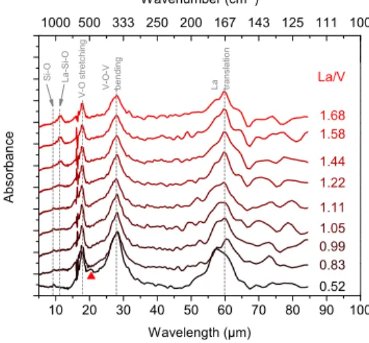
In addition to chemical and structural investigation, a study of infrared properties has been carried out (Figure 9). Three major peaks are visible at 17.9 µm( 559 cm−1), 27.9 µm (358 cm−1) 180
and 59.9 µm (166 cm−1) attributed to the three vibration modes of the perovskite, namely V-O stretching, V-O-V bending and La translation respectively [35]. These vibration modes are not affected by stoichiometry variations. However, the La/V ratio modification leads to the appearance of a peak at 11.13 µm (885 cm−1) attributed to La-O-Si vibration mode [36] and suggests a different structure at the interface with the silicon substrate. A slight contribution at 20.5 µm (487cm−1)
185
appears for La/V ratio of 0.52 and may be attributed to a vanadium oxide. FTIR spectra thus confirm the XPS and XRD analyses with LaVO3-type formation without additional phases for
Lanthanum excess 0.4 0.6 0.8 1.0 1.2 1.4 1.6 1.8 200 210 220 230 240 250 260 270 LaVO 3 + C e l l vo l u m e ( Å 3 )
La/V atomic ratio
Vanadium excess LaVO 3 La 2 O 3
Figure 8: Evolution of the orthorhombic unit cell-volume with the La/V atomic ratio. The red dashed-line distin-guishes the vanadium or lanthanum-richer samples while the blue and green boxes give the structures in presence.
10 20 30 40 50 60 70 80 90 100 1000500 333 250 200 167 143 125 111 100 L a t r a n sl a t io n V -O -V b e n d in g V -O st r e t ch in g L a -S i -O W avenumber (cm -1 ) A b s o r b a n c e W avelength (µm) S i-O 1.05 0.99 0.83 1.22 1.11 1.44 1.58 1.68 0.52 La/V
Figure 9: Absorbance of LaxVyO3 films at different La/V ratios.
XRD diffractograms in Figure 5 reveal the presence of La2O3cubic structure and the XPS
spec-tra shown in Figure 6 reveal the 2p3/2vanadium contribution extinguishment with increasing La/V 190
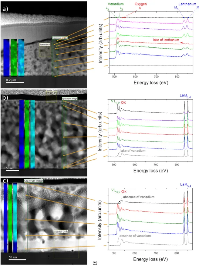
atomic ratio. Those facts are motivating a TEM investigation in order to locate both structures and element positions using respectively fast Fourier transforms of HRTEM images or EELS analyses on three FIB lamellae and both cut using the FIB technique; the first for the V-richer sample with a La/V ratio of 0.52, the second for the La/V = 0.99 sample closest to the stoichiometry and the third for the lanthanum-richer La/V = 1.68 sample.
Several STEM images have been taken with the high angle annular dark field (HAADF) detector in order to select regions for EELS spectrum acquisitions. Figure 10 exhibits the presence of carbon and platinum elements, both used for lamella preparation. Between the lanthanum-vanadium-oxygen film and the silicon substrate, we detect a thin silica film corresponding to native silicon oxide.
200
Figure 10 shows two HAADF cross-section images and for selected regions, the corresponding elemental maps of lanthanum M4,5 edges and vanadium L2,3 edges. Colored intensities depend on
the area of the selected characteristic energy-loss peaks and respectively correspond to lanthanum M4 or vanadium L3 rays among the different EELS spectra acquired for each pixel of the maps.
Then intensities are proportional to the elemental contents. The right color bar representing the
205
total signal of the lanthanum and vanadium EELS peak intensities (in cyan color in the Figure 10.a, 10.b and 10.c) seems to have the same brightness on the whole thickness of the sample with a La/V ratio close to 0.52 (Figure 10.a) meaning that both vanadium and lanthanum are present whatever the depth in the film. Nevertheless, the EELS spectra shown at the right of the figure clearly brings out a region where there is less lanthanum than the others. In the case of the sample with a La/V
210
ratio close to 1 (see Figure 10.b) the right color bar has an almost constant brightness except for the film-substrate border where a lake of vanadium which is confirmed by the lower EELS spectrum at the right of the same figure is observed on a thickness smaller than 3 nm (where the total film thickness is close to 260 nm). However, for the La-rich sample with a ratio near 1.68 and a total film thickness close to 192 nm, the total signal (shown in Figure 10.b) highlights a lake of vanadium
215
close to the film borders, namely up to approximately 6 nm in depth at the surface and 35 nm at the layer-substrate interface, which represents almost 20 percents of the total film thickness could be a potential localization for the formation of La2O3.
In order to study the crystallographic structure, Fast Fourier Transforms (FFT) on HRTEM images or diffraction patterns (not shown) were recorded on different crystallites. As expected, for
220
the La/V = 0.99, only the LaVO3 phase was found. For the lanthanum-deficient sample with the
La/V ratio of 0.52, we have only observed the LaVO3 phase, despite that the regions with less
lanthanum were revealed by EELS for this V-richer sample (see Figure 10.a) and even more, that a signature of vanadium oxides was visible when using on the infrared spectrum (see Figure 9). This fact could be explained by small crystallite sizes of the potential vanadium oxides. On the
225
Figure 10.b) we found La2O3 cubic crystallites (using lattice parameters given in [24]) for almost
three nanometers i.e. approximately the thickness without vanadium found using EELS. At the center of the layer only LaVO3orthorhombic crystallites were identified, surrounded by amorphous
domains. The transition between La2O3and LaVO3regions is not abrupt since a mixture of La2O3 230
and a very few LaVO3orthorhombic crystallites (identified with lattice parameters of [23]) is present
on a thickness of three nanometers despite the low vanadium EELS signal (EELS signal in Figure 10.b). Finally, close to the native silica between the film and the substrate we only detected the presence of the La2O3 cubic structure too. Another surprising fact is the presence of silicon from
the substrate at the interfaces but only for this sample, with a large lanthanum excess which is
235
not occurring before annealing. This fact may be attributed to the possible insertion of the silicon into the La2O3 structure that is confirmed by a La-O-Si infrared vibration mode (Figure 9). The
La2O3/LaVO3 non negligible thickness ratio close to 20 % justifies the La2O3phase present at the
surface and the interface revealed by XRD, XPS and FTIR.
To summarize, the growth window of LaVO3 structure ranges from La/V ratio around 0.5 up 240
to 1.7. The increase of the lanthanum content induces the formation of La2O3 phase containing
silicon at each perovskite film boundaries whereas when increasing the vanadium concentration, vanadium oxides seem to be present in volume, where a lake of lanthanum was observed.
4. Conclusion
The LaVO3growing window has been investigated by the means of LaxVyO3thin films synthesis, 245
by using three complementary characterization methods. The thin films have been elaborated using a two-step method based on the magnetron co-sputtering followed by an ex-situ reducing thermal treatment (under Ar/H2mixture). Surprisingly, the structure presents a high tolerance, even using
an annealing step. FTIR, XPS and XRD analyses clearly demonstrate structural modifications at La/V ratios higher than 1.2 whereas for the La/V ratio of 0.52 the FTIR highlights a new vibration
250
mode, related to the presence of vanadium oxide(s). According to TEM and FTIR observations, vanadium oxide crystallites are present in volume contrary to the La2O3lanthanum oxide observed
at the interface meaning that in the case of a vanadium excess no oxide layer is preferentially formed at the interfaces. This is an interesting fact for photovoltaics applications because stabilizing an unique crystallographic structure means a constant and stable 1.1 eV indirect optical gap in such
255
growth window) could affect the physical properties of a solar cell [37]. Furthermore, the use of magnetron sputtering makes up-scalable process over a large surface possible for example in the solar panels realization.
Acknowledgements
260
The SIAM platform in UNamur (for the XPS measurements) is acknowledged. The authors thank R´egis Peignier from the Institut Jean Lamour of Nancy for his precious technical expertise and J´erˆome Grausem from the LCPME laboratory (Nancy, France) for the FTIR spectrometer used.
This research did not receive any specific grant from funding agencies in the public, commercial,
265
or not-for-profit sectors.
References
[1] E. Manousakis, Photovoltaic effect for narrow-gap Mott insulators, Physical Review B 82 (12) (2010) 125109. doi:10.1103/PhysRevB.82.125109.
URL https://link.aps.org/doi/10.1103/PhysRevB.82.125109
270
[2] T. Arima, Y. Tokura, J. B. Torrance, Variation of optical gaps in perovskite-type 3d transition-metal oxides, Physical Review B 48 (23) (1993) 17006.
URL https://journals.aps.org/prb/abstract/10.1103/PhysRevB.48.17006
[3] W. Shockley, H. J. Queisser, Detailed Balance Limit of Efficiency of p-n Junction Solar Cells, Journal of Applied Physics 32 (3) (1961) 510–519. doi:10.1063/1.1736034.
275
URL http://aip.scitation.org/doi/abs/10.1063/1.1736034
[4] E. Assmann, P. Blaha, R. Laskowski, K. Held, S. Okamoto, G. Sangiovanni, Oxide Het-erostructures for Efficient Solar Cells, Physical Review Letters 110 (7) (2013) 078701. doi: 10.1103/PhysRevLett.110.078701.
URL https://journals-aps-org.bases-doc.univ-lorraine.fr/prl/abstract/10.1103/
280
PhysRevLett.110.078701
[5] H.-T. Zhang, L. R. Dedon, L. W. Martin, R. Engel-Herbert, Self-regulated growth of LaVO3
doi:10.1063/1.4922213.
URL http://aip.scitation.org/doi/abs/10.1063/1.4922213
285
[6] H.-T. Zhang, M. Brahlek, X. Ji, S. Lei, J. Lapano, J. W. Freeland, V. Gopalan, R. Engel-Herbert, High-Quality LaVO3 Films as Solar Energy Conversion Material, ACS Applied
Ma-terials & Interfaces 9 (14) (2017) 12556–12562. doi:10.1021/acsami.6b16007. URL http://dx.doi.org/10.1021/acsami.6b16007
[7] H. Rotella, U. Lders, P.-E. Janolin, V. H. Dao, D. Chateigner, R. Feyerherm, E. Dudzik,
290
W. Prellier, Octahedral tilting in strained LaVO3thin films, Physical Review B 85 (18) (2012)
184101. doi:10.1103/PhysRevB.85.184101.
URL https://link.aps.org/doi/10.1103/PhysRevB.85.184101
[8] W. Choi, T. Sands, K. Kim, Epitaxial growth of semiconducting LaVO3thin films, Journal of
Materials Research 15 (2000) 1–3. doi:10.1557/JMR.2000.0001.
295
URL http://adsabs.harvard.edu/abs/2000JMatR..15....1C
[9] Q. Wang, K. Itaka, H. Minami, H. Kawaji, H. Koinuma, Combinatorial pulsed laser deposition and thermoelectricity of (la1xcax)VO3 composition-spread films, Science and Technology of
Advanced Materials 5 (5) (2004) 543–547. doi:10.1016/j.stam.2004.03.003. URL http://www.sciencedirect.com/science/article/pii/S1468699604000804
300
[10] L. F. Kourkoutis, D. A. Muller, Y. Hotta, H. Y. Hwang, Asymmetric interface profiles in LaVO3SrTiO3 heterostructures grown by pulsed laser deposition, Applied Physics Letters
91 (16) (2007) 163101. doi:10.1063/1.2798060.
URL https://aip.scitation.org/doi/10.1063/1.2798060
[11] W. Sheets, B. Mercey, W. Prellier, Effect of charge modulation in (LaVO3)m(SrVO3)n super-305
lattices on the insulator-metal transition: Applied Physics Letters: Vol 91, No 19, Applied Physics Letters 91 (19). doi:10.1063/1.2805222.
URL https://aip.scitation.org/doi/abs/10.1063/1.2805222?journalCode=apl
[12] M. Jellite, J. L. Rehspringer, M. A. Fazio, D. Muller, G. Schmerber, G. Ferblantier, S. Colis, A. Dinia, M. Sugiyama, A. Slaoui, D. Cavalcoli, T. Fix, Investigation of LaVO3 based com-310
2017.12.061.
URL https://www.sciencedirect.com/science/article/pii/S0038092X1731143X
[13] D. Mercs, A. Didelot, F. Capon, J.-F. Pierson, B. Hafner, A. Pazidis, S. Fste, R. Reineke-Koch, Innovative Smart Selective Coating to Avoid Overheating in Highly Efficient Thermal Solar
315
Collectors, Energy Procedia 91 (2016) 84–93. doi:10.1016/j.egypro.2016.06.177. URL http://www.sciencedirect.com/science/article/pii/S1876610216302752
[14] E. Haye, V. Pierron, S. Barrat, F. Capon, F. Munnik, S. Bruy`ere, Nitrogen redistribution in annealed LaFeOxNythin films investigated by FTIR spectroscopy and EELS mapping, Applied
Surface Science 427 (2018) 1041–1045. doi:10.1016/j.apsusc.2017.09.090.
320
URL http://www.sciencedirect.com/science/article/pii/S0169433217327393
[15] E. Haye, S. Bruyere, E. Andr´e, P. Boulet, S. Barrat, F. Capon, P. Miska, S. Migot, C. Carteret, R. Coustel, C. Gendarme, S. Diliberto, F. Munnik, LaFeOxNy perovskite thin films: Nitrogen
location and its effect on morphological, optical and structural properties, Journal of Alloys and Compounds 724 (2017) 74 – 83. doi:10.1016/j.jallcom.2017.07.025.
325
URL https://hal.univ-lorraine.fr/hal-01767763
[16] E. Haye, F. Capon, S. Barrat, D. Mangin, J.-F. Pierson, Phenomenological study of iron and lanthanum magnetron co-sputtering using two reactive gases, Surface and Coatings Technology 298. doi:10.1016/j.surfcoat.2016.04.039.
[17] E. Haye, F. Capon, S. Barrat, P. Boulet, E. Andre, C. Carteret, S. Bruyere, Properties of
rare-330
earth orthoferrites perovskite driven by steric hindrance, Journal of Alloys and Compounds 657 (2016) 631–638. doi:10.1016/j.jallcom.2015.10.135.
URL http://www.sciencedirect.com/science/article/pii/S0925838815313918
[18] F. Capon, A. Boileau, C. Carteret, N. Martin, P. Boulet, J. F. Pierson, Cation size effect on the thermochromic properties of rare earth cobaltites RECoO3 (RE: La, Nd, Sm), Journal of 335
Applied Physics 114 (11) (2013) 113510. doi:10.1063/1.4821884.
URL https://aip-scitation-org.bases-doc.univ-lorraine.fr/doi/full/10.1063/1. 4821884
[19] M. F. Sunding, K. Hadidi, S. Diplas, O. M. Lvvik, T. E. Norby, A. E. Gunns, XPS charac-terisation of in situ treated lanthanum oxide and hydroxide using tailored charge referencing
and peak fitting procedures, Journal of Electron Spectroscopy and Related Phenomena 184 (7) (2011) 399–409. doi:10.1016/j.elspec.2011.04.002.
URL http://www.sciencedirect.com/science/article/pii/S0368204811000727
[20] F. Capon, D. Horwat, J. F. Pierson, V. Chapusot, A. Billard, Strontium-doped lanthanum manganite coatings crystallised after air annealing of amorphous co-sputtered films, Materials
345
Chemistry and Physics 116 (1) (2009) 219–222. doi:10.1016/j.matchemphys.2009.03.021. URL http://www.sciencedirect.com/science/article/pii/S0254058409001631
[21] D. Depla, G. Buyle, J. Haemers, R. De Gryse, Discharge voltage measurements during magnetron sputtering, Surface and Coatings Technology 200 (14) (2006) 4329–4338. doi: 10.1016/j.surfcoat.2005.02.166.
350
URL http://www.sciencedirect.com/science/article/pii/S0257897205003634
[22] A. Boileau, F. Capon, P. Laffez, S. Barrat, J. L. Endrino, R. E. Galindo, D. Horwat, J. F. Pierson, Mechanisms of Oxidation of NdNiO3−δ Thermochromic Thin Films Synthesized by a
Two-Step Method in Soft Conditions, The Journal of Physical Chemistry C 118 (11) (2014) 5908–5917. doi:10.1021/jp4111597.
355
URL https://doi.org/10.1021/jp4111597
[23] H. Seim, H. Fjellvg, B. C. Hauback, A. Gumm, S. Larsen, Non-Stoichiometric LaVO3. II.
Powder Neutron Diffraction Study of Crystal and Magnetic Structure for La1− xVO3, 0.00
<= X <= 0.10., Acta Chemica Scandinavica 52 (1998) 1301–1306. doi:10.3891/acta.chem. scand.52-1301.
360
URL http://actachemscand.org/doi/10.3891/acta.chem.scand.52-1301
[24] A.-E. Gobichon, J.-P. Auffrdic, D. Lour, Potassium Lanthanum Nitrate System: Phase Equi-libria and Thermal and Structural Properties, Journal of Solid State Chemistry 144 (1) (1999) 68–80. doi:10.1006/jssc.1998.8119.
URL http://www.sciencedirect.com/science/article/pii/S0022459698981191
365
[25] M. C. Biesinger, L. W. M. Lau, A. R. Gerson, R. S. C. Smart, Resolving surface chemical states in XPS analysis of first row transition metals, oxides and hydroxides: Sc, Ti, V, Cu and Zn, Applied Surface Science 257 (2010) 887–898. doi:10.1016/j.apsusc.2010.07.086. URL http://adsabs.harvard.edu/abs/2010ApSS..257..887B
[26] Y. Hotta, H. Wadati, A. Fujimori, T. Susaki, H. Y. Hwang, Electronic structure of the Mott
370
insulator LaVO3in a quantum well geometry, Applied Physics Letters 89 (25) (2006) 251916.
doi:10.1063/1.2422898.
URL http://aip.scitation.org/doi/abs/10.1063/1.2422898
[27] L. Wang, Y. Li, A. Bera, C. Ma, F. Jin, K. Yuan, W. Yin, A. David, W. Chen, W. Wu, W. Prellier, S. Wei, T. Wu, Device Performance of the Mott Insulator LaVO3as a Photovoltaic 375
Material, Physical Review Applied 3 (6). doi:10.1103/PhysRevApplied.3.064015. URL https://link.aps.org/doi/10.1103/PhysRevApplied.3.064015
[28] A. Jana, R. J. Choudhary, D. M. Phase, Mott-Hubbard type insulating nature of epitaxial LaV O 3 thin films, Physical Review B 98 (7) (2018) 075124. doi:10.1103/PhysRevB.98.075124. URL https://link.aps.org/doi/10.1103/PhysRevB.98.075124
380
[29] H. Wadati, Y. Hotta, M. Takizawa, A. Fujimori, T. Susaki, H. Y. Hwang, Characterization of LaVOx thin films by photoemission spectroscopy, Journal of Applied Physics 102 (5) (2007) 053707. doi:10.1063/1.2775889.
URL http://aip.scitation.org/doi/10.1063/1.2775889
[30] R. Scurtu, G. Nechifor, C. Andronescu, V. Fruth, P. Osiceanu, La0.8Sr0.2Ga0.83Mg0.17O3−δ 385
perovkites investigated by impedance spectroscopy and X-ray photoelectron spectroscopy, U.P.B. Sci. Bull., Series B 76 (2014) 67–76.
[31] K. Bolwin, W. Schnurnberger, G. Schiller, Influence of valence band states on the core hole screening in lanthanide perovskite compounds, Zeitschrift fr Physik B Condensed Matter 72 (2) (1988) 203–209. doi:10.1007/BF01312136.
390
URL https://link.springer.com/article/10.1007/BF01312136
[32] S. Mickeviius, S. Grebinskij, V. Bondarenka, B. Vengalis, K. liuien, B. A. Orlowski, V. Osinniy, W. Drube, Investigation of epitaxial LaNiO3−xthin films by high-energy XPS, Journal of Alloys
and Compounds 423 (1) (2006) 107–111. doi:10.1016/j.jallcom.2005.12.038. URL http://www.sciencedirect.com/science/article/pii/S0925838805019171
395
[33] S. Han, J. Lee, K. H. Kim, H. Song, W. Kim, S. Kwon, H.-G. Lee, C. Hwang, J. Jeong, J.-S. Kang, Electronic structures of the CMR perovskites R1−xAxMnO3 (R = La, Pr; A = Ca,
Sr, Ce) using photoelectron spectroscopy, Journal of the Korean Physical Society 40 (2002) 501–510.
[34] P. Bordet, C. Chaillout, M. Marezio, Q. Huang, A. Santoro, S.-W. Cheong, H. Takagi,
400
C. Oglesby, B. Batlogg, Structural Aspects of the Crystallographic-Magnetic Transition in LaVO3 around 140 K, Journal of Solid State Chemistry 106 (2) (1993) 253–270. doi:
10.1006/jssc.1993.1285.
URL http://www.sciencedirect.com/science/article/pii/S0022459683712855
[35] E. Haye, E. Andre, F. Capon, S. Barrat, M. De La Pierre, R. Dovesi, C. Carteret, Experimental
405
and Theoretical Infrared Signatures of REMO3 (RE = La, Pr, Nd, Sm, and M = Co, Fe)
Perovskites, The Journal of Physical Chemistry C 122 (19) (2018) 10519–10525. doi:10. 1021/acs.jpcc.8b01433.
URL https://doi.org/10.1021/acs.jpcc.8b01433
[36] J. Kwon, M. Dai, M. D. Halls, E. Langereis, Y. J. Chabal, R. G. Gordon, In Situ Infrared
410
Characterization during Atomic Layer Deposition of Lanthanum Oxide, The Journal of Phys-ical Chemistry C 113 (2) (2009) 654–660. doi:10.1021/jp806027m.
URL https://doi.org/10.1021/jp806027m
[37] S. F. Shaikh, H.-C. Kwon, W. Yang, H. Hwang, H. Lee, E. Lee, S. Ma, J. Moon, La2O3
inter-face modification of mesoporous TiO2 nanostructures enabling highly efficient perovskite solar 415
cells, Journal of Materials Chemistry A 4 (40) (2016) 15478–15485. doi:10.1039/C6TA05008E. URL https://pubs-rsc-org.bases-doc.univ-lorraine.fr/en/content/ articlelanding/2016/ta/c6ta05008e
Figure 10: HAADF images of the (a) La/V = 0.52, (b) La/V = 0.99 and (c) La/V = 1.68 sample cross-sections. For the selected area an EELS spectrum was taken each 2 nanometers and elemental maps of both lanthanum and