HAL Id: hal-03187841
https://hal.archives-ouvertes.fr/hal-03187841
Submitted on 1 Apr 2021HAL is a multi-disciplinary open access archive for the deposit and dissemination of sci-entific research documents, whether they are pub-lished or not. The documents may come from teaching and research institutions in France or abroad, or from public or private research centers.
L’archive ouverte pluridisciplinaire HAL, est destinée au dépôt et à la diffusion de documents scientifiques de niveau recherche, publiés ou non, émanant des établissements d’enseignement et de recherche français ou étrangers, des laboratoires publics ou privés.
Effect of Temperature on Single Event Latchup
Sensitivity
S. Guagliardo, Frédéric Wrobel, Ygor Quadros de Aguiar, Jean-Luc Autran, P.
Leroux, Frédéric Saigné, Vincent Pouget, Antoine Touboul
To cite this version:
S. Guagliardo, Frédéric Wrobel, Ygor Quadros de Aguiar, Jean-Luc Autran, P. Leroux, et al.. Effect of Temperature on Single Event Latchup Sensitivity. International Conference on Design and Technology of Integrated Systems in Nanoscale Era (DTIS), Apr 2020, Marrakech, Morocco. �10.1109/dtis48698.2020.9081275�. �hal-03187841�
1
Abstract - Single-Event Latchup (SEL) concerns CMOS technology as a major reliability issue and it is influenced by different parameters. In this work, the effect of the temperature variation on SELhas been investigated and its effect has been analyzed combining the variation of three parameters related to the geometry and to the design of the component: doping profile, anode to cathode spacing (A-C spacing) and substrate and well taps placement. 2D TCAD simulations have been performed, using an NPNP structure based on 65nm CMOS inverter. From these simulations, we have analyzed threshold LET and SEL rate. Results show that temperature impact is stronger when the component is less sensitive to SEL.
Index Terms – Single-Event Latchup, TCAD simulations, Cross section.
I. INTRODUCTION
INGLE-Event Latchup (SEL) is a serious reliability concern for CMOS devices. It arises from parasitic bipolar transistors that are structurally intrinsic to this technology (Fig. 1) [1]–[4]. Temperature is one of the most important parameters that influences SEL sensitivity. Literature results showed that as an impact on Single-Event Latchup cross section, which is dependent on the range of temperature considered [5]–[7]. Nonetheless, SEL sensitivity is influenced by a combination of numerous factors. In fact, component design must be considered to determine the probability of Single-Event Latchup in a device. Different studies have been performed in which other factors are considered. For instance, doping profile, substrate and well taps placement and anode to cathode spacing have been investigated in the literature, revealing that SEL sensitivity depends on them [8]–[16]. However, it is also interesting to analyze the behavior of cross section when these factors are combined. In our work, TCAD simulations have been performed to assess their impact. Firstly, we have analyzed the effect of the variation of the design parameters (doping profile, substrate and well taps placement and anode to cathode spacing) on SEL sensitivity. Then, we
Manuscript received January 31, 2020. This work was realized within RADSAGA project. The RADSAGA Innovative Training Network project has received funding from the European Union’s Horizon 2020 research and innovation program under the Marie-Skłodowska-Curie grant agreement number 721624.
S. Guagliardo, F. Wrobel, Y. Q. Aguiar, F. Saigné, A. D. Touboul and V. Pouget are with Université de Montpellier, IES-UMR UM/CNRS 5214, 860
have investigated, considering a specific range of temperatures, how temperature affects the effect of each parameter. In order to achieve our goal, we have calculated SEL cross sections, following a 2D approach. As a result, more detailed information on the device SEL sensitivity are available. Beside the cross-section curves, it was also estimated the in-orbit SEL rate for GEO.
The structure of the paper is the following: in Section II we explain the methodology used and in Section III how we performed TCAD simulations and how we calculated SEL cross section curves. In Section IV results are presented and discussed, and finally Section V includes our conclusions.
II. METHODOLOGY
As aforementioned, we have taken into consideration three parameters: doping profile of the whole structure, well and substrate taps placement and anode to cathode spacing (A-C spacing). Each parameter has been evaluated for a set of values and for a range of temperatures. Then, cross section has been calculated for every case. In order to achieve our goal, we have performed 2D TCAD simulations. Despite the three-dimensional nature of the SEL mechanism, we decided to perform 2D simulations. In fact, it has been demonstrated that 3D simulations follow the same trend as in 2D simulations [9], [17].
Rue Saint-Priest, Bat. 5, F-34097, Montpellier, France (corresponding author email: [email protected]).
J-L. Autran is with the Institut Materiaux Microelectronique Nanoscience de Provence, Aix-Marseille Université, Marseille, France.
P. Leroux is with Advanced Integrated Sensing Lab, KU Leuven University, Leuven, Belgium.
Effect of the Temperature on Single Event
Latchup Sensitivity
S. Guagliardo, F. Wrobel, Y.Q. Aguiar, J-L. Autran, P. Leroux, F. Saigné, V. Pouget and A.D. Touboul
S
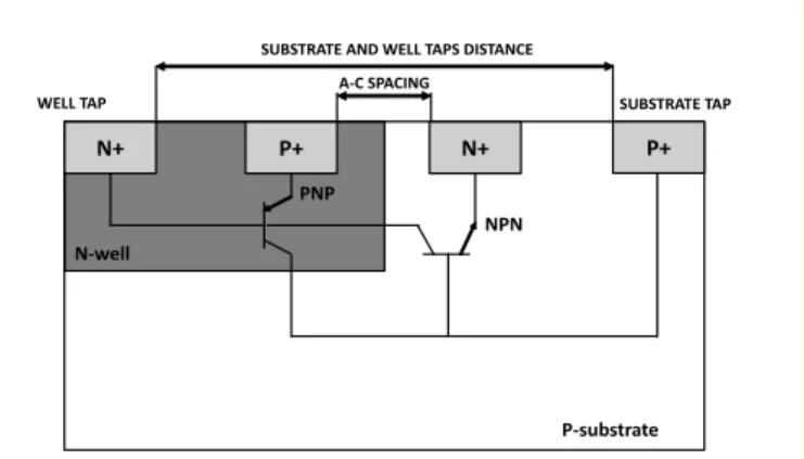
Fig. 1. Simplified NPNP structure used in our work. A-C spacing is depicted.
N+ P+ N+ P+
PNP
NPN
A-C SPACING SUBSTRATE AND WELL TAPS DISTANCE
WELL TAP SUBSTRATE TAP
N-well
P-substrate
Cite this article as: S. Guagliardo et al., "Effect of the Temperature on Single Event Latchup Sensitivity," 2020 15th Design & Technology of Integrated Systems in Nanoscale Era (DTIS), Marrakech, Morocco, 2020, pp. 1-5, doi: 10.1109/DTIS48698.2020.9081275.
2 Thus, considering that we are interested in the trend of cross
section, we have chosen to perform 2D simulations using Sentaurus Synopsys tool. TCAD simulations have been extensively used in the literature and thanks to them, it is possible to investigate mechanism of SEL by providing an insight view of the device. Due to the well-developed physical models available in TCAD tools, it is also possible to retrieve data that are useful to calculate parameters that are strictly related to radiation sensitivity, like cross section.
Here, we focused our analysis on the effects of temperature for A-C spacing, doping profiles variation and substrate and well taps placement. The aim is to verify to what extent SEL dependence on each parameter is highly influenced by the temperature variation. Additionally, we have calculated cross-section curves from 2D simulations and from them we have estimated SEL rate. In this way, we have analyzed the sensitivity of the device for the whole linear energy transfer (LET) range and not only in term of threshold LET. Hence, when specific parameters are selected for a design, these results can indicate if temperature variation will strongly modify the behavior of SEL sensitivity.
III. TCADSIMULATIONS
A. Device structure and simulation setup
The first step was to design a CMOS inverter using design data for a commercially available bulk 65nm technology with Cadence Virtuoso. Based on the physical layout of the minimum-sized inverter, an NPNP structure (Fig. 1) has been retrieved. This structure is formed by the PMOS and the NMOS source and it is the basic structure required to investigate SEL mechanisms [1]. Firstly, we have chosen the range of temperature to use for simulations. Temperatures of 350 K, 375 K, 400 K and 425 K have been chosen. As we know, SEL is more likely at higher temperature, so we have chosen a set of temperature in which it was more likely to obtain Single-Event Latchup. Secondly, we have chosen five values for each parameter to explore a broad range of possibilities. Thus, for
substrate and well taps placement we considered their distance and we have chosen 1.05, 1.25, 1.55, 1.85 and 2.15 µm, moving taps symmetrically further from the center. Doping profile of the whole structure has been modified by multiplying a reference value, based on a commercial bulk 65nm process, times 0.75, 0.85, 1.15 and 1.25. Its value was changed across the whole structure. Eventually, these five values have been chosen for A-C spacing: 0.25, 0.27, 0.32, 0.37 and 0.40 µm.
In order to perform simulations on Sentaurus Synopsys we needed to choose physical models. We have chosen proper models for a 65 nm technology and they have been based on previous literature [7], [18], [19]. The hydrodynamic model has been chosen along with Fermi statistics as carrier transport model. The mobility was modelled with the built-in model by Arora [20], which is a doping and temperature dependent model. For recombination the doping dependent Shockley-Read-Hall, Auger recombination and avalanche generation have been chosen. Finally, bandgap narrowing for high doped region has been selected.
Ion track has been generated through the built-in tool on Sentaurus Synopsys. A range of 2.3 µm in order to cover the entire structure with a constant linear energy transfer has been selected. The radial distribution has been set with a Gaussian profile with a 50 nm radius, according to previous works [10], [19].
B. Cross section calculation
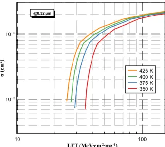
In order to calculate cross section, we followed the approach as reported in [21]. At first, threshold LET was obtained for different positions along the device and a chart was created, as the one in Fig. 2. From this chart, it is then possible to calculate for every LETx value, which portion (that we call “sensitive zone”) of the device is sensitive to Single-Event Latchup for that value of LET. By multiplying the sensitive zone by the width of the component, the cross section is calculated. The width is in the order of magnitude of µm. An example of cross section curve is shown in Fig. 3.
Fig. 3. Example of cross section curve calculated by 2D approach. It shows the variation of cross section (σ) for different temperatures.
Fig. 2. Minimum LET value versus position along the component.
3
IV. RESULTS AND DISCUSSION
A. Threshold LET
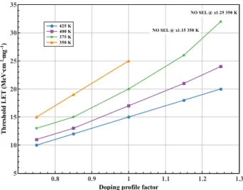
First, in Fig. 4, the threshold LET trend for doping profiles is shown. More specifically, it is shown the trend for the range of temperature considered. As expected, threshold LET decreases as the temperature increases and increases as the doping profile increases [8]. Moreover, it is interesting to focus on the trend. If we consider the condition in which the device design is more favorable to induce Single-Event Latchup, as the worst-case scenario (lowest threshold LET, i.e. lower doping level) and the best-case scenario as the opposite, we can observe that the threshold LET difference for each single doping case, increases as the conditions become less favorable to SEL. In fact, in the worst-case scenario, the difference between threshold LET at 425 K and at 350 K is 50%, meanwhile in the best-case scenario a difference of 60% is reached between 425 K and 375 K. Moreover, at 350 K, no SEL is observed for x1.15 and x1.25 case, which are thus the best condition for immunity.
In Fig. 5, threshold LET curve for substrate and well taps placement are shown. Thresholds decrease as the temperature decreases and it is higher as taps are placed closer to the center of the device, which is confirmed by literature. Furthermore, temperature influence can be also seen in this case. In the worst-case scenario, the difference between 350 K and 425 K is 50% and as we have seen previously, in the best-case scenario the difference becomes higher. Indeed, threshold LET is increased by 75% just between 425 K and 375 K and at 350 K SEL is not even achieved.
Eventually, in Fig. 6 threshold LET curves for anode to cathode spacing are shown. The trend that has been observed for the previous parameters is also confirmed for the A-C spacing. Regarding this condition, in the worst case, threshold LET between the lower and the higher temperature increases by 58%, meanwhile in the best-case scenario threshold increases by 53% between 425 K and 375 K and SEL is not reached for 350 K. In this case, the difference is smaller with respect to previous examples. The reason may be that the effects of anode
to cathode spacing variation is lower with respect to the other parameters.
In conclusion, for all the conditions investigated, temperature influence on SEL sensitivity is lower when conditions are more favorable to SEL and increases as parameters are modified to make the component less sensitive.
B. SEL rate
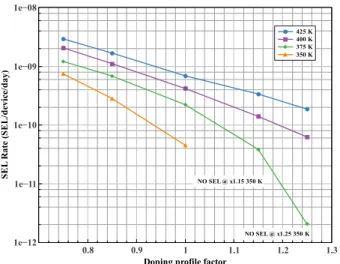
To further investigate this trend, we have calculated the SEL rate for a specific orbit, using OMERE, a free software dedicated to space environments [22]. Cross sections calculated with the 2D approach (Fig. 3) have been used to calculate the SEL rate. Regarding the doping profile, in Fig. 7, it can be seen that SEL rate follow the same trend observed for threshold LET. Considering that SEL rate takes into consideration the whole cross section, it means that the trend that has been seen for the threshold LET is present even for higher LET. Considering, 425 K as a reference, SEL rate increases from 30% to 40% for the worst case (x0.75), it increases from 40% to 80% when reference doping profile is analyzed, and increases from 70% to
Fig. 4. Threshold LET vs doping profile for four different temperatures (350 K, 375 K, 400 K and 425 K).
Fig. 5. Threshold LET vs substrate and well taps distance for four different temperatures (350 K, 375 K, 400 K and 425 K).
Fig. 6. Threshold LET vs anode to cathode spacing for four different temperatures (350 K, 375 K, 400 K and 425 K).
4
97% for the best-case scenario (x1.25, which is not calculated at 350 K because SEL was not obtained). In Fig. 8, it is shown the SEL rate for substrate and well taps placement. Even in this case, the trend is confirmed. SEL rate increases from 35% to 40% for the best-case scenario and it increases from 65% to 88% in the worst-case scenario. Eventually, SEL rate for A-C spacing is presented (Fig. 9). SEL rate varies from 46% to 82% for the best case and from 37% to 54% in the worst case.
C. Discussion
From the results it can be observed that temperature plays a different role depending on the condition of the device. When conditions of the device are favorable to SEL, temperature variation is affecting threshold LET and SEL rate less relevantly than in the case if which the device is more hardened. In order to explain that, SEL triggering conditions must be considered. As aforementioned, the structure of the CMOS creates two parasitic transistors inside it. The activation of these transistors is the initial step for Single-Event Latchup. Hence, a circuit is created inside the structure as depicted by [1]. Certainly, the characteristic of the circuit is related to the design of the device and then, a variation of a parameter leads to a variation of the response of the circuit and then to a variation on SEL sensitivity. Specifically, the doping profile influences the PNP bipolar current gain and the resistances inside the device [8]. Substrate and well taps placement variation causes a modification of the resistances present inside the device. A lower resistance will reduce SEL sensitivity, meanwhile a higher resistance will increase it. Concerning the A-C spacing, if it is increased, the bipolar current gain is decreased (as similarly observed for the doping profile). Eventually, temperature modification will cause a change on the resistances and it will modify the forward bias voltage of the base-emitter junction. A variation of this parameter means a variation of the potential barrier needed to trigger SEL [19].
However, SEL sensitivity is clearly dependent to a combination of all these effects. This work shows that for all the parameters (doping profile, substrate and well taps placement and A-C spacing) a more relevant variation of threshold LET and SEL rate is obtained for the best-case
scenario, with respect to the worst-case scenario. On first consideration, we can say that in the best-case scenario, conditions are already favorable to SEL immunity and then the decrease of temperature will help to increase SEL immunity of the device. Meanwhile, in the worst-case scenario, the device situation is already on SEL favor. Then, temperature will have a lower effect on SEL sensitivity. In general, it can be considered that temperature impact is not equal in all conditions and it is not independent from device design.
V. CONCLUSION
In this work a comparison between the effect of temperature on four different parameters has been made. Cross-section curves for each parameter have been calculated using 2D TCAD simulations and then SEL rate has been estimated from these curves. For each parameter, we have modified its value and then for each single case we have investigate temperature effects, for a chosen temperature range. At first, threshold LET is investigated. We have observed, for every case, that when the component is less sensitive to SEL, temperature has a stronger impact on threshold LET, with respect to the opposite case. To further investigate this trend, we have calculated SEL rate for
Fig. 7. SEL rate vs doping profile for four different temperatures (350 K, 375 K, 400 K and 425 K).
Fig. 8. SEL rate vs substrate and well taps distance for four different temperatures (350 K, 375 K, 400 K and 425 K).
Fig. 9. SEL rate vs anode to cathode spacing for four different temperatures (350 K, 375 K, 400 K and 425 K).
5 the GEO orbit. Indeed, the same trend has been observed for
SEL rate. In the extended version of the paper, we will investigate this aspect.
ACKNOWLEDGEMENT
This work was realized within RADSAGA project. The RADSAGA Innovative Training Network project has received funding from the European Union’s Horizon 2020 research and innovation program under the Marie-Skłodowska-Curie grant agreement number 721624.
REFERENCES
[1] G. Bruguier and J.-M. Palau, ‘Single Particle Induced
Latchup.pdf’, IEEE Transactions on Nuclear Science, vol. 43, no. 2, pp. 522–532, Apr-1996.
[2] T. Aoki, ‘Dynamics of heavy-ion induced latchup in CMOS
structures’, IEEE Transactions on Electron Devices, vol. 35, no. 11, pp. 1885–1891, Nov-1998.
[3] M. Shoga and D. Binder, ‘Theory of Single Event Latchup in
Complementary Metal-Oxide Semiconductor Integrated
Circuits’, IEEE Transactions on Nuclear Science, vol. 33, no. 6, pp. 1714–1717, 1986, doi: 10.1109/TNS.1986.4334671.
[4] A. H. Johnston, ‘Mechanisms for single-particle latchup in
CMOS structures’, in RADECS 93. Second European
Conference on Radiation and its Effects on Components and Systems (Cat. No.93TH0616-3), St. Malo, France, 1994, pp.
433–437, doi: 10.1109/RADECS.1993.316564.
[5] A. H. Johnston, B. W. Hughlock, M. P. Baze, and R. E. Plaag,
‘The effect of temperature on single-particle latchup’, IEEE
Transactions on Nuclear Science, vol. 38, no. 6, pp. 1435–
1441, Dec. 1991, doi: 10.1109/23.124129.
[6] H. Iwata and T. Ohzone, ‘Numerical simulation of single event
latchup in the temperature range of 77-450 K’, IEEE
Transactions on Nuclear Science, vol. 42, no. 3, pp. 148–154,
Jun. 1995, doi: 10.1109/23.387354.
[7] A. A. Youssef, L. Artola, S. Ducret, G. Hubert, and F. Perrier,
‘Analysis of low temperature on single event Latchup mechanisms by TCAD simulations for applications down to 50K’, in 2016 16th European Conference on Radiation and Its
Effects on Components and Systems (RADECS), Bremen, 2016,
pp. 1–5, doi: 10.1109/RADECS.2016.8093175.
[8] N. Rezzak and J.-J. Wang, ‘Single Event Latch-Up Hardening
Using TCAD Simulations in 130nm and 65nm Embedded SRAM in Flash-Based FPGAs’, IEEE Transactions on Nuclear
Science, vol. 62, no. 4, pp. 1599–1608, Aug. 2015, doi:
10.1109/TNS.2015.2450210.
[9] J. M. Hutson, R. D. Schrimpf, and L. M. Massengill, ‘The
Effects of Scaling and Well and Substrate Contact Placement on Single Event Latchup in Bulk CMOS Technology’, in 2005
8th European Conference on Radiation and Its Effects on Components and Systems, Cap d’Agde, France, 2005, pp.
PC24-1-PC24-5, doi: 10.1109/RADECS.2005.4365577. [10] A. A. Youssef, ‘Etude par modélisation des évènements
singuliers (SET/SEU/SEL) induits par l’environnement radiatif dans les composants électroniques’, Institut Superior de l'Aeronatique et de l'Espace (ISAE), 2017.
[11] H. de La Rochette, G. Bruguier, J. M. Palau, J. Gasiot, and R. Ecoffet, ‘The effect of layout modification on latchup triggering in CMOS by experimental and simulation approaches’, IEEE
Transactions on Nuclear Science, vol. 41, no. 6, pp. 2222–
2228, Dec. 1994, doi: 10.1109/23.340566.
[12] J. M. Hutson et al., ‘Evidence for Lateral Angle Effect on Single-Event Latchup in 65 nm SRAMs’, IEEE Transactions
on Nuclear Science, vol. 56, no. 1, pp. 208–213, Feb. 2009, doi:
10.1109/TNS.2008.2010395.
[13] J. M. Hutson, ‘Single Event Latchup in a deep submicron CMOS technology', Ph.D thesis, Vanderbilt Univ., Nashville, TN, USA, Dec. 2008.
[14] A. A. Youssef, L. Artola, S. Ducret, G. Hubert, and F. Perrier, ‘Investigation of Electrical Latchup and SEL Mechanisms at Low Temperature for Applications down to 50K’, IEEE
Transactions on Nuclear Science, pp. 1–1, 2017, doi:
10.1109/TNS.2017.2726684.
[15] A. H. Johnston, ‘The influence of VLSI technology evolution on radiation-induced latchup in space systems’, IEEE
Transactions on Nuclear Science, vol. 43, no. 2, pp. 505–521,
Apr. 1996, doi: 10.1109/23.490897.
[16] N. A. Dodds, N. C. Hooten, R. A. Reed, R. D. Schrimpf, J. H. Warner, N. J.-H. Roche, D. McMorrow, S. Buchner, S. Jordan, J. A. Pellish, W. G. Bennett, N. J. Gaspard, and M. P. King, ‘SEL-Sensitive Area Mapping and the Effects of Reflection and Diffraction from Metal Lines on Laser SEE Testing’, IEEE
Transactions on Nuclear Science, vol. 60, no. 4, pp. 2550–
2558, Aug. 2013, doi: 10.1109/TNS.2013.2246189.
[17] Y. Moreau; H. de la Rochette; G. Bruguier; J. Gasiot; F. Pelanchon; C. Sudre; R. Ecoffet, ‘The latchup risk of CMOS-technology in space’, IEEE Transactions on Nuclear Science, vol. 40, no. 6, pp. 1831–1837, Dec. 1993, doi: 10.1109/23.273473.
[18] Y. Gawlina, L. Borucki, G. Georgakos, and G. Wachutka, ‘Transient 3D Simulation of Single Event Latchup in Deep Submicron CMOS-SRAMs’, in 2009 International Conference
on Simulation of Semiconductor Processes and Devices, San
Diego, CA, USA, 2009, pp. 1–4, doi:
10.1109/SISPAD.2009.5290213.
[19] L. Artola, G. Hubert, and T. Rousselin, ‘Single-Event Latchup Modeling Based on Coupled Physical and Electrical Transient Simulations in CMOS Technology’, IEEE Transactions on
Nuclear Science, vol. 61, no. 6, pp. 3543–3549, Dec. 2014, doi:
10.1109/TNS.2014.2362857.
[20] N. D. Arora, J. R. Hauser, and D. J. Roulston, ‘Electron and hole mobilities in silicon as a function of concentration and temperature’, IEEE Transaction on Electron Devices, vol. 29, no. 2, pp. 292–295, Feb. 1982, doi: 10.1109/T-ED.1982.20698. [21] H. de La Rochette, G. Bruguier, J.-M. Palau, J. Gasiot, and R. Ecoffet, ‘Simulation of heavy ion latchup cross section curves’, in Proceedings of the Third European Conference on Radiation
and its Effects on Components and Systems, Arcachon, France,
1996, pp. 359–364, doi: 10.1109/RADECS.1995.509803. [22] A. Varotsou, ‘OMERE 5.0, 2017, [online]’. [Online].