HAL Id: hal-01793783
https://hal.archives-ouvertes.fr/hal-01793783
Submitted on 16 May 2018HAL is a multi-disciplinary open access archive for the deposit and dissemination of sci-entific research documents, whether they are pub-lished or not. The documents may come from teaching and research institutions in France or abroad, or from public or private research centers.
L’archive ouverte pluridisciplinaire HAL, est destinée au dépôt et à la diffusion de documents scientifiques de niveau recherche, publiés ou non, émanant des établissements d’enseignement et de recherche français ou étrangers, des laboratoires publics ou privés.
First investigations on the feasibility of integration of a
smart sensor in harsh environment 1
S. Ben Krit, W. Rahajandraibe, K. Coulie-Castellani, G. Micolau
To cite this version:
S. Ben Krit, W. Rahajandraibe, K. Coulie-Castellani, G. Micolau. First investigations on the feasibility of integration of a smart sensor in harsh environment 1. International Conference on Advancements in Nuclear Instrumentation, Measurements Methods and their Applications (ANIMMA 2013), Jun 2013, Marseille, France. �hal-01793783�
First investigations on the feasibility of
integration of a smart sensor in harsh
environment
1
S. Ben-Krit,
1W. Rahajandraibe,
1K.
Coulié-Castellani,
2G. Micolau
1IM2NP-UMR CNRS 7334 / Aix-Marseille University
IM2NP, IMT Technopôle de Château – Gombert, 13451 Marseille Cedex 20, France
2UMR 1114 EMMAH (INRA-UAPV)
This very first study takes place in the framework of the I_SMART European project. The final system will consist of one or more detectors in silicon carbide (spectroscopic detector, neutron, gamma …), a readout electronic, a conditioning chain and microprocessor for the signal recognition. The work presented here is dedicated to a first approach of the feasibility of integration of the full system. This system will have to to work in harsh environment in terms of temperature and radiations what makes necessary the development of specifications for operation and reliability of the components and the investigation of margins for the interplay of the components.
When an incident particle, emitted by a source of radiation tracks a semi-conductor (p-n junction for example), direct generated ions or secondary products from proton or neutron/nucleus interactions generate electron-holes pairs [1]. Then, electrons drift within the semi-conductor and diffuse towards a collecting anode inducing a parasitic current. Such kind of behavior is called single effect which differs from cumulative effects (dose effects) that are linked to the presence of oxide in the component [2]. Thus, radiation sensors require pulse processing electronics so that energy or time information involved with radiation interactions (parasitic currents) can be properly extracted.
Several types of detectors can be found in literature. Depending on the needs, they can be divided on two broad categories. A lot of detectors are based on SRAM detection which is only able to ensure information about the number of incident particles detected by the sensor. Other detectors are based on collection and amplification by the use of the silicon sensor (p-n junction) as volume in order to provide information about the generated currents characteristics. Generally, the collection is assured by a matrix of pixels to ensure high
sensitivity [1]. Although this second type requires a whole analog preprocessing chain comprising several components, it is still the more required one due to the importance of information that can be provided on its outputs. The readout chain is mainly composed by i) blocks ensuring amplification, based on a charge sensitive amplifier (CSA) or a current sensitive amplifier (ISA), ii) pulse-shaping that is assured by a pulse shaping amplifier (PSA) providing a semi-Gaussian pulse and iii) an analog to digital conversion (ADC) which provides a digital data ready to pass on to iv) digital signal processing (DSP) [3] [4].
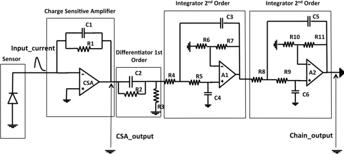
Since the readout electronics has to be placed as close as possible to the sensor to ensure high sensitivity, the full system must be able to work under several constraints (very high temperature and irradiations). However, providing electronic components able to run normally under a temperature higher than 400° and under radiative environment is still a real challenge in the area of the electronic instrumentation. In this context, this first work aims to provide first investigations on the feasibility of integration of the full system in these conditions. It focuses essentially on the development of the specifications for operation (signal to noise ratio (SNR), bandwidth, gain…) of the components. An example of the proposed chain can be shown in the following figure (Fig. 1).
Fig. 1: Electrical circuit diagram of the analog signal conditioning (1 channel)
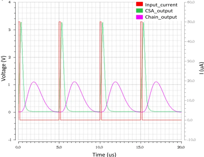
In order to improve the efficiency of the detection, a systematic study will be presented in the final paper. The aim will be to determine what are the threshold currents of the detector and also, what is the limit of detection of two consecutive currents. The electronic chain for signal conditioning has been simulated using Cadence (SPICE-based simulator). First results of simulation are shown in Fig. 2. In this preliminary simulation, the input pulse follows a
!"#$%$&'()*%+,-)++ .%/$%+! 01+ 23+ 03+ 4&)$5%()*%+3&/+.%/$%+ ! 21+ 26+ 06+ 07+ 08+ 09+ :,+ ;$&-*%+ ! 4&<=)>?=%%$&)+ 2@(%5$+;$&-"'A$+:B<C"D$%+ ! 2,+ 0,+ 2;:+ 2;:>*=)<=)+ ! 4&)$5%()*%+3&/+.%/$%+ ! 27+ 28+ 0E+ 0F+ 0,G+ 0,,+ :3+ 2@("&>*=)<=)+ !
rectangular shape (Input_current), what is sufficient for a first evaluation of the chain response. The CSA output together with the shaper output (Chain_output) are also depicted in Fig. 2.
Fig. 2: Transient response of the conditioning chain for successive pulses at constant
frequency (200 KHz).
Moreover, several solutions will be proposed to decrease pulse pile-up occurrence. Pulse pile-up happens when pulses arrives closer in time than the pulse resolution time for the system. Thus, in Fig. 3, the pile-up phenomenon is visible. The peak pulse of the output signal is 1.1V at the beginning of the process (before pile-up) and increase up to 1.33V as soon as the second pulse is detected. In the final paper, the input currents will be noise source currents modeled using the systematic tool SITARe [5]. In SITARe, the current model takes as input the ion physical characteristics (initial energy, LET, particle species) and location (point of generation, strike angle). The current modeling is based on a simplified drift-diffusion model. The model outputs are the currents generated at the sensitive zones of the pixel of detection, what are the outputs of the detection chain.
!"#$%&'$(()"%* +,-&.$%#$%* +/01"&.$%#$%*
2.
3%04
)*
52
6*
!*5
$-6*
718)*5$96*Finally, the association of the systematic tool SITARe with Cadence will provide a complete simulation platform, necessary for the characterization and the design of the full conditioning chain.
Fig. 3: Transient response of the conditioning chain showing pulse pile-up
(Frequency=572 KHz)
[1] K. Castellani-Coulié, H. Aziza, W. Rahajandraibe, G. Micolau, J-M. Portal, “Development of a CMOS Oscillator Concept for Particle Detection and Tracking”, RADECS 2012, Biarritz (France), 24-28 septembre 2011.
[2] Emilio Gatti “The Quest for Low-Loise Processing of Random Signals, Integrated Circuits, and Nuclear Science”, IEEE Solid-State circuits magazine, Volume 4, Issue 3, Summer 2012.
!"#$%&'$(()"%*
+,-&.$%#$%*
+/01"&.$%#$%*
2.
3%04
)*
52
6*
!*5
$-6*
718)*5$96*
[3] Vandenbussche et al. “Fully integrated low-power CMOS detector”, IEEE Trans. On Nucl. Sc., Volume 45, Issue 4, August 1998.
[4] Sven P.Bonisch “Current and charge sensitive signal conditioning for position determination”, Semiconductor Radiation Detection Systems, Sidney.
[5] G. Micolau, K. Castellani-Coulie, H. Aziza, J-M. Portal, “SITARe: a SImulation Tool for Analysis and diagnosis of Radiation Effects”, 12th IEEE Latin American Test Workshop, Porto de Galinhas, Brazil, march 27th-30th 2011.