Asynchronous Direct Digital Synthesis Modulator
Implemented on a FPGA
by
Jennifer H. Shen
Submitted to the Department of Electrical Engineering and Computer Science
in Partial Fulfillment of the Requirements for the Degrees of
Bachelor of Science in Electrical Science and Engineering
and Master of Engineering in Electrical Engineering and Computer Science
at the Massachusetts Institute of Technology
May 23, 1997
Copyright 1997 Jennifer H. Shen. All rights reserved.
The author hereby grants to M.I.T. permission to reproduce and
distribute publicly paper and electronic copies of this thesis
and to grant others the right to do so.
Author
Department of Electrical Engineering and Computer Science
May 23, 1997
Certified by
fessor James Kirtley Jr.
, hesis Supervisor
Accepted by
-
.
... 'ur
C. Smith
Chairman, Department Committee on Graduate Theses
Asynchronous Direct Digital Synthesis Modulator Implemented on a FPGA
by
Jennifer H. Shen
Submitted to the
Department of Electrical Engineering and Computer Science
May 23,1997
In Partial Fulfillment of the Requirements for the Degree of
Bachelor Science in Electrical Science and Engineering
and Master of Engineering in Electrical Engineering and Computer Science
ABSTRACT
As IC chips get faster and smaller, the synchronous design method has hit
upon the limitations of clock skew, higher power dissipation, and timing
verifications. Now asynchronous design is being used to overcome those
boundaries. It relies on request / acknowledge signalling instead of clock
driven operation. This project will implement an asynchronous direct
digi-tal synthesis modulator which does quadrature phase-shift keying. Two
data streams, I and
Q,
are passed through interpolation filters. The
numeri-cally controlled oscillator (NCO) takes in a set frequency and generates
sine and cosine waves which are then modulated with the two filtered data
streams respectively. The two waves are recombined for a final output to an
external digital-to-analog convertor. Given the limited time frame, the
sys-tem will be programmed on a field programmable gate array (FPGA) using
VHDL programs that simulate the different blocks. The FPGA will be
tested to verify the functionality of the asynchronous design. The focus of
this thesis is on the asynchronous techniques developed.
Thesis Supervisor: Professor James Kirtley Jr.
Title: Professor of Electrical Engineering
Company Supervisor: Dr. John Grosspietsch
ACKNOWLEDGEMENTS
Thanks to Prof. James Kirtley, Jr. for being my thesis advisor.
My thanks to the engineers at the IC Design Lab at Motorola
Chicago Corporate Research Labs and my manager Steve Gillig.
Special thanks to Tim Rueger for all his help.
To all those special people that kept me sane and motivated:
Edward Hwang, Nitin Kasturi, and Erica Pearson.
I would like to extend my sincerest appreciation to my company
supervisor Dr. John Grosspietsch without whom there would not be
any thesis.
Finally, I dedicate this work to my parents, Robert and Julia Shen
for all their support.
TABLE OF CONTENTS
1.
Introduction
...
...
...
9
2.
B ackground ... ... ... 10
2.1
Request/Acknowledge Signalling ... 10
2.2
Micropipelines ....
...
14
2.3
Self-Timed Circuits ... ...
15
3 .
D esig n ...
17
3.1
P urpose ...
...
17
3.2 Direct Digital Synthesis Modulator... 17
3.2.1
G eneral D escription ...
17
3.2.2
Asynchronous Design Decisions ...
...
18
4.
Im plem entation of M odules...21
4.1
Control Signalling ... . ... 21
4.1.1
Com pletion Elem ents ...
21
4.1.2 Four Phase HandShaking Elements and Registers ... 23
4.1.3 Delay Insertions ... 23
4.2
Self-Timed Blocks ...
...
24
4.2.1
Self-Tim ed Adders... 24
4.2.2
Self-Timed Multipliers ... 25
4.3
Sine and Cosine Wave Generation...26
4.3.1
Numerically Controlled Oscillator ...
... 27
4.3.2
Sine and Cosine ROMs...29
4.4
Interpolation Filters ...
33
4.5
Input Data Generation: Quadrature Phase-Shift Keying ... 34
4.5.1
QPSK Rotation ...
... 34
4.5.2
Random QPSK ...
35
4.5.3
Integration of the Two QPSK Methods ...
...
36
5.
Software and Hardware Configurations...38
5.1
Softw are D esign Flow ...
38
5.2
FPGA Demonstration Board Setup ... 40
5.3
Digital to Analog Convertor Board Setup ... 42
6.
R esults and Verification ...
44
6.1
DDS Outputs: Sine and Cosine Generation...44
6.2
Q PSK ...
... 46
6.3
Random QPSK ...
...
4...
8
6.4
System Observations ...
49
7 .
C onclu sion ... 50
References ...
... ... 51
Literature ...
...
51
W eb Sites ...
...
51
A ppendices ...
...
... 53
V H D L Code for M odules ... 53
LIST OF FIGURES
1.
Request Acknowledge Signalling ...
10
2.
Tw o-Phase Signalling.. ...
11
3.
Four-Phase Signalling ...
11
4.
C-element and Example ...
...
12
5.
Four-Phase Handshaking Circuitry ... 13
6.
Different Cases of Four-Phase Signalling Inputs and Outputs ... 13
7.
Micropipeline Structure From Sutherland's Paper [4] ... 14
8.
D C V SL Logic ...
... . . 16
9.
DCVSL Blocks with Control Blocks ...
16
10. Block Diagram for the Direct Digital Synthesis Modulator ... 18
11.
Block Diagram of the DDSM With Asynchronous Control Paths... 19
12. D esign Flow ...
. . ... 20
13. Simplified Block Diagram of XC4000-Series CLB...21
14. Gamble C-element and Truth Table [6] ...
22
15. Gamble's C-element Signals ...
22
16. Combinational C-element with the Y Input Inverted and Truth Table ... 23
17. Pipeline Control ...
. 23
18. Optimized C-element Acting as a Delay Element ...
24
19. Self-Timed Adder...
25
20. Self-Tim ed M ultiplier ... 26
21.
Wavetable ...
... 27
22. Frequency Step Input to ROM s...
27
23. NCO Schematic with Delay Insertions ...
28
24. Sine W ave Breakdown ...
...
29
25. Sixteen Point Sine W ave Beginning at Zero ... 30
26. Sixteen Point Sine Wave With Offset ...
31
27. 256 Point Sine Wave with Zeros and No Zeros ... 31
28. Sine and Cosine Generation Schematic with Delay Insertions ... 32
29. Interpolation Filter Schem atic...33
30. Matlab Generated Z-transform of Interpolation Filter...34
31. QPSK Clockwise and Counterclockwise Rotation ...
35
32. Schematic of Pseudorandom Generator ...
36
33.
QPSK schematic with Interpolation Filters ... 37
34. FPGA Demonstration Board Schematic ... 41
35. FPGA Demonstration Board Physical Layout ... 42
37. Generated Sine and Cosine W aves at 1.8 M Hz...
...
44
38.
1024-PT FFT vs. 78-PT FFT Carrier Frequency For Case A...
45
39. Polaroid Showing the Generated Carrier Wave Spectrum ...
45
40. Theoretical Output Spectra of the CW and CCW for Case A ... 46
41. Leading and Lagging First and Third Harmonics ... 47
42. Matlab Generated Spectrums of the QPSK output CW, CCW ... 47
43. Polaroid Showing the Spectrums of the QPSK output CW, CCW...48
LIST OF TABLES
1.
Gamble C-Element W ith Y Inverted...22
2.
Com binational C-Elem ent...
23
3.
Tim ing of Delay Elem ents ...
24
4.
Partitioned Design Utilization Using Part 4010EPC84-2 for DDSMQPSK.VHD...40
Chapter 1. Introduction
While the synchronous approach has helped to simplify the design of IC chips, the limitations are becoming more evident as technology get smaller and faster. Each pass to increase the system clock for a higher throughput requires a redesign and re-verification of the full synchronous system, while the faster switching action dissipates more power throughout. We are gaining higher performance at the cost of higher power and longer re-design time [1]. Since synchronous design became popular, asynchronous research is now being revived to overcome those boundaries.
The lack of a global clock is the one trademark which separates asynchronous from its counterpart. Without any clocked circuits, there will be less switching which implies, but does not guarantee less power dissipated in the circuit. Another favorable condition is that the redesign becomes more modular. When a module is replaced by a faster one, there's no need to recheck timing parameters. Each module operates at its own pace whether fast or slow. When done, the module signals the next subsystem.
This thesis utilizes the asynchronous pipeline methodology to implement a digital system. In this case, a direct digital synthesis modulator is the proposed system. Given the fact that no commercial asyn-chronous standard cell libraries or asynasyn-chronous field programmable gate arrays (FPGAs) are available, we are limited to synchronous FPGAs. The time frame for this project is too short to develop a standard cell asynchronous library from scratch which would be more satisfactory. The focus of this thesis is the asyn-chronous techniques developed for this project. The resulting project is to be tested for functionality of the asynchronous system and the use of self-timed modules.
Chapter 2 provides the background material about asynchronous research applicable to this thesis. Chapter 3 proposes the design to be built. Chapter 4 presents goes over the work done and the decisions made for each block. While Chapter 5 discusses all the relevant software issues and hardware specifications for the FPGA, the demonstration board, and the digital-to-analog convertor. Chapter 6 covers the testing and verifying the functionality of the system with concluding remarks in Chapter 7. References and Appendices are located at the end of this thesis.
Chapter 2. Background
Asynchronous design has been around at least since the 1950's, but it was displaced in favor of syn-chronous techniques. [3] Present day limitations in synsyn-chronous design have marked a revival in asynchro-nous research. There are many branches to this field, but the one common trait to all of them is the absence of a global clock.
2.1 Request/Acknowledge Signalling
Without the clocks, the modules communicate using request/acknowledge signalling. For example, one module finishes and fires a request signal to the next one. It receives the request and grabs the valid data from the module or the bus. When finished, the receiver fires off an acknowledge to the sender module indi-cating that the transfer is complete. The modules goes into a stand-by mode which uses no or little power while waiting for the next request. [4] See Figure 1 for basic setup.
FIGURE 1. Request Acknowledge Signalling
There is one protocol that is adhered to. The data being passed to the receiver must be held valid from when the request fires until the acknowledges fires in return. There are two main types of request/acknowl-edge signalling: two-phase signalling [4,12] and four-phase signalling[4,11].
Two-phase signalling is based on event triggering. A rising or falling edge are both considered to be events. The request event is always answered by a acknowledge event after some indeterminate delay. The sender and receiver must wait for those events. Since both rising and falling edges are crucial in signalling, the resulting circuitry must be hazard free and delay insensitive. A hazard in the control circuitry will cause errors to result. See Figure 2 below. Valid data appears on the sender's outputs. The sender signals an event on the request line. (1) The receiver latches the valid data and responds with an event on the acknowledge wire. (2) The sender gets the acknowledge event and waits for the next request. Note that the data can become invalid after the acknowledge event (3).
Request
Acknowledge
Data
I I
One Cycle ---- 6 - Next Cycle "
FIGURE 2. Two-Phase Signalling
Four-phase signalling requires that the request and acknowledge line must return to logic zero after each handshake as shown in Figure 3 below. The first step is for the sender to wait for data to become valid. The request line is pulled to logic one causing the receiver to work on the incoming data. (1) When done, the receiver pulls its acknowledge line high. (2) After this, the sender pulls it request line back to logic zero. (3) Answering in kind, the acknowledge line is pulled down. (4) This protocol has two transitions per signal for each communication. Four-phase signalling is easier to implement from a circuit standpoint. Logic for two-phase signalling is far more complex since both rising and falling transitions must trigger the same events.
Request 1 2
I1' 3 44
Acknowledge
Data valid / /// valid / // valid
One Cycle - I
FIGURE 3. Four-Phase Signalling
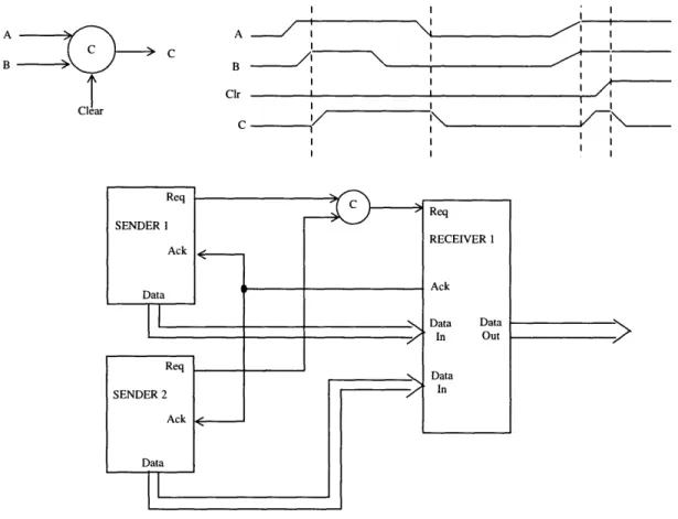
One basic building block of asynchronous control signalling is the completion element (C-element). These C-elements are important for the control signalling between blocks. Without the clocks, the control signalling circuitry must be asynchronous and be able to wait indefinitely for single or multiple events [4]. A single C-element can have two or more inputs and one output. When all the inputs are logic one, then the output will be logic one. When all the inputs are logic zero, then the output will be logic zero. If all the inputs are not the same, the output remains the unchanged. In addition, a clear input pulls the output down to logic zero. A C-element and its timing diagram are shown in Figure 4.
The C-elements are used to signal the completion of multiple modules. An example is shown in the bottom half of Figure 4. Two sender modules each have a request line, an acknowledge line, and a data port.
A C-element can be used to synchronize the two requests to the receiver module. The acknowledge signal resets both sender modules once the receiver is done.
A JarL I I I
A
B Or I cFIGURE 4. C-element and Example
C-elements should be built at the transistor level. Building a C-element with only gates can lead to meta-stability issues, and hazards can result. Hazard-free C-elements are definitely needed for asynchronous design. Any hazards caused in the control signalling can lead to false data being transferred between mod-ules. Building C-elements on the transistor level is more ideal than using just logic gates. However for this thesis, the field-programmable gate array hinders us in that respect. Section 4.1.1 gives more details about the specific C-elements used for this project.
As shown above, one C-element can implement two-phase handshaking. Four-phase handshaking ele-ments can be built out of C-eleele-ments. Figure 5 shows a four-phase handshaking structure. Notice that one of the inputs is inverted going into each C-element. The two C-elements have two handshaking pairs- (1) Reqln with AckOut and (2) ReqOut with AckIn. Reqln and AckIn are two inputs; ReqOut and AckOut are two out-puts. The four-phase handshaking element is often used in pipelined structures [5].
Reqln
C
RC
>
ReqOut
Reqln
4HS
I ReqOutAckOut ::I r-ý AckIn
FIGURE 5. Four-Phase Handshaking Circuitry
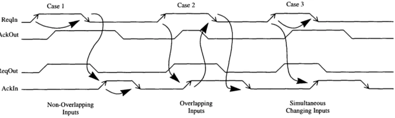
The four-phase handshaking element is used to handle the request and acknowledge signaling between modules. Each request/acknowledge signal pair must follow the data valid protocol. Whether data is being sent or received, the data lines must remain valid between the request event (rising only) and the corresponding acknowledge (rising only). Below are three cases of possible inputs and output combinations for Reqln, AckOut, ReqOut, and Ackln. Notice that the request/acknowledge pairs are following the four-phase handshaking protocol. See Figure 6 for signalling details.
Case 1 Case 2 Case 3
Reqln
AckOut
ReqOut
AckIn
Non-Overlapping Overlapping Simultaneous
Inputs Inputs Changing Inputs
FIGURE 6. Different Cases of Four-Phase Signalling Inputs and Outputs
This asynchronous element must work correctly for all possible input combinations. Case 1 shows the inputs as non-overlapping. Reqln goes high which pulls AckOut and ReqOut high. Reqln falls before the AckIn is pulled high. Afterwards, both AckOut and ReqOut are pulled low. This case shows that Reqln and AckIn are non-overlapping when high. Case 2 shows the inputs overlapping. When Reqln is pulled high, then Ackln is pulled high afterwards. Reqln is then pulled low followed by AckIn pulled low. This shows that Ackln and Reqln are pulled high at different times and overlap. The last case shows the inputs changing simultaneously. Reqln is pulled low at the same time AckIn is pulled high. These different cases show the hardiness of the four-phase signalling element for all different input combinations. Notice how the ReqOut and AckOut respond to the different cases. Control structures such as these are crucial for asynchronous design. Hazards must be checked for carefully.
2.2
Micropipelines
Pipelines are used to speed up the throughput of a repetitive process. Combinational logic is separated by clock driven registers, and the data flows through each stage. Ivan Sutherland modified a standard line by replacing the clock signaling with request/acknowledge signalling. He called these modified pipe-lines "micropipepipe-lines". Figure 7 show more detail. These micropipepipe-lines used C-elements to signal between the stages, while event driven registers control the flow of data [4,7].
FIGURE 7. Micropipeline Structure From Sutherland's Paper [4]
The R(in) signal which stands for Request In triggers the pipeline. As the control signals propagate down the pipeline, the data is pushed through it. The two-phase signalling structure is accommodated by event driven registers (capture-pass) as seen in the figure. When the capture input (C) gets an event, the D(in)
which is Data In is latched into the pipeline. The capture done (Cd) output from the register is delayed to the next C-element. When the pass input (P) is triggered, the latched data is transferred to the outputs. Pass done (Pd) is then fired. The combinational logic between the stages must finish before the capture signal of the next stage fires. In Figure 7, note the inserted delays between the C-elements.
For the micropipeline to work correctly, the delay through the C-element must be greater than the propagation delay through the registers and the propagation delay through the combinational logic [4]. The data must be valid going into the next stage before the request signal fires. Inserting delays are necessary for
TpdC> TpdR + TpdL
TpdC propagation delay through C-element
TpdR propagation delay through register
TpdL propagation delay through combinational logic
Sutherland's inserted delays are a drawback in some cases. Some circuit optimizers (i.e. FPGA com-pilers) will remove the inserted delays. Without these delays, the wrong data will be latched from stage to stage. The inserted delays keep the control signalling from reaching the register too fast. If the logic between registers is still computing when the control signal reaches the register, invalid data will be capture and sent on to the next stage. This invalid data would certainly corrupt the rest of the systems output. This possible complication stresses the importance for inserted delays. However, inserted delays need to be re-verify each time the logic is changed in the data path which adds to the re-design time. What is really needed is a com-pletion signal from the combinational logic so that inserted delays become unnecessary for the designer.
2.3 Self-Timed Circuits
Self-timed circuits follow a request/acknowledge protocol. The request signal enables the circuit to evaluate its inputs. When the evaluation is done, the circuits pulls its acknowledge signal (completion or done signal) high. A self-timed circuit should be able to wait indefinitely for the request signal to activate. It does not need a clock edge for timing. This type of circuit is valuable for asynchronous design where delays are assumed indefinite.
Sutherland's micropipeline relied on inserted delays between C-elements to insure the correct opera-tion of the pipeline. Using self-timed circuits in an asynchronous pipeline will eliminate the need for these inserted delays. The completion signal for the self-timed circuit indicates when the logic is finished evaluat-ing. This "done" signal can be integrated into the control structure so that each stage waits for the comple-tion signal before continuing. See Figure 9 for details. Without the need of inserted delays, this will simplify the work for the asynchronous logic designer.
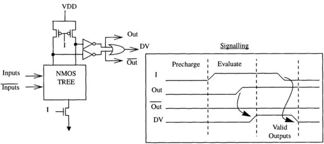
One type of self-timed circuit is the differential cascode voltage switch logic (DCVSL). This transis-tor logic follows a precharge and evaluate style (dynamic logic). It has a request input (I) and a data valid output (DV). These signals follow a four-phase signalling protocol with differential inputs and outputs. When I is low, the pfets are turned on, and the internal nodes are both pulled up high. While Out and OutBar are both pulled low. When I goes high, the NMOS logic tree evaluates and pulls one of the nodes low. The DV signal goes high when one of the outputs is pulled low [5]. See Figure 8 for a transistor description.
VDD Out Signalling Inputs Inputs I'-] FIGURE 8. DCVSL Logic
All the combinational logic is laid out in N-fets in the NMOS tree. Four-phase signalling modules are needed to control the DCVSL structure. Inputs into the NMOS tree must remain valid while I is high. If no registers were inserted between the stages, then previous stage (j-1) would have to remain static while the current stage (j) evaluated. The following stage (j+1) would be precharging [8]. Inserting registers in between cuts down the number of stages. Figure 9 shows registers that have been inserted between the DCVSL blocks [5]. Notice how the I (request) and DV signals are integrated into the control structure.
Reqln AckOut
FIGURE 9. DCVSL Blocks with Control Blocks
The registers do not need to signal when the data is latched. This system assumes that the propagation delay of the register is smaller than the propagation delay through the interconnect circuitry. The registers do not follow the request acknowledge protocol but depend on inherent delays of the circuitry.
I Out Out DV L .1 I I
Chapter 3. Design
3.1 Purpose
Since most IC design efforts are directed toward synchronous design, the available software tools reflect that trend. Presently, there are no commercial tools for designing asynchronous systems. Only univer-sities have developed the software to analyze and synthesize asynchronous circuits [9]. To do a fully self-timed IC design can take a few years to build, due to a lack of commercial asynchronous standard cell librar-ies. Since this thesis project has only a few months to be completed, we must utilize what technology we have. We implemented an asynchronous system on a field programmable gate array (FPGA) which was orig-inally made for synchronous designs. There was some skillful manipulation of the software for this work to be accomplished.
The purpose of this thesis was to build an asynchronous direct digital synthesis modulator. We used current research to develop a functional design in a short timeframe. The FPGA implementation was to
ver-ify the correctness of the work. The research has taken different asynchronous techniques and combined
them into a more workable methodology. Self-timed circuits and Sutherland's micropipelines were applied with the minimal use of inserted delays. Hopefully, the resulting asynchronous techniques can be used to implement a full custom IC, and other self-timed designs can be functionally tested on the FPGA.
3.2 Direct Digital Synthesis Modulator
This Section 3.2.1 contains a general description of the direct digital synthesis modulator (DDSM) without the asynchronous modifications. Section 3.2.2 elaborates on making the DDSM into a self-timed pipeline and the design-flow to accomplish this transformation.
3.2.1 General Description
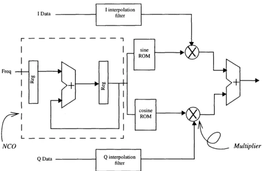
A DDSM modulates data onto carrier waves. Figure 10 shows a general block diagram of the system.
It synthesizes sine and cosine waves at a programmable frequency using numerically controlled oscillator
(NCO). The I and Q data streams can be analog signals converted to digital. Or they can be digitally
gener-ated waveforms from other chips. The I and Q data streams are put through interpolation filters to match the sampling rate of the system [13]. Each filtered data stream is multiplied by the sine and cosine wave respec-tively. The outputs are added together for the resulting modulated waveform. An external digital-to-analog convertor converts the bitstream to an analog signal. Note that the block diagram does not show the asyn-chronous control paths. The asynasyn-chronous version of DDSM appears in the next section 3.2.2.
Freq
NCC
FIGURE 10. Block Diagram for the Direct Digital Synthesis Modulator
The DDSM system can be used for digital signal processing applications. It shifts the baseband data to the carrier frequency for transmission over a communications channel [15]. The addition of the two mod-ulated signals can incorporate two independent data streams in the same bandwidth called quadrature-ampli-tude modulation [15]. One such example is quadrature phase-shift-keying (QPSK). I and Q change between
+/-1 which cause the resultant phase shifts of +/- PI/4 and +/- 3*PI/4. These four phase shifts represent the
four different bit combinations of I and Q (00,01,10,11). A more detailed theoretical description of QPSK is written in Section 4.5.1.
Currently, the commercial synchronous counterparts runs at about 100 MHz to 150 Mhz on average with range of 300 mWatts to 500mWatts. Since we are implementing on a FPGA, the system throughput and power was not expected to match up. However, the functionality of the design can be checked with this implementation.
3.2.2 Asynchronous Design Decisions
After researching different asynchronous techniques, a four-phase handshaking protocol was chosen to be implemented for this design. The last stage in the pipeline has its Rout and Ain tied together which resets all the control signals going back up the pipeline. This method has similarities to Sutherland's micropipeline [4] discussed in Section 2.2. For example, a single Rin event propagates one valid data point to the end of the pipeline while the acknowledge line resets the system. Whereas a synchronous pipeline with M stages needs at least M clock pulses to get a valid data point out. Also, the asynchronous pipeline can wait indefinitely for the next event instead of requiring a constant clock. Asynchronous pipelines are good for applications which have indeterminate periods of waiting between calculations. Unfortunately, the
DDSM system must operate continuously for signal modulation which requires an external clock driving the Rin input to the pipeline.
As with pipeline architecture, there are registers between each stage which are triggered by the acknowledge line. Each block is attached to the respective control signals to the blocks preceding and suc-ceeding. This connection determines when a stage can operate depending on the operational state of the blocks next to it. Making the blocks self-timed can benefit the design since the FPGA compilers can opti-mize out set delays (i.e. double inverters). Ultimately, the multipliers and adder are self-timed, while the NCO and ROM's use inserted delays. Figure 11 shows the DDSM block diagram adapted to asynchronous control signals. Request Line Freq NCO Rin SAout L- -External Function Generator Q
I Combinational Register Self-Timed Cell Register I Logic
I with Inserted I Delays
FIGURE 11. Block Diagram of the DDSM With Asynchronous Control Paths
The Xilinx XC4010E FPGA was chosen to implement this asynchronous system. This FPGA is a SRAM based family with look-up tables in each combinational logic block (CLB). The bigger the FPGAs are, the more CLBs are inside the hardware. The added CLB's allow for more complex designs and/or more bitwidth. With the XC4010E FPGA, there are 400 CLB's to be utilized.
The different blocks of the system are programmed and simulated in VHDL. Each module is com-piled and simulated in QuickVHDL. Once the VHDL blocks are working, they are synthesized to logic gates by using Synopsys Design Analyzer (SDA). Synopsys is a software package which reads in VHDL and syn-thesizes the gate-level design. However, Synopsys takes a limited subset of VHDL commands. If a program
is unreadable by the design analyzer, the VHDL must be rewritten and retested until it can be read by Synop-sys. The generated gate-level schematics are compiled into the netlist code for the FPGA software (XACT).
Once th, XC4010E part is programmed, it is placed on a pre-made FPGA demonstration board. The digital inputs and outputs are tested for correct functionality. An external digital-to-analog device converts the output into a continuous signal for the spectrum analyzer. The design flow can be seen in Figure 12. Note the Design/Testing abstraction line.
4
(Theoretical) rlertflrumLfnrf
Design Flow Simulation
FIGURE 12. Design Flow
Obstacles and stumbling blocks are inherent to any large design. One particular software problem was compiling the VHDL programs through different software tools. For example, Synopsys only takes a subset of VHDL so some experimentation is required for correct programming. In addition, XACT (Xilinx's design editor software) must be able to read in the files generated from Synopsys. Another design problem was syn-thesizing the self-timed circuitry to the gate-level. In this case, transistor level design is desired but impossi-ble to do on a FPGA which employs look-up taimpossi-bles and combinational logic.
A potential hardware problem is the size of the FPGA. The pre-made demonstration board can only take an 84 pin package. This restriction limits the size of the FPGA we can use. The largest FPGA for the 84 pin package was the XC4010E part. If the design exceeded the 400 CLBs, then we would need two demon-stration boards to fit the project. Using two boards might limit the throughput of the pipeline since the largest delays are through the pads. An additional problem is disengaging the clock drivers to the edge-triggered flip-flops in the FPGA since the design calls for no global clock signals. Thankfully, all these problems were overcome in a short period of time [10].
Chapter 4. Implementation of Modules
The asynchronous system can be broken down into several different stages. Each section describes a particular module in detail. Theoretical calculations are also included when relevant unless otherwise noted. The VHDL code for all modules is located in Appendix.
4.1 Control Signalling
4.1.1 Completion Elements
Completion elements are used to handle the request/acknowledge signalling in the asynchronous pipeline. The basic function of C-elements was described in Section 2.1. For this design, multiple C-ele-ments are needed for control signalling and delay eleC-ele-ments. However, the FPGA has a limited number of logic gates. The Xilinx FPGA is made up of combinational logic blocks (CLB). The amount of CLBs in an
FPGA limits the size of the design that can be downloaded into the hardware. By designing the C-element to
fit in one Xilinx CLB structure, this will ultimately conserve logic gates.
Figure 13 shows the internal structure of a CLB [14]. The logic functions of G' and F' are SRAM lookup tables for up to 4 inputs, while logic function of H' is for 3 inputs. These function generators imple-ment all the combinational logic in a design. Internal multiplexors select the various outputs of G', F', H', or other outputs to go through flip flops X and Y. Flip flops X and Y are clocked on the same signal (inverted or not inverted).
Note:
Note: kI
M. Gamble at the University of Manitoba, Canada constructed a micropipelined multiplier in a Xilinx XC4003 FPGA[6]. Their multiplier project included the design of a C-element with one inverted input which fit into one Xilinx CLB. Figure 14 shows the Gamble C-element and its truth table [6]. The three gates labeled A, B, and C map into the SRAM function generators G,F, and H respectively. Feedback outside the CLB loops the Z signal to the clock signal of the flip flops. One flip flop is used for this C-element. Since both flip flops in a CLB are clocked on the same signal, the second flip flop is unused.
TABLE 1. Gamble C-Element With Y Inverted
Y Tr
FIGURE 14. Gamble C-element and Truth Table [6]
Gamble's C-element has the Y input inverted. The inverter and flip flop causes the flip flop to toggle between logic 1 and logic 0 whenever the Tr goes high. When X and Y are opposites and Z is opposite from X, the Tr signal goes high which clocks the register. The Z flips and Tr is pulled low immediately afterwards. The C-element then waits for its next input change. This Tr pulse is represented in Table 1 as the up and down arrows. The rising edge flip-flop in the CLB needs Tr reset to zero before the next possible input change. If the inputs do change while Tr is still high, the CLB may not work correctly. This hazard in Gam-ble's C-element is avoided by the four-phase handshaking configuration which we are using. Figure 15 shows the Gamble's respective signals for different possible situations.
Hold Z
X= 1, Y=1
I
I
o
x
Y
o
..
FIGURE 15. Gamble's C-element Signals
X -Y Tr Z(n+l)
0 0 0 Z(n)
1
0
1
A C-element with the Y input inverted made with only combinational logic and asynchronous feed-back was placed through the design flow for comparison. The straight combinational logic in Figure 16 took up 2 CLBs per C-element. With four phase handshaking and 2 C-elements per stage, we would have used up twice as many CLBs. For this primary reason, the Gamble C-element was used in this thesis.
TABLE 2. Combinational C-Element
X -Y Z(n+l)
0 0 Z(n)
0
1
0
1 0 1
1 1 Z(n)
FIGURE 16. Combinational C-element with the Y Input Inverted and Truth Table
4.1.2 Four Phase HandShaking Elements and Registers
Generic four phase handshaking elements were described in Section 2.1. This four-phase element was built with two Gamble designed C-elements (Fig. 5) with a reset input. The reset input connects to the clear input to each C-element. The Aout signal from the four phase handshaking element is used to clock the pipe-line registers. Figure 17 shows the pipepipe-line control configuration with a combinational logic block between stages. Inserted delays are present if the combinational logic is not self-timed.
Rir Aol
Rout Ain
FIGURE 17. Pipeline Control
4.1.3 Delay Insertions
Delay insertions are a necessary part of asynchronous pipelines. Inserting buffers would act as delay elements in the design. However, the Synopsys software would optimize out double inverters and buffers. Instead, we inserted Gamble C-elements with their inputs tied together to act as delay elements. Synopsys does optimize the C-element, but does not eliminate it entirely. Figure 18 shows the optimized C-element
with its inputs tied together. The table shows the experimental delay times through one and more delay ele-ments in series using the Xilinx FPGA architecture.
TABLE 3. Timing of Delay Elements
REG Out
In CLR
Reset
FIGURE 18. Optimized C-element Acting as a Delay Element
4.2 Self-Timed Blocks
There are two independent paths in an asynchronous pipeline system. One path is for the data being manipulated and the other path is for the handshaking signals. Normally with delay insertions only, the con-trol path is independent of the data path. However with the self-timed architecture, the two paths become dependent on each other. The request/acknowledge (I/DV signals) protocol imposed on the logic blocks are used to break the abstraction. The I and DV signals complete the handshaking connection between each 4-phase handshaking module. See Figure 9 in Section 2.3 for illustration of concept. The self-timed architec-ture can be referred to as the "data-driven architecarchitec-ture" [16], since the combinational logic now controls the speed of the asynchronous pipeline.
4.2.1 Self-Timed Adders
The VHDL language allows adders to be inferred from the "+" sign. Synopsys reads the VHDL code and instantiates the appropriate adder. We used these instantiated adders to create a timed adder. A self-timed adder sums its addends only when the request input (I) is high. The sum is only valid when the data valid signal (DV) goes high. Self-timed circuits make inserted delays unnecessary. In transistor logic, a self-timed circuit is simpler to implement. However for gate level design, it requires more logic to build.
Two adders are used to build one self-timed adder. One adder sums the addends; while the other adder computes the inverse sum. For example, if 0011 and 0010 were added, the sum would be 0101; while the inverse of sum would be 1010. When I is high, one set of inputs is inverted and Cin is pulled high. This cal-culates the inverse sum. The sum and inverse sum bits are checked using exclusive OR's which then gener-ates the data valid completion signal. When I is low, inputs to both adders are initialized so that the sum and inverse sum are both zero which in turn re-initializes DV to zero. Figure 19 shows a 4x4 self-timed adder. This configuration is easily adapted to a higher bit width.
Number of Propagation C-elements Delay 1 11.8ns 2 24.92 ns 3 28.56 ns 4 40.46 ns
A I
B
I (Enable) DVSum
0 A/777777777+J77\ 0FIGURE 19. Self-Timed Adder
4.2.2 Self-Timed Multipliers
From the VHDL language, the "*" sign infers multipliers. Synopsys reads the VHDL code and instan-tiates the appropriate multiplier. By specifying the integer ranges of the multiplier and multiplicand, Synop-sys interprets an unsigned binary multiplier versus a two's complement multiplier.
The instantiated multipliers are used to create a self-timed multiplier similar to a self-timed adder. Two multipliers compute the product and its inverse product. One multiplier has inverters on its output to compute the inverse product. The self-timing mechanism is created by initializing the inputs to a specified output. When the enable (I) signal is low, the data valid signal must be low (DV). When I is high, the product and inverse product are exact opposites in bits. Exclusive or's compare each bit and generates the DV signal. The inputs are set up that when I is low, the outputs of the two multipliers will be the same. When I goes high, the outputs are inverted and the DV signal goes high. Figure 20 shows the implemented self-timed multiplier.
A I B I (Enable)
DV
Product 0 0A*BFIGURE 20. Self-Timed Multiplier
The inputs going into the top multiplier are conditioned using AND gates; while the inputs going in the bottom multiplier are conditioned using AND gates and OR gates with one inverted input. When I is low, the top multiplier calculates OxO=0 while the bottom multiplier calculates lx(-1)= -1. Since the bottom mul-tplier's output is inverted, inverse product are all zeros. The top multiplier are also all zeros. This initializes the data valid (DV) signal to zero. When I goes high, 9-bit A and 4-bit B inputs are passed into the multipli-ers. When the calculation is completed, the products are inverses of each other and DV goes high. The bot-tom half of Figure 20 shows the pertinent signals.
For this self-timed implementation, we need the DV signal to be hazard free since it connects to the Rin input of the next stage. The hazards can result if the 13-bit product and inverse product match up as opposite bits during the calculation before the final product is completed. This causes the exclusive OR to pull high prematurely which in turn creates a hazard on the DV line. The long length of the bitword and the exact timing for each multiplier makes it less hazard prone, although the possibility is still there.
4.3 Sine and Cosine Wave Generation
The sine and cosine wave generation comprise about one-third of the overall system design. The pro-grammable frequency allows the user the freedom to adjust the waveform immediately.
A section of memory can hold all the values from a single waveform. By sampling that table
repeat-edly, you can get a periodic waveform. Take a sine wave for example. If you take every value from the table, you get a complete copy of the waveform. Skipping every other point in the ROM will produce a sine wave that is half the length of the original. The more points that are skipped, the higher the frequency is of the
resultant sine wave. Figure 21 illustrates this property [W4]. This straight-forward method can easily be implemented in digital logic.
Exact Copy
WAVETABLE OUTPUT
SSamples Skipped = Higher Frequency
WAVETABLE - VALUES USED OUTPUT
FIGURE 21. Wavetable
Section 4.3.1 describes the theory and implementation of the numerically controlled oscillator which accesses the waveform ROMs; while section 4.3.2 details the loading of the ROM's and its implementation in the FPGA. Both sections discusses the asynchronous implementation of each part.
4.3.1 Numerically Controlled Oscillator
The numerically controlled oscillator (NCO) runs through the samples in the wavetable. Its output serves as the address into the ROMs. Similarly, it represents the 0 to 2*PI index for the waveforms. Skipping addresses in the sequence is similar to counting in bigger increments to 2*PI. The NCO is an adder and an accumulator. Depending on the bitwidth (M bits) of the NCO, the number of frequency steps between 0 to 2*PI varies by 2AM. The lowest bitword maps to 0, while the highest bitword maps to 2*PI. The adder will eventually start back at zero when the most significant carry changes. The output of the NCO inputs to the cosine and sine ROMs. This generates cosine and sine waves at that particular frequency. Figure 22 shows a graphical depiction.
Waveform Representation of the Digital Waveform Representation of the Digital Output Bits of the NCO Output Bits of the Waveform ROMs
2*PI = Maximum Bit Word
F--' 0 = Minimum Bit Word
Finer frequency control was added to the system by increasing the bitwidth of the adder and taking the higher significant bits off the accumulator. Theoretical calculations were done to predict the frequency step and the minimum and maximum frequency of the NCO. Frequency inputs bits can be offset into the adder by A bits. And the NCO output bits are offset from the accumulator's LSB bits by B bits. The accumu-lator is clocked at a certain Rin frequency. These parameters combine in Eq. 2 to determine the current fre-quency of NCO based on the frefre-quency input bitword with 8 bits for the NCO output. One can determine the smallest frequency step of the system by setting F = 1. Setting F to the maximum bitword allowed gives the highest frequency. For example, if the frequency input has 8 bits, then setting F to 255 will determine the highest output frequency for the NCO.
Rin F
NCOfreq 2(8+B-A) (EQ 2)
where:
Rin clocking frequency of the accumulator F value of frequency step bitword
A number of offset bits of frequency bitword into adder B number of offset bits of the NCO output from accumulator
Based on the above equation, a particular NCO was determined for a frequency range about 1 MHz with a 5-10 kHz minimum increment. The design has a 8 bit frequency input choosing Rin to approximately be around 10 MHz. A and B were chosen to be 0 and 3 respectively in order to meet the design criteria. For this particular configuration, the theoretical minimum frequency step is 4.88 kHz, while the theoretical fast-est frequency will be 1.245 MHz. Experimental results should match these calculations. At the slowfast-est fre-quency, the NCO will make a 256 point ROM into a 2048 point waveform. Figure 23 shows the NCO design. The adder's 2 input MSBs are tied to logic 0.
A =0 since input I matches up with t adder's LSB Frequency Input Ri A( Selecting A Subsection Of Bits Off A Bus
(LSB -> 0) <5:2> / <3:0> 6 4 retical Calculations quency Step = 4.88 kHz Frequency = 1.245 MHz 10 MHz A=0, and B=3. Reset
FIGURE 23. NCO Schematic with Delay Insertions
Two Gamble C-element delays are inserted in the control signal pipeline for the NCO stage. We want this stage to regularly output addresses to the sine and cosine ROMs. The NCO is the first stage of the pipe-line and we want it to keep up with the external function generator which is driving the pipepipe-line. Ideally, the
Rin signal must rise when the Aout signal goes low which follows the four-phase handshaking protocol. But to have sine and cosine generation, we need the accumulator clocking at a set speed, which requires the need for an external clock. Placing an external function generator on the Rin input regulates the NCO output. It is assumed that Rout, Ain, and Aout will trigger around the Rin signal so that the four-phase protocol is satis-fied.
For this implementation, we chose to place an external function generator at the first stage's Rin input and loop the last stage's Rout to its Ain. Figure 11 shows this method in Section 3.2.2. Theoretically, one can also trigger the asynchronous pipeline from the other end. An external function generator can clock the last stage's Ain while looping the first stage's Aout through an inverter to the first stage's Rin. We chose the first method instead of the second method due to VHDL simulator difficulties initializing the control signalling pipeline.
4.3.2 Sine and Cosine ROMs
While the NCO counts between 0 to 2*PI, the sine and cosine ROMs hold only 0 to PI/2 of datapoints. Since sines and cosines are very regular, only one-fourth of the period (0 to PI/2) needs to be stored in the ROMs. Extra combinational logic determines how to read the memory using the two MSBs of the address bitword to generate the full sine and cosine. Storing only the first quadrant of the waveforms keeps the design smaller.
Using only one quadrant of the waveform, the full sine wave can be generated. The first quadrant is generated by sampling the ROM in order from the lowest address to the highest. The second quadrant is gen-erated by sampling the ROM backwards from the highest address to the lowest. The third quadrant is read forward but the data must be negative. The fourth quadrant must also be converted into negative numbers while reading the ROM backwards. See Figure 24 for the breakdown of sine wave. Constructing the cosine wave has a similar methodology.
Quadrant:
Reading the ROM:
FIGURE 24. Sine Wave Breakdown
Another consideration are the particular data points placed in the ROM. We used Matlab to determine the validity of these points. Take a 16 point sine wave as an example. This translates to 4 points per quadrant.
Using Eq. 3 to pick the ROM points, the first point is always 0; while the last point in the ROM is never 1. The first four discrete points are stored in a ROM. Matlab code took those four points and reconstructed the sine wave based on method from Fig. 15. The top graph in Figure 25 display the generated waveform results. Notice that the repeated zeros create a discontinuity in the sine wave.
y(n) = sin . (EQ 3)
where:
y(n) value of a point in the ROM at the nth address
No number of points in the ROM n ranges from 0 to (No - 1)
The dotted line is the real sine wave overlaid on the discrete sine wave indicated by the lollipops. The bottom graph in Figure 25 shows the difference between the two curves. The maximum difference between
the two curves is as high as 40% with an abrupt jumps around the midway point. This discontinuity must be smoothed out. A periodic discontinuity in the sine and cosine waveforms creates unwanted harmonics in the frequency spectrum. These harmonics can obscure the desired frequency response making it harder to read the output.
16 Points Sine Wave With Zeros
0.,
-0.
-0.2
--OAr
Error Between Two Curves
FIGURE 25. Sixteen Point Sine Wave Beginning at Zero
To solve this problem we generated the points for the ROM by excluding the zero. We modified Eq. 3
by adding an offset resulting in Eq. 4. This offset was calculated by dividing the 0 to 1 interval by 2No. This
shifted the values for the ROM off the zero value and closer to 1.
y(n) = sinn -n + "I I (EQ4)
Figure 26 below shows the new ROM values calculated with the offset from Eq. 4. Notice that the error function is smoother and that the discontinuities in the discrete sine wave are gone. A slight phase shift is the only difference between the real sine wave and the discrete sine wave.
16 Points Sine Wave Without Zeros
Error Between Two Curves 0.2
O.1
-0.1
-0.2
0 2 4 6 8 10 12 14 16
FIGURE 26. Sixteen Point Sine Wave With Offset
Using a larger ROM, the error function will go down as the discrete sine approximation approaches the real sine wave. Figures 27 show 256 point sine wave using 64 point ROM. The maximum error for the zero method is 0.0245 (2.4%); while the maximum error for the offset method is 0.0123 (1.2%). While the errors for both are smaller, the zero method still has that abrupt discontinuity which is undesirable. Based off these Matlab computations, we choose to use the offset method of Eq. 4 to generate the ROM data points.
256 Points Sine Wave With Zeros
Error Between Two Curves
0.03 0.02 0.01 0 -0.01 -0.02 -0.03 0 50 100 150 200 250
256 Points Sine Wave Without Zeros
Error Between Two Curves
0.015 0.01 0.005 0 -0.005 -0.01 -0.015 0 50 100 150 200 250
Once the method was determined, the actual hardware was set up to generate a two's complement sine and cosine wave. The 64x8 ROM was read forward and backwards alternating using the 8 address bits out-putted by the NCO (Section 4.3.1). Since the addresses to the ROM are unsigned binary, we can invert the lower 6 address bits <5:0> to read the ROM backwards. The remaining 2 address bits <7:6> are used to keep
track of the four quadrants. Exclusive OR's are used to invert the address bits and the data bits going in and out of the ROM's. The data points in the ROM's are unsigned binary. Converting to two's complement requires adding one to every number that is inverted. However, adding 1 to the LSB of an 8 bit number is not going to change the value drastically. Also, it would require another adder stage for that one added bit, so we decided not to add the one. Additionally, adding a one can cause unwanted harmonics in the frequency spec-trum. Figure 28 shows the schematic for the sine and cosine ROMs with the extra logic. The bit that inverts the data points to negative was used for the MSB for the sine and cosine bitword. This increases the bitwidth of the sine and cosine waveforms to 9 bits.
Reading the ROMs Making the data pints
neg-backward or forwards ative or positive
/
/
NCO < 5:0 > <6> <7> I Q2 Sine Wave Cosine Wave out kinSReset
XOR PLANE A Input Tied to Bits of Bus B Input Tied to 1 InputFIGURE 28. Sine and Cosine Generation Schematic with Delay Insertions
Sine and cosine must always be 90 degrees out of phase. To maintain this relation, the first quadrant values for the sine ROM are reversed in the cosine ROM. Reading an same address in the sine ROM and the cosine ROM will result in two data points that are 90 degrees out of phase always. This is why the ROMs in Figure 28 have the same address accessing them at all times. ROM decimal values were generated using Matlab and converted to binary using Perl programs.
Attempts at making this stage self-timed were hindered by the optimization software in Synopsys. We tried to include I and DV signals with duplicate ROMs for sine and cosine. However once optimized through Synopsys, the I and DV signals were connected directly by a wire instead of through combinational logic. Obviously, the DV signal would go high too soon for before the stage completed. The only choice was to insert 6 Gamble delay insertions. This shows that the synthesis optimizer is fallible.
4.4 Interpolation Filters
The interpolation filters change the sampling rate of the I and Q data to the sampling rate of the sys-tem. It moves the baseband signal to the new sampling frequency. It also filters out the replicated baseband signal at multiplies of the lower frequency and leaves the replicated baseband signal at multiplies of the higher frequency. Figure 29 displays the schematic for the interpolation filter.
9
lin
Filtered I
FIGURE 29. Interpolation Filter Schematic
The Fast signal clocks the registers in the back-end of the interpolation filter. The Slow signal is the .Fast signal divided down by 32 which clocks the front end registers. Since the data from the interpolation stages and the ROM stages both enter the self-timed multiplier stages, the registers are clocked off the same signal in the request/acknowledge pipeline. The Fast signal is the same clocking signal that goes to the ROM output registers. Eq. 5 shows the system function for the interpolation filters. If Fast was divided by N to pro-duce the Slow signal, then the generic numerator will be [1 - (z^-N)]. The N = 32 was chosen since it was easily implemented in registers.
H(z) 1 - Z-322 (EQ 5)
H(z) -Z - 1
Matlab was used to generate the z-transform from Eq. 4. The zero points in the transform will cancel out the multiples of the lower frequency.
Z-transform of Interpolation Filter
Normalized By Pi
FIGURE 30. Matlab Generated Z-transform of Interpolation Filter
4.5
Input Data Generation: Quadrature Phase-Shift Keying
A data generation technique must be applied to the I and Q inputs to test the asynchronous system. Quadrature phase-shift keying (QPSK) was chosen to test the DDSM system. It is a phase modulation sys-tem which utilizes the DDSM setup and incorporates two independent data streams in the same bandwidth. Two data streams of +/-I's make four possible input combinations [(+1,+1);(+1,-1);(-1,+1);(-1,-1)]. How these +/- l's are multiplied to the sine and cosine of the carrier frequency affects their phase. Adding the two modulated waves together results in one output wave with four potentially different phase configurations. A receiver (although not needed for this thesis) can decode the output to determine the original I and Q data streams from the single waveform input. QPSK will be used to determine the functionality of the DDSM system. Entering a known I and Q data streams into the system, we can check the output for validity against theoretical models done in Matlab.
4.5.1 QPSK Rotation
The easiest way to enter the I/Q data is to cycle through the four possible points in a certain rotation. Visualize the four points as radial points in a circle. Following the clockwise rotation decreases the phase of the resultant waveform, while the counterclockwise rotation increases the phase. The increments are PI/4. Figure 31 shows the phase relationship for QPSK rotation. The needed I and Q input waveforms are shown next to each rotation. Using 2 flip-flops and 1 inverter in a divide-by-4 configuration will generate the required I and Q test data streams.
M C=
(+1,+1) Clockwise Rotation Counterclockwise Rotation Iin Iin Clockwise A=I,B=Q Counterclockwise A=Q,B=I Slow
FIGURE 31. QPSK Clockwise and Counterclockwise Rotation
The clockwise (CW) and counterclockwise (CCW) rotations are used to test the DDSM system by comparing the experimental output of the system with the theoretical simulations. The above QPSK system was integrated with a few muxes and the interpolation filters as shown in Figure 33 in the Section 4.5.3. The muxes allow us to switch the rotation.
4.5.2
Random QPSK
Pseudo-random number sequence of length 1024 is generated using a 10-bit shift register and one exclusive OR. One pseudo-random generator drives the input into the I and another into Q. Both generators are similar in structure with different reset words. See Figure 32 for differences. This guarantees that a suffi-ciently random sequence is going into the interpolation filters.
+1 in +1 Qin -1 +1 'in -L nI Qin
-l
(-1,+1)Slow
Reset Word: 11 1111 1111
Not Shown: All Clear Inputs to Registers are Tied To Global Reset
(B)
oloS
ts Output Logic 0
Reset Word: 00 1101 1010
FIGURE 32. Schematic of Pseudorandom Generator
Setup A has a reset word of 11 1111 1111; while setup B has a reset word of 00 1101 1010. When global reset is pulled active, then the flip-flops reset to either 0 or 1 depending on the flip-flop type. Xilinx can provide both types of flip-flops. The VHDL code enables the programmer to specify the reset value for the flip flops. Both setups provide a pseudo-random sequence which repeats after 1024 times.
Each pseudo-random setup, A and B, provides one random bit to the Iin and Qin inputs respectively of the interpolation filters. The I and Q bits are both pulled off the output of the sixth register of each pseudo-random number generator. Randomizing between the four points allow us to visualize the interpolation fil-ter's spectrum modulated around the carrier frequency. Figure 33 in next section shows the block implemen-tation of the system with the interpolation filters.
4.5.3
Integration of the Two QPSK Methods
The QPSK rotation and random method were integrated together into the same design. This allows for easy switching between the two methods. One switch selects the method while another switch determines clockwise or counter-clockwise when the QPSK rotation method is chosen. For this particular interpolation filter, we chose to enter +/-7 into the filters instead. Still the same four possible points but the interpolation filters output waveform is bigger. This is required since we need to truncate the bitword from 9 bits to 4 bits going from the interpolation filters to the self-timed multipliers. Figure 33 shows a the relevant block dia-gram.
SI
FIGURE 33. QPSK schematic with Interpolation Filters
For a real design, input generation for I and Q would be done off-chip. However, it was easier to pro-gram the QPSK modules onto the FPGA and monitor the DDSM system output, instead of trying to build another system and debug both. Our emphasis is on verifying the asynchronous design techniques and not the optimal interpolation filter or QPSK generator.

![FIGURE 7. Micropipeline Structure From Sutherland's Paper [4]](https://thumb-eu.123doks.com/thumbv2/123doknet/14117005.467097/14.918.223.639.332.585/figure-micropipeline-structure-from-sutherland-s-paper.webp)
![Figure 13 shows the internal structure of a CLB [14]. The logic functions of G' and F' are SRAM lookup tables for up to 4 inputs, while logic function of H' is for 3 inputs](https://thumb-eu.123doks.com/thumbv2/123doknet/14117005.467097/21.918.193.705.669.1008/figure-internal-structure-functions-lookup-tables-inputs-function.webp)

