Adaptive Primary Side Control for a Wireless Power Transfer Optimization by
Thilani Imanthika Dissanayake Bogoda
Submitted to the Department of Electrical Engineering and Computer Science in Partial Fulfillment of the Requirements for the Degree of
Master of Engineering in Electrical Engineering and Computer Science at the Massachusetts Institute of Technology
ARCHVES
May 25, 2012
Copyright 2012 Thilani Imanthika Dissanayake Bogoda. All rights reserved.
The author hereby grants to M.I.T. permission to reproduce and to distribute publicly paper and
electronic copies of this thesis document in whole and in part in any medium now known or hereafter created.
Author:
Department of Electrical Engineering and Computer Science May 25, 2012
Certified by:
Eko T. Lisuwandi Senior Design Engineer, Linear Technology
VI-A Thesis Supervisor Certified by:
/
David J. Perreault Professor of Electrical Engineering M.I.T. Thesis SupervisorProf. Dennis M. Freeman Chairman, Masters of Engineering Thesis Committee Accepted by:
Adaptive Primary Side Control for a Wireless Power Transfer Optimization
by
Thilani Imanthika Dissanayake Bogoda
Submitted to the Department of Electrical Engineering and Computer Science May 25, 2012
In Partial Fulfillment of the Requirements for the Degree of Master of Engineering in Electrical Engineering and Computer Science
Abstract
A resonant inductive wireless power transfer system, consisting of a primary (transmitter)
circuit and secondary (receiver) circuit, was designed and implemented. This document also contains a novel indirect feedback method to optimize the power efficiency of a wireless transfer system. The indirect feedback method presented allows the primary circuit to adapt its power delivery to the power requirements of the secondary circuit without requiring a direct feedback signal from the secondary. Also presented are the results of the implementation of the indirect feedback method.
VI-A Thesis Supervisor: Eko T. Lisuwandi
Title: Senior Design Engineer, Linear Technology Thesis Supervisor: David J. Perreault
Title: Professor of Electrical Engineering
Acknowledgements
I would like to thank the VI-A program and Sam Nork, Manager of Linear Technology Design
Center, for giving me the opportunity to work on this project. I would further like to thank Trevor Barcelo for all his help given throughout this project (including his lab bench!). I would also like to acknowledge Rick Brewster for his ideas and suggestions which were a critical part of this thesis.
I would like to express my sincere gratitude to Eko Lisuwandi, my thesis advisor at Linear. This
thesis would have died in its sleep if it weren't for his brilliant advice and support (and his never-ending supply of humor). I enjoyed working with you, Eko.
I would also like to thank Professor David Perreault, my on-campus thesis advisor, for his
suggestions and for helping me to review this document.
Joe Sousa for his wealth of knowledge and for the box of inductors and loops (a.k.a the box of goodies) he gave me on the 2 day of my internship. I got a head start on my project because of that box of goodies.
Ron Swinnich for making the impossible, possible. You have yet to disappoint me Ron.
Wendi Li and Taylor Barton for their constant support and encouragement. I was really lucky to have both of you as my TAs at MIT.
Deepali Ravel and Aseema Mohanty: meeting you both was the best part about coming to MIT.
I cry myself to sleep sometimes when I think about the time we wasted watching all those
chipmunk youtube videos. Despite my everyday statements to the contrary, you two are (seriously) very cool.
Frank Yaul for putting up with me for 5 years of classes at MIT. I'm going to miss working with
you.
My parents, Sanath and Shirani Bogoda, for never getting mad at me for my first electrical
engineering experience (you know what I'm talking about). Thank you for being there for me even though you both live many thousands of miles away from me. It's a privilege to be your kid.
My sister, Imanthi Bogoda, for being my best friend, advisor, dictator (this list goes on). I have
yet to meet someone who is as awesome as you are.
Table of Contents
In tro d u ctio n .... .... 1 1
Chapter 1: Inductive Power Transfer System ... 14
1.1 Inductive Power Transfer... 14
1.2 Resonant Inductive Coupling: Transformer Model ... 16
1.3 Transmitter and Receiver Coil Magnetics... 18
1.3.1 Quality Factor... 18
1.3.2 Optimum Coil Geometry... 19
1.3.3 Addition of Ferrite Material ... 20
Chapter 2: Receiver Architecture ... 23
2.1 Receiver with Tuning Controller ... 26
2.1.1 Different Topologies ... 26
2.1.1.1 Parallel LC Tank - Tuned to Detuned... 26
2.1.1.2 Parallel-Series LC Tank - Detuned to Tuned ... 29
2.1.2 Switching Techniques for the Tuning Controller ... 31
2.1.2.1 Switching techniques: Linear ... 31
2.1.2.2 Improved Switching Technique: Hysteresis... 36
2.2 Future work: Receiver with Buck Converter... 41
Chapter 3: Transmitter Architecture... 42
3.1 Cross-coupled Current Mode Class-D Power Amplifier... 42
3.1.1 Gate Drive ... 44
3.1.2 Startup Requirements of the cross-coupled class-D amplifier ... 52
3 .2 Roye r O scillato r... 54
Chapter 4: Power Transfer Optim ization ... 59
4.1 Power dissipation in open loop wireless energy systems ... 59
4.2 M ethods to im prove power efficiency ... 61
4.2.1 Direct Feedback ... 61
4.2.2 Indirect Feedback... 63
4.2.2.1 Detecting change in gradient... 63
Chapter 5: Im plem entation... 70
5 .1 S e tu p ... 70
5.2 OPTR - Full Im plementation ... 72
5.2.1 Sim ple Slope Detection Algorithm ... 73
5.2.2 CPLD Im plementation ... 77
5.2.2.1 Overview of the State M achines... 77
5.2.2.2 Description of the State M achines ... 78
Chapter 6: Results ... 85
6.1 Closed Loop Transm itter ... 85
6.2 Power efficiency Com parison ... 88
6.3 Sum mary ... 90
6.4 Future W ork... 90
Appendix A: Test Setup for Open Loop System ... 92
Appendix B: State M achines: VHDL Code for CPLD ... 94
Appendix C: Closed Loop System : Schematics, Layout and Test setup...120
List of Figures
Figure 1-1: Typical Inductive Power Transfer System ... 14
Figure 1-2: Resonant Inductive Power Transfer System...16
Figure 1-3: Transform er M odel ...--...---.... ----... 16
Figure 1-4: Simplified Transformer Model... 17
Figure 1-5: Transmitter and Receiver coil... ... 19
Figure 1-6: Maximum pickup vs number of loops... ... 19
Figure 1-7: Transmitter (or Receiver) coil ... 20
Figure 1-8: Magnetic field of a single loop with no ferrite material ... 21
Figure 1-9: Magnetic field of a single loop with ferrite material ... 21
Figure 1-10: Magnetic field of a single loop with a ferrite block larger than the loop...21
Figure 2-1: Basic Receiver Circuit (with transmitter coil coupled)... 23
Figure 2-2: Com plete Transform er M odel... ... ... 24
Figure 2-3: Primary Circuit replaced with Thevenin Equivalent... 24
Figure 2-4: Simplified Receiver Circuit (with transmitter coil coupled) ... 25
Figure 2-5: Parallel LC Tank Receiver Circuit (with no transmitter coil coupled)... 26
Figure 2-6: Impedance vs Frequency Curve... 27
Figure 2-7: Parallel Series LC tank receiver (with transmitter coil coupled)... 29
Figure 2-8: Sim plified Parallel Series LC tank receiver... 29
Figure 2-9: Parallel Series LC tank (with detuning capacitor across tank capacitor)... Figure 2-10: Tuning controller - linear sw itching ... 31
Figure 2-11: Gate voltage of the detuning M OSFET ... 32
Figure 2-12: Receiver board w ith linear sw itching... 32
Figure 2-13: Tuning controller with stabilized linear switching ... 33
Figure 2-14: Gate voltage of detuning MOSFET (stablized linear switching)... 34
Figure 2-15: Gain curve ... .. ...---... 35
Figure 2-16: G ain Curve ... ----... ---... 35
Figure 2-17: Gate voltage of detuning M OSFET ... 36
Figure 2-18: Output ripple and the gate voltage superimposed ... 37
Figure 2-19: Tuning controller with hysteretic switching ... 37
Figure 2-20: The test setup to compare power efficiencies of different tuning controllers ... 38
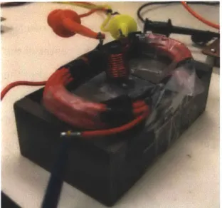
Figure 2-21: Receiver coil (5.6uH) placed at the center of transmitter coil (22uH) ... 38
Figure 2-22: Modified hysteretic tuning controller with PWM... 39
Figure 2-23: Receiver circuit with hysteretic tuning controller (with PWM)... 40
Figure 2-24: Gate voltage of the detuning MOSFET for hysteretic tuning controller with PWM (for 2 different loads)... - -. ---... ---Figure 2-25: Receiver circuit w ith buck converter ... ... 41
Figure 3-1: A typical transmitter circuit (with the receiver coupled)... 42
Figure 3-4: Cross-coupled class-D amplifier (with capacitive divider) - version 2...
Figure 3-5: Voltage on sides 'acn' & 'acp' of the primary LC tank (with version 2) ... 46
Figure 3-6: Current in the primary coil (with version 2 circuit)... 47
Figure 3-7: Actual setup of the cross-coupled class-D amplifier (version 3) ... 47
Figure 3-8: Cross-coupled class-D amplifier with capacitive divider and level shifter (version 3)... 48
Figure 3-9: Voltage on the zener (version 3 circuit)... 49
Figure 3-10: Gate voltage of M1 (blue) & drain voltage of M1 (red) ... 50
Figure 3-11: Gate Voltage of M2 (black) and drain voltage of M2 (purple) ... 50
Figure 3-12: Gate voltage of M1 and M2... 51
Figure 3-13: Change in tank voltage's overlap time by varying Vref ... 52
Figure 3-14: Resistance of a differential cross-coupled NMOS pair... 53
Figure 3-15 : M odifie d Royer ... 54
Figure 3-16: Test setup to investigate the base drive ... 56
Figure 3-17: Royer - board (primary coil not shown) ... 57
Figure 3-18: Royer - voltage across the primary LC tank with no secondary circuit coupled (VDc=10V, Vacprimary = 62Vp.pfo =106kHz) ... 57
Figure 3-19: Collector and Base voltage of left and right transistors in royer (dark blue = base voltage of left NPN, light blue = collector voltage of left NPN, green = collector voltage of right NPN, pink = base vo ltage of right N PN )...58
Figure 4-1: Overall Power Efficiency of the open loop system... 60
Figure 4-2: Direct Feedback from Secondary to Primary ... 61
Figure 4-3: bqTESLA - Resistive Modulation ... 62
Figure 4-4: bqTESLA - Capacitive Modulation... 62
Figure 4-5: Supply Current vs. Supply Voltage when a resistor Ri is connected across a voltage source). 64 Figure 4-6: Supply Current vs Supply Voltage Curve when load Ri is regulated by DC/DC converter... 64
Figure 4-7: Supply Current vs Supply Voltage with dissipative resistor R2 ... .. . .. .. . . .. .. . .. . .. . . . 65
Figure 4-8: Model of Resonant Inductive System (including parasitics) ... 66
Figure 4-9: Primary Supply Current (rms) vs. Primary Supply Voltage (rms)... 67
Figure 4-10: Primary Supply Current vs. Primary Supply Voltage... 68
Figure 5-1: Closed Loop Transmitter Setup ... 70
Figure 5-2: Closed Loop Transmitter with OPTR in more detail... 71
Figure 5-3: Optimal Power Transfer Regulator - Circuit block diagram ... 73
Figure 5-4: Simple Slope Detection Algorithm - initial sweeping... 76
Figure 5-5: Simple Slope Detection Algorithm - dithering ... 76
Figure 5-6: Simple Slope Detection for multiple loads ... 76
Figure 5-7: Overview of State Diagrams ... 78
Figu re 5-8 : C o ntro l SM ... 79
Figure 5-9 : Sw eep/D ither SM ... 80
Figure 5-10: D/A Converter SM ... 81
Figure 5-11: Delay A/D Converter ... 82
Figure 5-12: A/D Converter SM ... 83
Figure 6-1: Closed Loop Transmitter - OPTR and DC/DC Converter... 85
Figure 6-2: Coupling between the Primary and Secondary coils ... 87
Figure 6-3: Overall Power Efficiency vs Secondary Load ... 88
Figure 6-4: Power Output of the Primary vs. Secondary Load...89
Figure A-1: Full schem atic of the test setup ... 92
Figure A -2: Picture of the setup ... 93
Figure C-1: Royer circuit coupled to the Receiver with hysteretic tuning controller circuit ... 120
List of Tables
Table 1: Comparison of power efficiencies with different tuning controllers ... 37Table 2: Effect of Capacitive Divider Ratio... 43
Introduction
Power and signals can be transferred electromagnetically either via direct electrical connections in a closed circuit or wirelessly. Since the early days of electromagnetism, methods to transfer signals wirelessly over large distance have evolved rapidly. However, development of wireless power transmission systems (across large air gaps) is lagging behind the progress in wireless communication even though Nikola Tesla demonstrated as early as 1900s that energy can be transferred wirelessly [1]. This is mostly due to the huge power losses associated with transporting energy over long distances.
Wireless transfer of energy can be achieved by non-radiative methods (near-field) or by radiative methods (far-field) such as omni-directional antennas and lasers. There are several drawbacks in using radiative methods to transfer energy: most of the energy is lost in free space and/or requires direct line of sight with the object. However, with non-radiative modes such as inductive power transfer or capacitive power transfer, radiative losses are reduced because the magnetic field or the electric field is localized.
The basic concept behind inductive power transfer is equivalent to the working of a traditional transformer except for the difference in coupling factor. In a transformer, the primary and secondary coils are tightly coupled with the coupling factor approximately equal to
1. But in an inductive power transfer system, the coupling factors can range from 0.1 to 0.6
depending on the separation between the primary and secondary coils. Resonant inductive coupling, which is inductive coupling with resonance added to the equation, is more suitable for transferring energy in loosely coupled systems [2], [3]. Inductive coupling and resonant inductively coupling are explained in more detail in chapter 1.
One main drawback with inductive coupling is the inability to transfer power through metal objects: when metal objects are placed in a magnetic field, significant amount of power is dissipated due to the formation of eddy currents in these objects. However, in capacitive power transfer this drawback is not present because instead of a distributed magnetic field, a
distributed electric field links the plates of a capacitor which are separated by the air gap [4]. One of the capacitor plates is free and can be used to transfer power to a movable load. However, sufficiently high voltage across the capacitor plates can exceed the electric breakdown voltage of air and cause capacitive power transfer to fail.
With the elimination of cables, wireless energy can make life truly mobile by charging consumer electronics like mobile phones to providing power to movable loads such as motors at the end of a crane. Implementation of wireless energy can also charge medical implants without requiring frequent surgeries to replace batteries. Also, wireless power transfer systems can be scaled to provide a broad range of power levels which support a wide variety of products and systems.
In this thesis, a medium range (5-10 cm) wireless power transfer system that can provide 0.5W to 5W of power is built and tested. The system employs resonant inductive coupling to transfer power. Later in the thesis, the power efficiency of the system is optimized by the implementation of Optimal Power Transfer Regulator which uses indirect feedback from the secondary to ensure that the primary (or the transmitter) provides just enough power to regulate secondary (or receiver) load and minimizes standby power losses [5].
Chapter organization of this thesis is as follows: Chapter 1 discusses inductive and resonant inductive coupling in more details; Chapter 2 and 3 discusses the receiver and transmitter architecture of the open loop system respectively; Chapter 4 discusses the problems with the current open loop setup and introduces a novel indirect feedback method to implement the Optimal Power Transfer Regulator: Chapter 5 discusses the implementation of the Optimal Power Transfer Regulator (OPTR); in Chapter 6 the new closed loop system with OPTR is tested
by evaluating the improvement in the power efficiency in comparison to the previous open
References
[1] N. Tesla, "Apparatus for transmitting electrical energy". New York Patent 1119732, 01 December 1914.
[2] A. Ghahary and B. H. Cho, "Design of transcutaneous energy transmission system using a series resonant converter," IEEE Transactions on Power Electronics, vol. 7, no. 2, pp. 261-269, Apr 1992.
[3] A. Karalis, J. Joannopoulos and M. Soljacic, "Efficient Wireless non-radiative mid-range energy transfer," Annals of Physics, vol. 323, no. 1, pp. 34-48, 2008.
[4] C. Liu and A. P. Hu, "Power flow control of a capacitively coupled contactless power transfer system," in Industrial Electronics, 2009. IECON '09. 35th Annual Conference of IEEE, Porto, 2009.
[5] E. T. Lisuwandi and T. Bogoda, "Primary Unit Control of Resonant Inductive Power Transfer System for Optimum Efficiency". Patent Pending.
Chapter 1
Inductive Power Transfer System
In an Inductive Power Transfer System, energy is transferred across a physical gap between the primary and the secondary by electromagnetic induction. The basic structure and operation of an Inductive Power Transfer system is discussed in this section.
1.1 Inductive Power Transfer
TX coil p riTransmitter Vsupply +Circuit Primary Unit RX coil Receiver Circuit Secondary Unit
Figure 1-1: Typical Inductive Power Transfer System
A typical setup of an Inductive Power Transfer system is shown in figure 1-1. The system consists of a primary unit and a secondary unit which are electrically isolated. The transmitter circuit and transmitter coil are contained in the primary unit. The transmitter circuit, powered by supply voltage (Vsupply), is a DC/AC converter which creates an alternating current in the transmitter inductor loop (TX coil). The secondary unit contains a pick up coil (or receiver [RX]
the receiver coil due to the inductive coupling between the two coils. The A/C voltage induced across the receiver coil serves as the supply voltage to the secondary unit. Inside the secondary unit, the A/C voltage is rectified and fed as the input to the regulator circuitry.
Depending on the distance and the alignment of the receiver coil with respect to the transmitter coil, the receiver coil absorbs only a part of the magnetic flux generated by the transmitter coil. Coupling factor, k, is a measure of the amount of flux generated by the transmitter coil linking the receiver coil. The value of k ranges from 1 to 0: coupling factor of 1 represents that all the flux generated by the primary coil is linking the secondary coil, therefore the two coils are perfectly coupled. A coupling factor of 0 means that none of the flux generated by the primary coil reaches the secondary coil therefore the two coils are not magnetically coupled. In the Inductive Power Transfer Systems considered in this thesis, the coupling factor can range from 0.1-0.6 and therefore are loosely coupled.
In inductive coupling, the energy is transferred due to the coupling of the transmitter and receiver coils. For efficient energy transfer, the receiver coil needs to be tightly coupled to the transmitter coil such that the receiver coil can pick up as much of the magnetic flux generated as is possible. Since magnetic field density weakens with distance, the smaller the separation between the two coils, the stronger their coupling tends to be.
The concept of inductive coupling is similar to the operation of a traditional transformer. However, traditional transformer methods are not generally feasible method to transmit over larger air gaps (for medium range power transmission) [1]. The power transmission range can be improved by using resonance on the secondary unit. Resonance effect can be easily incorporated to the receiver circuit by forming a LC tank on the secondary side. The primary side can also be made resonant by forming a LC tank. The energy coupling is strongest when the primary and secondary LC tanks are tuned to the same resonant frequency and there is weak energy coupling between off-resonant objects. The LC tanks are tuned by adjusting the capacitor and inductor values.
From Coupled Mode Theory [2], it can be shown that resonant inductive coupling delivers more power in comparison to traditional non-resonant inductively coupling when the geometry
and supply voltage is fixed [3]. A more detailed explanation is given using the transformer model in the next section 2.2.
Figure 1-2 shows basic structure of a Resonant Inductive Power Transfer System. The LC tank topology does not necessarily have to be in parallel configuration. The transmitter and receiver circuits are discussed in more detail in chapter 3 and chapter 2 respectively.
0 Regulator
isupply
DC/AC Cnk-t-- Lankt L ank-rx
+Converter Cakix Lan-xCakr lRa
Vsupply--- ~
Primary Unit Secondary Unit
Figure 1-2: Resonant Inductive Power Transfer System
1.2 Resonant Inductive Coupling: Transformer Model
The transformer model shown in figure 1-3 can be used explain the operation of resonant inductively-coupled systems.
L1 is. 1: n
Vsecondary
Vprimary is the independent A/C voltage across the primary LC tank which supplies power to the system. The A/C voltage, Vsecondary, is voltage developed at the secondary side due to the magnetic coupling between transmitter and receiver coils. C, and C, are the capacitors on the primary and secondary side LC tank respectively. The mutual inductance (Lm) between the primary and secondary coils due to magnetic coupling is given by,
Lm = kj1L2
where L1 and L2 are the self-inductances of the primary and secondary respectively. The
self-inductance of the primary (L1) and secondary (L2) are given by,
Lm
L1 = L1 1 + -n or ( L1 = L1 1 + L,)
Lz = L12 + nLm
where,
LIi = leakage inductance of the primary
L,= magnetizing inductance of the primary n = turns ratio
L12 = leakage inductance of the secondary
The secondary side from figure 1-3 can be reflected to the primary resulting in a simple circuit shown in figure 1-4.
ip 's' Lr V p r im a r y - _ _ -IC Li m L Cr
C, is the reflected capacitance of the secondary and Lr is the reflected leakage inductance of the secondary. When the transmitter and receiver coils are loosely coupled, the secondary leakage inductance is significantly larger than the magnetizing inductance. Therefore, in an inductively coupled system if C, is set to 0, most of the primary current ip will flow through the magnetizing inductance (im>>is') and back to the source. However, in resonant inductively coupled systems, the addition of the secondary capacitor lowers the secondary impedance at resonance. Hence, resonant inductive coupling transfers power across larger air gaps much more efficiently [3].
When the transmitter and receiver coils are tightly coupled in a resonant inductive system, mutual inductance, Lm, increases and the secondary leakage inductance, 112, drops. The resonant frequency of the secondary LC tank shifts away from the primary resonant frequency. Therefore, the tightly coupled receiver does not pick up as much energy as the loosely coupled receiver coil. When the receiver coil is tightly coupled, Lr in figure 1-4, drops significantly and reflected secondary impedance is dominated by the reflected secondary LC tank capacitance, Cr. At the primary resonant frequency, secondary impedance is not lowered (unlike in the loosely coupled system). For tightly coupled systems, the traditional non-resonant coupling method transfers power more efficiently. The resonant inductive coupling method is more effective at enhancing energy transfer for lower coupling factors. Hence, when the geometry of the transmitter and receiver coils is fixed, resonant inductively coupling has an optimum coupling factor when the system is not too loosely coupled or too tightly coupled.
1.3 Transmitter and Receiver Coil Magnetics
1.3.1 Quality Factor
(2rf)L R
Depending on the amount of power transfer, the current flowing through the transmitter loop can easily vary over a large range (for example from 1A to 10A in the prototype system described in this thesis). To reduce standby power losses, the series resistance of the transmitter and receiver coils must be minimized.
1.3.2 Optimum Coil Geometry
For the receiver coil to pick up as much magnetic flux as possible and develop that flux in to a large voltage, both the number of loops and the area of each loop need to be large. In one coil configuration, the area of each loop is fixed and the number of loops can be stacked vertically (see figure 1-5). However, loops that are away from the transmitter's magnetic field will pick up smaller amounts of magnetic flux, while still contributing loss. After a certain (optimum)
number of loops, the losses due to the series resistance start to dominate which will reduce the amount of power transfer to the secondary (see figure 1-6).
Maximum Pickup
No. of loops in the coil
Figure 1-6: Maximum pickup vs number of loops
Instead of stacking the loops vertically, the loops can be wound on the same plane so that all the loops pick up the optimum magnetic flux and the area of each loop keeps increasing as loops are added (see figure 1-7). The same coil configuration can be used for the transmitter coil.
Figure 1-7: Transmitter (or Receiver) coil
1.3.3 Addition of Ferrite Material
A ferrite block placed underneath the transmitter loop improves the pickup by the receiver
dramatically. The ferrite block needs to be placed underneath the loop (not in the center of the transmitter coil). When the ferrite block is placed underneath the loop the magnetic field of the current loop is more vertical and concentrated inside the loop. The ferrite block is acting as
'magnetic flux guide' by guiding the magnetic field underneath the loop more into the center of
the loop and strengthening the field inside the loop. Figure 1-8 and 1-9 show the loop without and with the ferrite material respectively.
Figure 1-8: Magnetic field of a single loop Figure 1-9: Magnetic field of a single loop with
with no ferrite material ferrite material
The ferrite block has to fit the size of the loop. If the ferrite block is bigger than the loop
itself, the receiver pickup decreases. The magnetic field in the center of the loop is probably less vertical and uniform. If the ferrite block is placed inside the loop (i.e between the primary and secondary, the ferrite tends to short out the magnetic coupling which makes it harder for the receiver to pick up any magnetic flux. The magnetic flux pattern for a loop with a ferrite
block larger than the size of the coil is shown in figure 1-10.
Figure 1-10: Magnetic field of a single loop with a ferrite block larger than the loop
When more than one loop is used as the transmitter (for example having two loops next to each other) the ferrite block helps to guide the magnetic flux between the loops. Hence, the
effect of having the second loop is more pronounced. The ferrite block helps to direct and strengthen the magnetic field density of a loop at certain locations by placing loops with current flowing in the same or opposite direction in different orientations.
References
[1] Ghahary, Ali, and Bo H. Cho. "Design of a Transcutaneous Energy Transmission System Using
a Series Resonant Converter." IEEE TRANSACTIONS ON POWER ELECTRONICS 7.2 (1992):
261-69. Print.
[2] H.A. Haus, Waves and Fields in Optoelectronics, Prentice-Hall, New Jersey, 1984.
[3] Karalis, A., J. Joannopoulos, and M. Soljacic. "Efficient Wireless Non-radiative Mid-range
Chapter 2
Receiver Architecture
The basic receiver circuit introduced in the previous section is explored in more detail in this chapter. The typical structure of a receiver, as shown in Figure 2-1, consists of a LC tank formed
by receiver coil Lt-rx and capacitor Ct-rx which is tuned to the same resonant frequency as the
primary side LC tank formed by Lt-tx and Ct-tx. The Lt-rx is the inductance of the receiver coil when the transmitter coil is not magnetically coupled to it (and Lt-tx is inductance of the transmitter coil when the receiver coil is not magnetically coupled to it). The output voltage of the LC tank is then rectified and connected to a regulator which can be a step down DC/DC converter or a tuning controller.
Regulator
Vpnmar C-L tt fr tr - m la
Figure 2-1: Basic Receiver Circuit (with transmitter coil coupled)
When the primary (transmitter) circuit is coupled to the secondary (receiver) circuit, the system can represented by the transformer model in Figure 2-2 (the transformer model is
explained in more detail in chapter 1). The complete transformer model can further simplified
by replacing the primary circuit with its Thevenin equivalent when looking back from the
secondary tank capacitor (Ct.x) [1]. The simplified circuit is shown in .
Leq
is , 1: n
Vweonda rV
vpfmi
Vei
Figure 2-2: Complete Transformer Model
Lieq
secandary
Veq
Figure 2-3: Primary Circuit replaced with Thevenin Equivalent
In Error! Reference source not found., Leq is given by,
L12 = leakage inductance of the secondary coil
Lm = mutual inductance between the primary and secondary coil due to magnetic coupling n = number of turns from the primary to the secondary
and Veq is given by,
Veq k Vprimary
where,
L1= self-inductance of the primary (see chapter 1.2) L2 = self-inductance of the secondary (see chapter 1.2) k = coupling factor between the primary and secondary coils
Vprimary = AC voltage applied across the primary LC tank
The receiver circuit in Error! Reference source not found. is modified to take into account the coupling between the transmitter coil and the receiver coil to produce the circuit in Error!
Reference source not found..
[ ... Regulator
Veq ,.ur Co- CO Riosa
2.1 Receiver with Tuning Controller
Various receiver circuits can be designed by changing the LC tank topology (e.g. parallel, series and parallel-series) and adjusting the tuning controller to regulate the output voltage accordingly. The tuning controller uses negative feedback to regulate the output voltage by changing the resonant frequency of the secondary LC tank [2].
2.1.1 Different Topologies
2.1.1.1 Parallel LC Tank - Tuned to Detuned
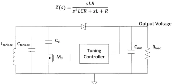
Figure 2-5 shows a receiver circuit with the LC tank in parallel configuration. The impedance, Z, of a parallel RLC circuit is given by,
sLR Z(s) = s2LCR + sL + R Ltank-rx t Voltage Rload
Figure 2-5: Parallel LC Tank Receiver Circuit (with no transmitter coil coupled)
When the tuning controller is switched off (i.e when MOSFET Md is turned off), the secondary LC tank operates at the same resonant frequency as the primary LC tank and absorbs the maximum possible amount of energy from the transmitter coil. When the output voltage exceeds the regulated output level (which is set internally in the tuning controller), the tuning controller turns on the MOSFET Md and adds the capacitor Cd to the secondary LC tank. The resonant frequency of the secondary LC tank is changed to a lower value ('detuned') due to the addition of capacitor Cd. When detuned, the secondary LC tank absorbs less energy from transmitter. The receiver achieves regulation by controlling the amount of energy picked up by the secondary LC tank using the tuning controller. The impedance curves when the secondary
LC tank is in tune with the primary and when detuned are plotted in Figure 2-6.
detuning
E I
Frequency (rad/s)
In Figure 2-6, the green curve is the impedance of the LC tank when the detuning capacitor Cd is switched off. The impedance curve shifts to the left when Cd is switched on (blue curve).
The upper limit of the load regulation range (that is the upper limit of the load current for when the output voltage level is in regulation) is determined by the maximum amount of energy picked by the receiver coil. The lower limit of regulation is set by the value of the detuning capacitor. Ideally, the receiver should be in regulation when the load current is 0 A. This condition requires the detuning capacitor to be replaced by a wire to essentially short the secondary LC tank and prevent the receiver from absorbing any energy from the primary. However, then the detuning switch, Md, must be able to handle a large amount of current to completely detune the secondary LC tank. Therefore, the practical approach to extend the lower limit of regulation is to place a big enough detuning capacitor (in this setup about luF). The value of this detuning capacitor will determine how much the impedance curve in Figure
2-6 will shift to the left and thus the regulation range.
One caveat is presented with this parallel LC tank receiver topology: when the receiver coil is tightly coupled to the transmitter coil, large voltages can be generated in the receiver circuit because the secondary LC tank starts off being in tune with the primary. This problem can be alleviated by setting the LC tank to be detuned in the first place and capacitor added to the network to make it in tune with the primary. An example of such method is shown with a parallel-series LC tank method shown in the next section.
2.1.1.2 Parallel-Series LC Tank - Detuned to Tuned
The parallel-series topology shown in Figure 2-7 is initially detuned and is tuned to the primary resonant frequency when the tuning controller switches on the MOSFET Md. Parallel-series receiver circuit has the tank capacitor, Ct, in Parallel-series with receiver coil, Lt, and the detuning or rather the tuning capacitor, Cd, in parallel with receiver coil. When Md is switched on, the total tank capacitance is Cd+Ct. The resonant frequency (fo) of the parallel-series LC tank shifts
Ct-r Output Voltage
Vprim ar-~E
CI T u n in g _ _C o, u R11,Da
-- ~controller
--Figure 2-7: Parallel Series LC tank receiver (with transmitter coil coupled)
Ct-r- Output Voltage
Ve-Tuning Coki Rrjd
Controller
Figure 2-8: Simplified Parallel Series LC tank receiver
Capacitor, Ct, controls the minimum load required to maintain regulation. Therefore, by
decreasing the value of Ct, the receiver can regulate smaller minimum loads. However, the
same capacitor Ct also controls the amount of power delivered to the load therefore Ct needs to be sufficiently large to power the tuning circuitry and achieve regulation in the first place.
Capacitor, Cd, controls the upper limit in the load regulation range. Bigger value for Cd
increases the maximum amount of load current the receiver circuit can have while maintaining voltage regulation at the output. However, two factors constrict the value of
Cd-1. Since the receiver is shifting from detuned to tuned by adding Cd to the tank, Lt and Ct+Cd combination need to match the primary resonant frequency. Unlike in the parallel
LC tank receiver, Cd cannot be set to an arbitrarily large value: the primary resonant frequency sets a limit on Cd.
2. The amount of power delivered to the load is still controlled by capacitor Ct. In order to increase the upper limit in the current load regulation range, Ct and Cd both must be increased.
Though the parallel series receiver prevents any large voltages build up in the receiver circuit during power up, the load regulation range is severely limited in comparison to the parallel receiver. The ideal receiver configuration, which a combination of both parallel and parallel-series receivers, is shown in Figure 2-9.
Tuning --C I' Controller Output Voltage Ct Cot Rload Lt
Figure 2-9: Parallel Series LC tank (with detuning capacitor across tank capacitor)
The receiver is initially detuned and tuned to the primary LC tank with addition of capacitor Cd- Since detuning/tuning capacitor Cd is added across the Ct, the receiver can regulate higher current loads by delivering more power to the load. However, implementing the gate drive for
MOSFET Md is rather challenging. For this thesis, the parallel LC tank receiver topology was
2.1.2 Switching Techniques for the Tuning Controller
The tuning controller consists of an operational amplifier or a comparator which compares the rectified output voltage to a previously set reference voltage and produces a voltage that controls the gate of the detuning MOSFET. Different tuning controller circuits can be implemented mainly by employing different methods to switch the detuning MOSFET. The two such techniques are discussed in the following section.
2.1.2.1 Switching technique: Linear
The receiver circuit in Figure 2-10 uses a tuning controller which drives the gate of the detuning MOSFET, Md, linearly to regulate the output voltage. The negative feedback is formed as follows. The operational amplifier LT1018 compares the output voltage, which is divided down by the resistor divider set by resistors R3 and R4, to the reference voltage set by the two diodes D2 and D3. The output of the operational amplifier is filtered by the RC low pass filter set by C3 and R1 (f3dB = 72.3 kHz) and drives the gate of the detuning MOSFET Md. The output voltage of this receiver circuit is regulated at about 1OV.
D, Output voltage CMSH1-100M Cd R luF 2k LT1018 10k Lt Ct I 0 11 cout 1k +47uF ] T M, Rload
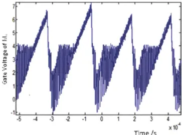
Figure 2-11 shows the gate drive of Md. The gate voltage switches linearly but is not driven all the way to the output voltage. The negative feedback loop is unstable therefore the gate voltage, as seen in Figure 2-11, is oscillating. Some higher frequency components observed on the gate waveform are attributed to the oscillating waveform at resonant frequency coupled from the drain of Md to the gate. Other high frequency content is due to the parasitic inductances present on the circuit board.
Z M1 koI X 4 x10 Time /s
Figure 2-11: Gate voltage of the detuning MOSFET
Linear switching is not the optimum method to drive detuning MOSFET: a significant amount of power is dissipated in the MOSFET Md.
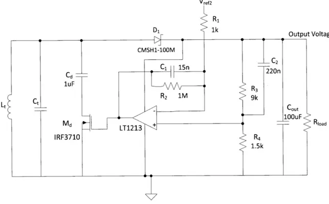
The tuning controller in Figure 2-13 stabilizes the gate voltage of Md. Vref2 was set to about 1.3-1.4V. This approach is even more inefficient at driving the gate of
Md-Vref2 R1 1k Output Voltage CMSH1-100M C2 C1 15n 220n luF R3 R2 1M 9k 1OOuF
T
Md +.~ +-- RlaFigure 2-13: Tuning controller with stabilized linear switching
43[ 1 -4-J 0. 42 0.01 0 M Time /s
Figure 2-14: Gate voltage of detuning MOSFET (stablized linear switching)
During certain points of operation the circuit briefly becomes unstable. This observation can probably be explained by the gain curve. The gain curve is a graph of gate voltage of Md (Vg) plotted against output voltage (Vout) when the circuit is driven in open loop. The transfer function is given by,
__= Gm Rioad
1
g Rs + Rload' 1 + s. Cout. Rload
where Rs (source impedance) was measured to be 16.80, Cout is the output capacitor and Gm is simply a constant (refer to circuit in Figure 2-13). As explained previously, the gain curves were plotted by setting Rload to a fixed value and driving the circuit open loop by applying a DC voltage at the gate of Md. Therefore, the slope of gain curve is simplified to,
Rioad
slope = Gm R Rad
Rs + Rioaa
Gain plots for two different loads are plotted in Figure 2-15 and Figure 2-16. The circuit became unstable probably due to the non-linear regions of the gain curves.
Gate Voltage vs Output Voltage for Rioad= 160 Ohms
2.4 2.6 2.8 3 12 14 3.6
Vgate / V
Figure 2-15: Gain curve
Gate Voltage vs Output Voltage for Rjoad = 17 Ohms
1 2.6 28 3 12 14
Vgate / V
Figure 2-16: Gain Curve 0
Power efficiency of the receiver can be increased by improving the gate drive of the detuning MOSFET using hysteresis. The hysteresis switching method is discussed in next section.
2.1.2.2 Improved Switching Technique: Hysteresis
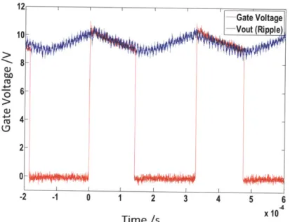
In this switching mode, the gate of the detuning MOSFET is switched harder by driving Md
all the way to the output voltage using hysteresis. Hence, the gate is either on or completely off as seen in Figure 2-17. Some ripple is introduced at the output voltage due to hysteresis (see Figure 2-18). The receiver circuit with hysteresis switching is shown in Figure 2-19.
12 10- 8- 6-0 2-2 -2 -1 0 1 2 3 4 5 6 x10 Time /s
0 4., 0 -2 -1 0 1 2 3 4 5 6 -4 Time /s
Figure 2-18: Output ripple and the gate voltage superimposed
The comparator LTC1440 has programmable hysteresis and a built-in reference which was used to set Vref.
D1 Voltage
Rload
Figure 2-19: Tuning controller with hysteretic switching
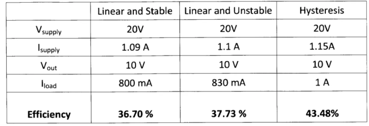
The overall power efficiency was measured for the three switching techniques. The test setup is shown in Figure 2-20. Class-D power amplifier (see Chapter 3 for more details) was
used as the DC/AC converter to generate an AC voltage of 140Vpk-pk across the primary LC tank. The resonant frequency of the primary LC tank was 108 kHz. The DC supply (VSUPPly) to
DC/AC converter was fixed at 20V. The output voltage of the receiver (Vout) was regulated at
1OV.
The receiver coil position was fixed with respect to the transmitter (see Figure 2-21). Themeasurements were taken for the three different tuning controllers. The results are shown in table 1. Output Voltage -- (Vout) Vprmary ( 140V" |||| || Rjoad
Figure 2-20: The test setup to compare power efficiencies of different tuning controllers
Table 1: Comparison of power efficiencies with different tuning controllers
Linear and Stable Linear and Unstable Hysteresis
Vsuppiy 20V 20V 20V
isupply 1.09 A 1.1 A 1.15A
Vout 10 V 10 V 10 V
'load 800 mA 830 mA 1 A
Efficiency 36.70 % 37.73 % 43.48%
There is a significant improvement in overall power efficiency by driving the gate of detuning MOSFET with hysteresis. However, the switching of detuning capacitors is more audible with the hysteresis gate drive. The tuning controller implemented in Figure 2-22 uses pulse width modulation to fix the switching frequency of the tuning capacitor at (non-audible) frequency of 30 kHz. D1 Output Voltage Vout CMSH1-100M Cd luF R3 Lt C MI k C o -Ri 47uF Md -- - ~ Rload
Figure 2-23: Receiver circuit with hysteretic tuning controller (with PWM) ThkStop I -MMr 2.OOV NI1O.O;s! A4 Ch2 X Oo.OO I 2.23 V lhStop ME 2.00 V M1O.OJLSI A Ch2 r 2.2SV 1ls0.00 a
Figure 2-24: Gate voltage of the detuning MOSFET for hysteretic tuning controller with PWM (for 2 different loads)
___I.
-Tikk ,VO I t
I---
----
---2.2
Future work: Receiver with Buck Converter
The receiver setup in Figure 2-25 replaces the tuning controller with a buck converter to step down secondary LC tank voltage and regulate the output voltage. This receiver configuration is much more power efficient due several reasons.
1. Buck converters can be designed to have high power efficiencies which in turn improves
the overall power efficiency of the secondary unit.
2. A significant amount of power is dissipated in the ESR of the detuning capacitor and the detuning MOSFET during switching. Using a buck converter that can withstand a high voltage input will not require any detuning circuit to pre-regulate the output of the receiver's rectifier.
Figure 2-25: Receiver circuit with buck converter
References
[1] Ghahary, Ali, and Bo H. Cho. "Design of a Transcutaneous Energy Transmission System Using
a Series Resonant Converter." IEEE TRANSACTIONS ON POWER ELECTRONICS 7.2 (1992):
261-69.
[2] Boys, J. T., Covic, G. A. and Green, A. W,: "Stability and control of inductively coupled power transfer systems," IEEE Proceedings on Electric Power Application, Vol.147, No.1, pp37-43, January 2000.
Chapter 3
Transmitter Architecture
The transmitter circuit, which comprises of a DC/AC converter, produces the AC voltage across the primary LC tank to generate a magnetic field. Figure 3-1 shows a typical setup for a transmitter circuit with the receiver (secondary) circuit coupled. The power converter does not necessarily have to be DC/AC converter: it can be AC/AC or AC/DC/AC converter. For this thesis,
DC/AC converter is used for power conversion.
II Il || || Il vsupply Primary Unit Secondary Unit
Figure 3-1: A typical transmitter circuit (with the receiver coupled)
In this chapter, two different topologies of DC/AC converters for a Resonant Inductive
Power Transfer system are discussed.
3.1 Cross-coupled Current Mode Class-D Power Amplifier
The gate drive of a current mode class-D power amplifier can be modified to design a resonant oscillator which then can be used as a DC/AC converter in the transmitter circuit. An
transistors M1 and M2, which control the two current sources, are driven 1800 out-of-phase
[1]. Ideally, the transistors have zero voltage across at the time of switching caused by the resonance filter (formed by the parallel LC tank - Ltank-tx and Ctank-tx). Therefore, the ideal
operation achieves zero-voltage-switching (ZVS). The circuit to the left in Figure 3-2 replaces the two current sources with two large inductors Lsi and Ls2. Lsi and Ls2 are wound on the same core
therefore are tightly coupled. It is important to note where the polarities of Lsi and Ls2 are when
connected in the circuit: this is to ensure that the transistors are driven 1800 out-of-phase. Also the output capacitances of the two transistors become a part of the parallel LC tank.
Ltank-tx Lakt
GaeDiv ae rv M 2 L ate rive
Figure 3-2: A Simplified Current Mode Class-D amplifier circuit
The gate drives of the two transistors M1 and M2 can be cross-coupled (i.e. gate of M1 can be connected to the drain of M2 and vice versa) to design a resonant oscillator. The frequency of such an oscillator will be set by the resonant frequency of the parallel LC tank. In a resonant
inductive power transfer system, Ltank-tx will be the inductance of the transmitter (primary) coil.
Depending on the amount of power delivered by the primary circuit, the voltage across the primary LC tank can be large. Therefore in a practical circuit, the gates of the transistors cannot be directly cross-coupled to the respective drains of the transistors. The drain voltage is divided down before driving the gate of the transistor. In the next section, implementation of the gate drive is discussed in more detail.
3.1.1 Gate Drive
Three different versions of gate drive implementations were tested. The first version of the gate drive implemented with a resistor and zener is shown in Figure 3-3. This is an inefficient way to drive the two MOSFETs because a significant amount of power dissipated in the 1kQ
resistors and two zeners. The output waveform across the LC tank is distorted and becomes even more distorted when the supply voltage is increased. This transmitter cannot operate at
higher voltages (more than 1OV) as the resistor and zener gets too hot to function.
M1 M2
Figure 3-3: Cross-coupled class-D amplifier (with zener and resistor) - version 1
In the second version, the resistor and zener was replaced with a capacitive divider (Figure 3-4). The output of the capacitor divider is then sent to a comparator (followed by an inverter) to drive the gate of the MOSFET harder to minimize power dissipation in the MOSFETs. In this
To find the optimum operating point for the transmitter, different ratios for the capacitor divider were tested (Table 2). The ratio of the capacitive divider is given by the following expression, C2 C1 C2 + C3 C1 + C4 Vqupply L1 L2 2m CS 2m W L3 C CI~ C1 C2 100n 10 n M16 WIfif M2 IRF3710r U2' C- _
---Figure 3-4: Cross-coupled class-D amplifier (with capacitive divider) - version 2
Table 2: Effect of Capacitive Divider ratio
Ratio C1,C2 C3,C4 Max. primary Max. Tank Voltage Max. Supply Max. Supply
loop current (Vacp - Vacp)/Vp.p Voltage Current /A
IlfAp.p VSUPPIY /V 0.68 47n 22n 3.7 55.6 9.5 0.7 0.5 47n 47n 4.1 59.6 10 0.8 0.5 100n 100n 3.1 46.8 8.6 0.9 0.4 100n 150n 4.1 52.8 9 0.9 0.32 47n 100n 5.37 78.4 13.5 0.8 0.24 47n 150n 6.8 111 20 0.8 0.24 68n 220n 7.2 113 20 0.7 0.23 100n 330n 7.7 115 20 0.56
Table 2 shows the maximum current through the primary coil and LC tank voltage that can be reached without heating up the capacitor divider and the zener too much for different capacitor ratios. For higher ratios, the maximum supply voltage that can be reached is about 1OV. At higher ratios, the voltage across the zener is clipping therefore power is dissipated in both the zener and ESR of the capacitors. At a ratio of 0.24, the capacitor divider and the zener were getting hot but comparatively less to the original setup in Figure 3-3.
I ~~ ~ L - aCD ..- acn 40 - 30-Voltage/v 10 - -0 -10 Time/ s
Figure 3-5: Voltage on sides 'acn' & 'acp' of the primary LC tank (with version 2)
Note: Frequency of the waveforms is approximately 230 kHz
Figure 3-5 shows the voltage at ACP and ACN nodes of the transmitter. The voltage across the LC tank would be ACN - ACP. The voltage output across the tank is not sinusoidal. The
overlap between two waveforms can be minimized by bringing down the reference voltage,
Vref, to about OV on the LT1720 comparator.
3-
2-Current A /
Time uS
Figure 3-6: Current in the primary coil (with version 2 circuit)
This circuit has a startup issue. Reference voltage, Vref, on the comparator can be set to zero during operation but when circuit is starting up, Vref need to be at a higher value (about 3V) and then slowly decreased to OV. This is to ensure that one of the MOSFETs switches to deliver power to the LC tank. If Vref is set to zero at startup, the supply gets shorted as both MOSFETs (M1 and M2) turns on caused by the initial rising edge on ACP and CAN when the supply is first turned on. In the third version of the cross-coupled class-D amplifier, the startup issue is solved
by an RC network to slowly bring Vref from 5V (Vcc) to 0V with a slow time constant (see figure
10). In the third version of transmitter, the gate drive is further improved by adding a level shifter to drive the gates of M1 and M2 harder. In the third version, all passive components are
replaced by the surface mount typess to reduce energy dissipated due to ESR (see Figure 3-7).
R4 100 BSS84 M5 M1 BSS123 Ve1. Vauppey
Figure 3-8 shows the full schematic for the version 3 of cross-coupled amplifier. The LC tank values are C5=47nF and L3=22uH. The capacitor (47nF) in the LC tank is made up by ten of 4.7nF in parallel to distribute the heat dissipated more efficiently. Supply voltage to comparator, Vcc, is 5V. Supply voltage to the level shifter, Vcc2, can be 5V or greater (up to Vgsmax of IRF3710 which is 20V) However, the MOSFETs (Si3552) used in the inverter, which drive the gates of M1 and M2, can handle only up to 2A. Therefore the maximum value we set Vec2 is about 7-10V. The ratio of the capacitor divider is reduced to 0.043. The voltage across the zener
is not clipping anymore (see Figure 3-9 ) therefore it is not getting heated up.
2.52 -1.5 Voltage / V 1 0.5 . 0 -0.5 Time / us
Figure 3-9: Voltage on the zener (version 3 circuit)
The capacitors C15 and C16 (in Figure 3-7) eliminate the ringing on the output waveform. The ringing was probably caused by inductance from the leads of the two MOSFETs M1 and M2. Note however that C15 and C16 are now part of the LC tank. Therefore, the effective capacitance of the LC tank is Ceff = C5 + 0.5(0.luF) = 97nF. The resonant frequency of the transmitter is 108 kHz.
Figure 3-10 shows the voltage at node 'ACN' (red) and gate voltage of M1 (blue). Similarly, Figure 3-11 shows the voltage at node 'ACP' (purple) and the gate voltage of M2 (black). In both
ACP and ACN waveforms the falling edge is slower compared to the rising edge. At the end of
current source (refer to Figure 3-2). This can be seen in figure 3-12 where both gate voltages are plotted on the same graph.
70 -80 50-40 - Gate Voltage ACN / V of M1 /V -12 -1 -0a -0o -04 -02 , Time / xlOuS x 10
Figure 3-10: Gate voltage of M1 (blue) & drain voltage of M1 (red)
ACP / V Gate Voltageof M2
Gate Voltage / V 3
Figure 3-12: Gate voltage of M1 and M2
(The gate voltage of M2 has some ringing on the rising edge of the waveform. This is due to parasitic inductance on the path connecting the inverter to the gate of M2.)
The time during which both MOSFETs are switched off can be reduced by decreasing the reference voltage of the comparator, Vref, to a negative value (about -0.2 to -0.3 V) which switches on the MOSFET a little early. Another solution would be to increase the ground nodes of the zeners to a more positive voltage (about 0.2-0.4V). By reducing the two MOSFETs switching off time, the overlap between the two waveforms ACP and ACN can be reduced (see Figure 3-13).
The caveat with this transmitter board is that the supply voltage to the comparator (Vcc) needs to switched on after switching on the Vsupply. VSUPPIY needs to be greater than about 12V for the transmitter to work due to the smaller capacitor divider ratio.
The startup issue is not completely resolved even in the third version of the cross-coupled class-d amplifier with the RC network to bring Vref slowly down from 3V to 0. Startup requirements for this circuit are discussed in the next section.
Vref = -0.2 V Cu 4-'0 aJ CU 1 1.2 1.4 1.6 1.8 Time /s x105 1 1.2 1.4 1.6 1.8 Time /s x1075 Cu 1 Time / s 1.4 bD 1.6 x 10 1.2 1.4 Time /s 1.6 x
10-Figure 3-13: Change in tank voltage's overlap time by varying Vref
3.1.1 Startup Requirements of the Cross-coupled Class-D amplifier
For cross-coupled class-D oscillator to start oscillating, minimum amount of loop gain or similarly minimum amount of negative resistance is required [2]. To evaluate the startup conditions of the circuit, transconductance is set to its small signal value because the circuit operates in the small signal region before the oscillations have built up in the circuit [3].
Figure 3-14 shows the resistance Ra looking in to the differential cross-coupled NMOS pair. Let RT be the equivalent parallel resistance of the primary LC tank that is in parallel with Ra. gm is
0
Ra
Figure 3-14: Resistance of a differential cross-coupled NMOS pair
From small signal analysis of the differential cross-coupled NMOS pair, Ra is given by, 2
Ra
--Parallel equivalent resistance of the LC tank, RT, is a positive value therefore for the overall
resistance to be negative,
1 1
-+- < 0
Ra RT
After simplifying the above expression to ensure the cross-coupled class-D oscillator to
start,
2
9m >
-RT
When the secondary (receiver) circuit is not coupled to the primary circuit, RT is the parasitic
parallel resistance of the LC tank. When the secondary circuit is coupled to the primary, the
secondary load is reflected to the primary and will be included in RT in addition to the parasitic resistance of the LC tank. The startup of the oscillator is sensitive to the secondary load conditions and the parasitics of the LC tank. Therefore, the startup of the oscillator is not guaranteed. The cross-coupled class-D amplifier is not a practical solution for resonant inductive power transfer systems. In the next section, Royer oscillator is introduced and
3.2 Royer Oscillator
Modified version of the original royer circuit is shown in Figure 3-15 [4],[5]. The original royer circuit used the saturation of the transformer to define the switching frequency which produced a square wave output. In the modified royer, the switching occurs due to the saturation of the transistors. The switching frequency is set by the LC tank formed by Ct-tx and Lt-tx which is the primary LC tank. Lt-tx is the inductance of the primary (or transmitter) coil. The
resonant frequency circuit in Figure 3-15 is set about 103kHz. Unlike the original royer, the circuit is forced to run sinusoidally by the LC tank.
1: 1: 0.02
I
Ls] L 50kO FZT849 1mH LbThe startup in royer is guaranteed: when the DC supply, VDC, is switched on, the transistor
on the left (Figure 3-15) is biased which ensure self-starting of oscillations. The switching occurs
when the on (left) transistor comes out of saturation and the spike in collector current is picked up by the base windings (Lb) and switches on the right transistor.
The voltage across the primary LC tank is given by,
Vacprimary = 2TUVDC (peak-to-peak)
The maximum supply voltage, VDC, which can be applied is limited by the base to emitter reverse breakdown of the NPN which is typically around -6V. The maximum reverse voltage is
given by,
Lb
Vreverse, max = O.5WVDc
-By adjusting the turn ratio between the transformer's primary winding (Ls1) and the base winding (Lb), the maximum supply voltage can be increased.
3.2.1 Base Drive
The base drive of the royer in Figure 3-15 is adjusted by varying the base potentiometer.
Using the test setup shown in Figure 3-16, the effect of base drive on the overall power efficiency, incremental power efficiency and maximum secondary load current was tested when
the secondary output voltage was regulated at 8.1V. The supply voltage to royer was fixed at
20V.
Table 3: Effect of Base Drive on Power Efficiency and Maximum Secondary Load
Base Supply Current of royer Maximum Supply Current of Incremental Overall Resistor with no secondary load Secondary royer at max. Efficiency Efficiency
Rb/Q coupled Load secondary load % %
ISTBY/mA load,max/mA Is/mA
575 383 943 986 63.34 38.73
1.07k 343 923 935 63.14 39.98
2.48k 320 908 902 63.19 40.77
5k 310 890 878 63.46 41.05