HAL Id: hal-02136008
https://hal.univ-brest.fr/hal-02136008
Submitted on 21 May 2019
HAL is a multi-disciplinary open access
archive for the deposit and dissemination of
sci-entific research documents, whether they are
pub-lished or not. The documents may come from
teaching and research institutions in France or
abroad, or from public or private research centers.
L’archive ouverte pluridisciplinaire HAL, est
destinée au dépôt et à la diffusion de documents
scientifiques de niveau recherche, publiés ou non,
émanant des établissements d’enseignement et de
recherche français ou étrangers, des laboratoires
publics ou privés.
Compact Analog All-Pass Phase-Shifter in 65-nm CMOS
for 24/28 GHz on-Chip-and in-Package Phased-Array
Antenna
Marcos Lajovic Carneiro, Marc Le Roy, André Pérennec, Raafat Lababidi,
Philippe Ferrari, Vincent Puyal
To cite this version:
Marcos Lajovic Carneiro, Marc Le Roy, André Pérennec, Raafat Lababidi, Philippe Ferrari, et al..
Compact Analog All-Pass Phase-Shifter in 65-nm CMOS for 24/28 GHz on-Chip-and in-Package
Phased-Array Antenna. 23rd IEEE Workshop on Signal and Power Integrity, Jun 2019, Chambery,
France. �hal-02136008�
Compact Analog All-Pass Phase-Shifter
in 65-nm CMOS for 24/28 GHz
on-Chip- and in-Package Phased-Array Antenna
Marcos L. Carneiro1, Marc Le Roy1, André Pérennec1, Raafat Lababidi2, Philippe Ferrari3, Vincent Puyal4, 5 1Univ Brest, 2ENSTA Bretagne, Lab-STICC, UMR 6285, CNRS, F-29200 Brest, France
3University of Grenoble Alpes, TIMA Laboratory, F-38000 Grenoble, France 4University of Grenoble Alpes, F-38000 Grenoble,
5CEA, LETI, MINATEC Campus, F-38054 Grenoble, France
Marc.LeRoy@univ-brest.fr ORCID 0000-0003-0458-0295
Abstract— This paper describes the synthesis method and
implementation in 65-nm CMOS technology of a compact analog phase-shifter (PS) dedicated to 24/28 GHz applications. This PS delivers a phase shift continuously tunable from 0 to 55° and is particularly suited for on-chip or in-package phased-array antenna. The proposed topology, which is based on an all-pass circuit that includes coupled microstrip lines and varactors as tunable components is intrinsically compact and shows an interesting phase-range vs capacitance-variation ratio.
Keywords— Phase shifter; Analog phase shifter; 65-nm CMOS; Phased-array antenna; On-Chip antenn; In-Package antenna
I. INTRODUCTION
In order to achieve even higher data rates while ensuring a continuous growth of the number of connected devices (smartphones, IoT, …), the future wireless networks, e.g. 5G, will use new frequency bands beyond 6 GHz. For example, in the United States, FCC [1] has allocated frequency bands mostly between 24 GHz and 60 GHz. But, 5G mm-wave-channels have been characterized and qualified as unfavourable, which has compelled researchers to develop specifically designed antenna arrays with highly directional and reconfigurable beams in order to balance the link-budget between transmitters and receivers [2]. Several teams have already developed - or are still developing - MIMO or antenna array modules with big efforts on integration and size reduction. The compactness issue is particularly problematic while mm-wave low frequency bands (i.e. at 24/28 GHz) are under consideration. In this paper, the design of an ultra-compact 45° analog phase shifter integrated in 65-nm CMOS technology is proposed to solve the compactness issue. Conventionally, distributed elements (transmission lines) are used beyond 60 GHz in integrated technologies, but here an inherently compact coupled line phase-shifter topology allows such a distributed approach to be relevant at 24 GHz. Moreover, analog phase shifter with continuously tunable phase states is relevant for several reasons: i) if required, it can easily be turn into switched/digital phase shifter, ii) many
applications require a complementary last-level phase-shifter stage to precisely compensate for antenna array impairments or adjust post-correction phase weight, iii) massive MIMO antenna modules rely in theory on a dedicated RF chain per antenna element, which is not suitable for practical large arrays, then, hybrid beam-formers that include both analog and digital phase shifters are under investigation to provide a more realistic trade-off between performance, power consumption and cost.
The paper is organized as follows: after detailing the phase-shifter architecture principle, the essential synthesis equations are provided. Then, the main design steps towards its integration in 65-nm CMOS process are described. Finally, the simulated and experimental results are presented and a discussion is provided.
II. PHASE SHIFTER PRINCIPLE
The proposed analog Phase Shifter (PS) (Fig. 1) can be either considered i) as a Schiffman PS [3] combined with an all-pass lumped topology in order to introduce tunability through varactors, or ii) as a Hayashi all-pass PS [4] where the transmission lines are coupled to improve the phase shift variation thanks to this more freedom degree. A previous study [5]-[6] has validated this approach of Coupled-Lines All-Pass (CLAP) PS and has shown that choosing the coupled-lines length, , at approximately /8 (instead of /4 in [3]-[4]) provides a wide phase variation for a given / varactor capacitance ratio while being matched over a wide bandwidth. Hence, in [5]-[6], about 200° of phase shift variation was demonstrated from for a single cell for / = 10, which is about twice the phase variation obtained by Hayashi’s PS and RTPS (Reflection Type Phase Shifter) in CMOS technologies. Of course, by operating at /8, the area size is theoretically reduced by 50% compared to Hayashi’s PS [4] or RTPS with hybrid coupler. This size reduction also contributes to mitigate insertion loss for identical varactors and thus to maximize the figure of merit (FoM) defined as the ratio between the maximum phase shift and the maximum insertion loss.
Here, the CLAP PS design focuses on a band that encompasses 5G lower mm-wave bands from 24.25 to 28.35 GHz. By using classical even- and odd-modes analysis for the proposed PS (Fig. 1), S21 phase is expressed as
follows [7]: 0 0 1 0 2 2 21 2 1 2 0 0 0 0 2 0 0 2 1 0 0 0 0 2 2 2 2 − − + = − + + − − − o e e o e o e o e o e o Z tan Z cot Z tan tan C C Z Z Z Z tan .C Z Z C C Z Z Z Z θ θ π φ θ ω θ ω ω ω (1)
where and are the even- and odd-modes characteristic impedances of the PS, is the port reference impedance (i.e. 50 Ω), is the electrical length of the coupled line, and , are the capacitance of the varactors, respectively. S11 general
expression cannot be easily simplified excepted for quarter-wavelength coupled lines (= 90° at the working frequency ):
( )
0 2 2 0 0(
2 1 0)
11 0 2 2 2 2 0 2 0 0 1 0 0 1 2 0 4 4 2 1 e e e Z C Z C S f Z C Z C j Z C C ω ω ω ω ω − = + + − (2) Then, the PS can be perfectly matched for the following ratio between the varactor capacitances:2 0 2 1 0 4 = e Z C C Z (3)
Synthesis equations (2)-(3) at / 4 are only applied to provide the initial level of the PS synthesis to be used in the design and optimisation process. For the most interesting integer capacitance-ratio, / = 2, the PS inputs are matched for
0e= 2 0
Z .Z .
In 65-nm CMOS, the varactor capacitance ratio / is restricted in practice to approximately 2 when the highest -factor is targeted. The goal herein is a continuously tunable phase shift of 45° at least with an error of ±5° and loss variation below ±0.5 dB over the whole bandwidth. The characteristic parameters obtained after a first step of design in schematic circuit software are given in Fig.1.
Varactors Coupled
lines
C1min=50fF = 92 Ω C2min=100 fF = 47 Ω C2/C1 = 2 Electric length = 45° at 28 GHz / = 2
Fig. 1. Schematic of the CLAP PS and optimized design values at circuit level.
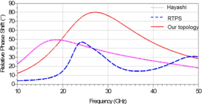
Fig. 2. Phase shift variations for CLAP-PS, RTPS and Hayashi’s all-pass PS from schematic simulations.
To illustrate the interest of CLAP PS to be implemented in CMOS technology with rather small varactor capacitance variation, a comparison of raw configurations of CLAP-PS with Fig. 1 characteristics, and RTPS (with a four-port hybrid coupler and two loads with single varactor) and Hayashi’s PS is put forward under an identical initial set: i.e. same ratio of varactor capacitance, / = 2, and for a working frequency at 28 GHz.
Simulation results are given in Fig. 2. The CLAP PS exhibits a maximum phase variation of 80°, which is almost twice the value from the two other analog PS. Moreover, the circuits are matched from 24 to 30.5 GHz for RTPS, from DC to 35 GHz for Hayashi’s PS and from DC to 70 GHz for CLAP PS, respectively. Hence, under these basic configurations, the CLAP PS exhibits a much wider bandwidth.
III. 65-nm CMOSPSDESIGN,SIMULATIONS AND
MEASUREMENTS
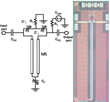
The schematic depicted in Fig. 3 corresponds to the actual CMOS implementation with two varactors in series to get . This allows both a simplification of the biasing network – a single biasing voltage is required – and also C’1 and C2 can
be chosen among available varactors with equivalent variation of their quality factor, Q (cpo12nw in 65-nm CMOS Design Kit (DK) from STMicroelectronics).
The circuit was optimized using ADS, HFSS and Cadence simulation softwares. The main design steps consisted in: i) an optimization in ADS of ideal coupled lines associated with varactors having variable quality factors extracted from the DK (Design Kit), ii) a new round of optimization of the varactor values among the available possibilities of the DK was run while taking into account the S4P parameters of the coupled microstrip lines obtained from HFSS.
For more reliable results, a specific model of the stacked layers was developed in HFSS that allows the optimization of coupled-line widths and slot to fit with the intended even- and odd-modes characteristic impedances.
Fig. 3. Simplified schematic of PS implementation and IC photograph. TABLEI
FINAL OPTIMIZED AND IMPLEMENTED VALUES AND SUMMARY OF SIMULATED RESULTS Parameters Values Line dimensions W = 11 L = 1247 μm, S = 14 μm, μm (electrical length of 75° at 28 GHz) Impedances Z0e = 48.5 Ω, Z0e = 43.1 Ω Varactors C’1 from 76.6 fF to 153.6 fF with Q=22.4 to 14.3 C2 from 145.3 fF to 302.4 fF
Simulation results from 24 to 30 GHz
Phase Max phase variation = 47.8° Max phase error ±2.6°
Insertion loss 2.9dB ± 0.45 dB
Input and output
mismatch |S11|dB and |S22|dB < -11.4 dB
The coupled microstrip lines were designed on Alucap metal layer (made of aluminium), which is the thicker metallic layer on 65-nm CMOS technology, to minimize metallic lossses while the bottom layers M1-M2 were used for the ground. The main features of the final optimized PS are described in Table I together with a summary of the performance obtained in simulation.
The total size of the chip area is of 0.98 mm2 including
testing pads, whereas the core size only features 0.28 mm2.
PS characteristics indicated in Table I differs from the initial synthesis values due to the optimisation goals that mainly focus on phase and insertion-loss flatness over the considered bandwidth.
The measurements were performed for a DC bias sweep ranging from -1.9V to 1.5V as depicted in Fig. 4. The measured results shows a continuous phase shift up to 55° with a maximum phase deviation particularly small of ±0.64°
(reduced below ±0. 4° in the range from 0 to 45°); an input and output return loss better than 13.6 dB, and an insertion loss of 4.3dB ±0.7dB (3.9dB ±0.3dB in 0-45° range). First, it should be pointed out that measured and simulated results are in good agreement. The phase flatness is even better in measurements than in simulation. The varactor quality factor seems to have been overestimated in simulation as evidenced by measured insertion loss with about 1 dB in excess from expectation.
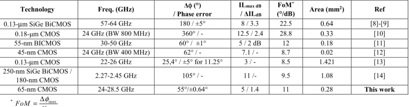
A comparison of previously published integrated analog PS is proposed in Table II. A raw analysis of Table II indicates that the obtained figure of merit is among the state-of-the-art values of analog phase shifter with the smallest phase and insertion loss errors. However, RTPS [8]-[11] provides the higher FoM and a wider phase shift variation but only by using more varactors and for a higher complexity level. Moreover, as illustrated in [11] and by our proposal, increasing the bandwidth and reducing phase and insertion-loss errors will inevitably result in degrading the maximum phase variation and thus the FoM.
Fig. 4. Measured relative phase shift (a), and S-parameters (b).
25.0 26.0 27.0 28.0 24.0 28.5 5 10 15 20 25 30 35 40 45 50 55 0 60 R el ativ e P ha se S hif t (° ) Vbias (a) Frequency GHz) 25.0 26.0 27.0 28.0 24.0 28.5 -12 -10 -8 -6 -4 -2 -14 0 -25 -20 -15 -10 -5 -30 0
(b)
S
21(d
B)
11S
(d
B)
Frequency GHz)TABLEII
COMPARISON OF INTEGRATED ANALOG PHASE-SHIFTERS
Technology Freq. (GHz) Δφ (°) / Phase error ILmax dB / ΔILdB FoM* (°/dB) Area (mm2) Ref 0.13-μm SiGe BiCMOS 57-64 GHz 180 / ±5° 8 / 3.3 22.5 0.64 [8]-[9] 0.18-μm CMOS 24 GHz (BW 800 MHz) 360° / - 12.5 / 2.4 28.8 0.33 [10] 55-nm BICMOS 30-50 GHz 60° / ±1° 5 / 2 dB 12 0.18 [11] 45-nm CMOS 24 GHz (BW 400 MHz) 62° / - 7.1 / - 8.7 0.02 [12] 0.13-μm CMOS 22-26 GHz 25,4° / ±5° for 11.25° 3 / - 8.5 1.421 [13] 250-nm SiGe BiCMOS / 180-nm CMOS 2.27-2.45 GHz 105° / - 11 /- 9.5 1.08 [14]
65-nm CMOS 24-28.5 GHz 55°/±0.64° 5 / 1.4 11 0.28 This work
* max max FoM IL φ Δ = IV. CONCLUSION
In this paper, a 24/28 GHz Coupled-Lines all-pass network was designed and implemented in 65-nm CMOS technology. It has demonstrated an interesting trade-off between relative phase-shift variation for a small / varactor capacitance ratio, phase and insertion loss flatness. Indeed, the PS achieves a 55° continuously tunable phase shift with a phase variation smaller than ±0.64° and insertion loss variation below ±0.7 dB over the tuning range and for the whole considered bandwidth.
The layout is intrinsically compact and could be further shrinked by using meandering microstrip coupled lines or by designing the coupled section on slow-wave coupled CPW lines [11]. Using switched capacitance networks with high quality factor can also be promising in association with this PS topology.
ACKNOWLEDGMENT
This work was supported by the Conseil Départemental du
Finistère (CD29).
REFERENCES
[1] A. Ghosh, « The 5G mmWave Radio Revolution », Microw. J., pp. 22-36, sept. 2016.
[2] C. Bencivenni, T. Emanuelsson, M. Gustafsson, « Gapwaves Platform Integrates 5G mmWave Arrays ». Available on line:
http://www.microwavejournal.com/articles/31753-gapwaves-platform-integrates-5g-mmwave-arrays, 2019-02-08, Microwave Journal [3] B. M. Schiffman, « A new class of broad-band microwave 90-degree
phase shifter”, IRE Trans. MTT, pp. 232-237, avril 1958.
[4] H. Hayashi, T. Nakagawa, K. Araki « Miniaturized MMIC analog phase shifter using two quarter-wavelength transmission lines », IEEE T-MTT, vol. 50, pp. 150-154, 2002.
[5] K. Khoder, M. Le Roy, R. Lababidi, A. Pérennec, « Déphaseur 360° compact large-bande », JNM, Bordeaux, juin 2015.
[6] K. Khoder, A. Pérennec, and M. Roy, « A 180° Tunable Analog Phase Shifter Based on a Single All Pass Unit Cell, » MOTL, vol. 55, no. 12, pp. 2915–2918, 2013.
[7] R. Lababidi, M. Al Shami, M. Le Roy, D. Le Jeune, K. Khoder, A. Pérennec, « Tunable Channelized Bandstop Passive Filter Using Reconfigurable Phase Shifter » IET Microwaves, Antennas & Propagation. 2018.
[8] M. Tsai et A. Natarajan, « 60GHz passive and active RF-path phase shifters in silicon », in 2009 IEEE Radio Frequency Integrated Circuits Symposium, 2009, p. 223 226.
[9] A. Natarajan et al., « A Fully-Integrated 16-Element Phased-Array Receiver in SiGe BiCMOS for 60-GHz Communications », IEEE J. Solid-State Circuits, vol. 46, no 5, p. 1059 1075, mai 2011.
[10] Jen-Chieh Wu, Chia-Chan Chang, Sheng-Fuh Chang, and Ting-Yueh Chin, « A 24-GHz full-360° CMOS reflection-type phase shifter MMIC with low loss-variation », in 2008 IEEE Radio Frequency Integrated Circuits Symposium, 2008, p. 365 368.
[11] Z. Iskandar, J. Lugo-Alvarez, A. Bautista, E. Pistono, F. Podevin, V. Puyal, A. Siligaris, and P. Ferrari, « A mm-Wave Ultra-Wideband Reflection-Type Phase Shifter in BiCMOS 55 nm Technology », 46th European Microwave Conference, EuMC16, Oct. 3-7, 2016, London. [12] T. V. Zlotnikov, O. Degani, and Y. Nemirovsky, « Constant loss
miniature 45nm RF-CMOS 24 GHz phase shifter », in 2009 IEEE International Conference on Microwaves, Communications, Antennas and Electronics Systems, 2009.
[13] W. Kim, J. P. Thakur, H. Yu, S. Choi, et Y. Kim, « Ka-band hybrid phase shifter for analog phase shift range extension using 0.13-μm CMOS technology », in 2010 IEEE International Symposium on Phased Array Systems and Technology, 2010, p. 603 606.
[14] H. Zarei et D. J. Allstot, « A low-loss phase shifter in 180 nm CMOS for multiple-antenna receivers », in 2004 IEEE International Solid-State Circuits Conference, 2004, p. 392-534 Vol.1..