HAL Id: tel-01280259
https://tel.archives-ouvertes.fr/tel-01280259
Submitted on 29 Feb 2016HAL is a multi-disciplinary open access archive for the deposit and dissemination of sci-entific research documents, whether they are pub-lished or not. The documents may come from teaching and research institutions in France or abroad, or from public or private research centers.
L’archive ouverte pluridisciplinaire HAL, est destinée au dépôt et à la diffusion de documents scientifiques de niveau recherche, publiés ou non, émanant des établissements d’enseignement et de recherche français ou étrangers, des laboratoires publics ou privés.
Quantum engineering of III-nitride nanostructures for
infrared optoelectronics
Mark Beeler
To cite this version:
Mark Beeler. Quantum engineering of III-nitride nanostructures for infrared optoelectronics. Quan-tum Physics [quant-ph]. Université Grenoble Alpes, 2015. English. �NNT : 2015GREAY044�. �tel-01280259�
THÈSE
Pour obtenir le grade de
DOCTEUR DE L’UNIVERSITÉ DE GRENOBLE
Spécialité : Physique / NanophysiqueArrêté ministériel : 7 août 2006
Présentée par
Mark BEELER
Thèse dirigée par Eva MONROY
préparée au sein du Laboratoire Nanophysique et Semi-Conducteurs (CEA / INAC / SP2M)
dans l'École Doctorale de Physique
Ingénierie quantique de
nanostructures à base de
semi-conducteurs III-Nitrures pour
l’optoélectronique infrarouge
Thèse soutenue publiquement le 9 juin 2015devant le jury composé de : M Pierre LEFEBVRE Rapporteur M Czeslaw SKIERBISZEWSKI Rapporteur M Henri MARIETTE Président M Raffaele COLOMBELLI Membre M Martin EICKHOFF Membre
Mme Eva MONROY Membre
M Jean-Luc REVERCHON Membre
Acknowledgements
This manuscript is an out o eà ofà à esea hà ithi à theà g oupà ofà Nanophysique et Semiconducteurs àatàtheà I stitutàNa os ie esàetàC og ie àatà Co issa iatà àl’ e gieàato i ueà et aux énergies alternatives ài àG e o le,àF a e.àFo àth eeà ea sàIàhadàtheàoppo tu it àtoàli eàa d work here in Grenoble, and I could not have done so without the help of so many amazing people.
Firstly, I would like to acknowledge the help of my supervisor Eva Monroy for her constant encouragement and everlifting spirit. Even when the results looked gloomy, you were always there toàshedàaàpositi eàlight.àYouà e eàsoàpatie tàtoàtea hà eàe e thi gàIà a tedàtoàk o ,àa dàI’llà issà sticking my head around the corner of your office as you drop anything to help me with my problems. Thank you so much for all thatà ou’ eà do e,à a dà allà thatà ou’ eà taughtà eà fo à ei gà aà scientist, manager, and friend.
I would also like to thank Henri Mariette (Director of NPSC) and Jean-Michel Gerard (Director of SP2M) for welcoming me into the group and giving me the opportunity to perform my research that was possible thanks to the European project TeraGaN (ERC-StG #278428). I would also like to thank the other administrative staff, Carmelo Castagna and Céline Conche for all their help in navigating the administration of CEA.
I would like to extend my thanks to all the members of the jury for their time and for coming all of this way to Grenoble. To Czeslaw Skierbiszewski and Pierre Lefebvre, the reporters for this manuscript, for their comments and interesting discussions regarding the research. Also to Martin Eickhoff, Raffaele Colombelli, Henri Mariette, and Jean-Luc Reverchon for their interesting questions and discussion after the presentation. Also, I would like to thank Joel E. and Régis for their help in making my presentation the best it could possibly be.
I would also like to thank the group in Giessen (Jörg S., Jörg T., Martin and Pascal) for their assistance both with the characterization of the samples as well as with the growth of the nanowires. I hope this fruitful collaboration continues to bring a multitude of ground-breaking research to both our groups! I would also like to thank our collaborators in Barcelona (Jordi and Maria) for their help on characterizing these nanowire samples and for being so quick to provide beautiful TEM images. I also extend my thanks to our colleagues in Warsaw (Agata and Stanislaw) who were so enthusiastic and eager to work with us, as well as to our colleagues at the Université de Paris-Sud (Maria T., Houssaine, and Francois) for their help on the semipolar samples, and for all of their past help to the previous PhD students.
I am very thankful for all my colleagues here at CEA which helped us produce our results from behind the scenes; Yoann, Yann, Jean, and Didier for their help in always making sure our machines were running, and we had the necessary equipment to do whatever we needed, be it air conditioners or boot covers. I am also thankful for the people who helped train me on the equipment I used throughout this thesis, for Edith and Stephanie for their help with the XRD machines, Catherine for her beautiful TEM images, Martien for her help with the nanowires, Thierry for his help in the cleanroom training, Joel B. for the TRPL training and discussion, Lucien for the AFM training, and Nicolas for the SEM training.
This work would also not be possible if not for the help of Caroline Lim, Akhil Ajay, Jonas Lähnemann, and Manos Trichas. Not only were you a pleasure to work with, you are a great group of scientists to bounce ideas off of, I wish you all the best in the future! I would also like to thank the others who helped me in times of crisis when the paperwork became too much; Thank you Thomas, Caroline and Emanuel for always helping me with my translations and Français pourri. I also have to thank the previous group members that laid the foundation for my work here, Prem, Yulia, Aparna, Sirona, Fernando. SP2M would not have been the same without the amazing atmosphere and innovative personalities in it. Thank you Thibault, Adrien, Luca, David, Lionel, Karine, Pamela, Aurelie, Damien S., Damien M., Anna, Agnès, Buk, Zhihua, Zhang, Toby, and Mattias for making my time here so enjoyable and memorable.
I also have to thank my friends here in Grenoble, Suzana, Martin, Nicole, Fabio, Bhagrav, Hugh, Astri, Rob, Peter, Matt, Alex, Gitte, Jake, Bailey and Graeme for their constant support and constant reminder to search out adventures! Finally, I have to thank my fiancée Lauren for being my rock to lean on and for always putting a smile on my face, and lighting up my life no matter what happens.
Résumé
Ce mémoire de thèse po teàsu àl’ tude de nanostructures semi-conductrices à base de GaN, sous la forme de puits quantiques (PQs) etàd’h t ost u tu esài s esàda sàdes nanofils (NFs). Elles constituent la région active de composants inter-sous-bande (ISB) à base de nitrures pour l’opto le t o i ueài f a ouge. Cette thèse résume des efforts dans la conception de la structure de bande des empilements dans la croissance épitaxiale et la caractérisation structurale et physique des o jetsà alis s.à Leà dessi à desà a ost u tu esà pou à ajuste à leu à lo gueu à d’o deà d’a so ptio / issio à aà t à effectué en utilisant le logiciel Nextnano3 pour la résolution des équations de Schrödinger-Poisson, et les structures ont ensuite été synthétisées par épitaxie par jets moléculaires.
Le manuscrit lui-même est composé d'un texte de 55 pages, d'une bibliographie et neuf articles en annexe dont je suis le premier ou le deuxième auteur. Parmi ces articles, sept sont déjà publiés dans des journaux internationaux à comité de lecture, et deux sont soumis pour publication. Parmi ces documents, il y a un article de revue de l’ tatàde l’a tàdes composants inter-sous-bande (annexe 1), et un chapitre de livre qui donne une image plus complète de la technologie ISB à base de nitrures (annexe 2).
Ceà a us ità està o pos à deà septà hapit es.à U à p e ie à hapit eà d’i t odu tio à g aleà expose la motivation, les objectifs et l'organisation du mémoire de thèse. Le chapitre 2 rappelle les particularités des matériaux nitrures du groupe III. Le texte commence par une description de la structure cristalline, la polarisation spontanée et les constantes élastiques et piézo-électriques, suivie par la déduction théorique des règles de sélection pour les transitions ISB. Ce chapitre se termine a e àu eà e ueàdeàl’ tatàdeàl’a tàdeàlaàte h ologieàI“Bà à aseàdeà it u es.
Le chapitre 3 està fo alis à su à lesà te h i uesà e p i e talesà isesà e à œu eà durant cette th se,àe à o e ça tàpa àl’ pita ie par jets moléculaires assistée par plasma (PAMBE). On décrit les paramètres de croissance pour les PQs et les NFs à base de GaN. On explique par ailleurs, la méthode de simulation, basé sur le logiciel Nextnano3, et les paramètres physique des matériaux utilisés. Ce chapitre se termine avec une présentation des techniques de caractérisation structurale et optique.
Leà œu àdeàla contribution scientifique de cette thèse est décrit dans les chapitres 4 à 6. Ces chapitres portent respectivement sur les composants THz à base de PQs polaires, les hétérostructures GaN/AlN dans les NF, et les PQs synthétisés sur des plans cristallins d’o ie tatio s non-polaires et semi-polaires. Les structures ont été o çuesà àl’aideàduàlogi ielàNextnano3, et ont été ensuite synthétisées par PAMBE. Pour finir, ces structures ont été caractérisées optiquement et structuralement, avec les résultats présentés dans les chapitres et démontrés dans les annexes.
Le chapitre 4 décrit la conception et la réalisation expérimentale des structures de multi-puits-quantique (MPQ) à base de nitrures polaires avec les transitions ISB dans le domaine spectral THz. Des architectures MPQ à base de 4 couches d’álGaN sont proposées pour augmenter la stabilité de l'énergie d’absorption ISB compte tenu des incertitudes des paramètres de croissance. Sur ces structures élaborées en PAMBE, nous avons montré expérimentalement une absorption de la lumière polarisée TM à environ 14 THz. Les résultats de ces expériences ont été publiés dans les annexes 3 et 4. áfi àd’alle à e sàdesàlo gueu sàd’o des plusàlo guesàetà e sàl’i t g atio àdesàMPQà dans la région active des composants ISB complexes, il a fallu réduire les champs électriques internes. Cet objectif a été réalisé avec les MPQ de profils pseudo-carrés, avec des barrières plus étroites (monocouches) età desà fo tio sà d’o des symétriques. La réalisation de ces structures a permis de démontrer une absorption ISB dans la gamme de 53 à 160 µm (publiée dans l’annexe 5). Les deux architectures décrites dans ce chapitre, les MPQs à base de 4 couches et les MPQs pseudo-carrés , ont démontré une énergie d’a so ptio àI“Bàsta leà alg àlesàflu tuatio sàdeàl’ paisseu à de 1-2 monocouches atomiques introduites par la croissance PAMBE, et malgré les fluctuations de la composition des alliages ternaires. Cette robustesse structurelle s’appuieàsu des calculs théoriques réalisés au préalable. Enfin, ce chapitre se termine par une proposition de design de structure laser à cascade quantique à base de GaN fonctionnant dans la gamme THz, qui incorpore les architectures MPQ décrites précédemment.
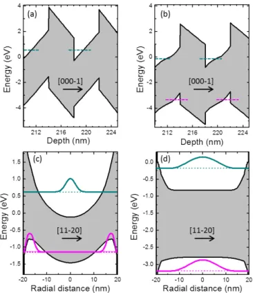
Le chapitre 5 porte principalement sur les propriétés optiques inter-bandes et intra-bandes des hétérostructures à base de nanodisques de GaN/AIN intégrés dans les NFs GaN avec différentes densités de dopage de germanium. Une partie importante de ce chapitre est l'étude des propriétés induites pa àl’ tatàdeà o t ai teàli eà àlaàp se eàd’u e o uilleàd’áIN.àDu point de vue optique, ces nanodisques présentent des temps de vie des porteurs d’environ 5 µs qui ne changent pas beaucoup avec la température. Ce phénomène a été attribué à l’a se e de défauts dans la région active de ces NFs et au confinement des porteurs en trois dimensions. Nous avons analysé les résultats des mesures de photoluminescence résolue en temps par comparaison avec des simulations tridimensionnelles de la structure électronique avec le logiciel Nextnano3. Nous avons ainsi démontré théoriquement une séparation des fonctions d'o deàdeàl’ le t o àetàdu trou le long l’a eà de croissance du NF et perpendiculairement à cet axe. L’aug e tatio àdeàlaàde sit àde dopage Ge dans ces structures conduit à une diminution des champs électriques radial et axial qui séparent l’ le t o àetàle trou. Cet alignement des fonctions d’ondes induit une diminution du temps de vie des porteurs de presque deux ordres de grandeur (publiés da sàl’a e eà ). En utilisant ces structures, nous avons également montré pour la première foisàl’absorption ISB dans les hétérostructures NFs, autou àdesàlo gueu sàd’o deàt l o .àL’ e gieàdesàt ansitions ISB peut être modifiée en changeant
la densité de dopage et l’ paisseu àdesà a odisques. Nos résultats montrent que les effets à N corps telsà ueàl’effetàd’échange ou l´écrantage par des plasmons sont des éléments essentiels à prendre en compte pou à e pli ue à ualitati e e tà lesà e giesà deà t a sitio à o se esà da sà l’i f a ouge (publiés dans l’annexe 7). La différence entre les dopants germanium et silicium est analysée par rapport à leurs effets sur l'absorption ISB dans ces NFs hétérostructurés.
Le chapitre 6 montre la possibilité de synthétiser les hétérostructures GaN/AIN sur les substrats non-polaires et semi-polaires. Nous avons analysé les transitions inter-bande et ISB dans les structures à PQs déposées sur les plans m-(1-100), a-(11-20) et (11-22) du GaN et nous avons comparé les résultats expérimentaux avec des calculs numériques. Par rapport aux plans non-polaires, nous avons observé une supériorité des PQs dits « plans m » par rapport aux structures « plans a » en termes de propriétés optiques et structurales. En nous focalisant sur les structures « plan-m », nous avons montré deà l’absorption ISB dans le domaine de 1,5-6,0 µm (publié dans l’annexe 8). De même, des mesures inter-bande et ISB dans les PQs GaN/AlN semi-polaires ont été publiées dans l’annexe 9.
Finalement, le chapitre 7 présente les conclusions de ce travail et apporte plusieurs perspectives en ce qui concerne la fabrication des lasers à cascade quantique et des détecteurs IR à base de NFs.
1
Table of Contents
Table of Contents ... 1
Glossary ... 3
. General Introduction ... 4
1.1. Motivation and targets ... 4
1.2. Organization of the manuscript ... 5
. Technical introduction ... 7
2.1. III-nitrides and their peculiarities ... 7
2.2. Quantum confined Stark effect ... 8
2.3. Intersubband transitions and the governing principles ... 9
2.4. Many body effects ... 12
2.5. State of the art for intersubband in nitrides ... 13
. Experimental methods ... 16
3.1. Material Growth and strain relaxation ... 16
3.2. Simulation parameters ... 18
3.3. Structural characterization ... 20
3.4. Optical characterization ... 20
. Results: c-plane THz intersubband devices ... 24
4.1. Introduction to THz intersubband ... 24
4.2. Intersubband absorption in GaN-based quantum wells (Annex 3, 4 and 5)... 24
4.2.1. The step-quantum-well design ... 24
4.2.2. The 4-layer quantum well design ... 26
4.2.3. The 4-layer pseudo-square quantum well design ... 27
4.3. Quantum cascade laser designs ... 28
4.4. Quantum cascade laser design constraints ... 29
4.5. Conclusions ... 32
. Results: Nanowires for intersubband devices ... 34
5.1. Introduction to nanowires ... 34
5.3. Understanding band-to-band dynamics (Annex 6) ... 35
5.4. Intraband absorption in nanowire heterostructures (Annex 7) ... 40
5.5. Note on silicon vs. germanium for n-type doping. ... 41
5.6. Conclusions ... 41
. Results: Alternate crystal orientations ... 44
6.1. Introduction to nonpolar and semipolar orientations ... 44
6.1. Optical: a- vs m- vs c-plane substrates ... 44
6.2. Structural: a- vs m- vs c-plane substrates ... 46
6.3. Longer wavelength intersubband transitions in the m plane (Annex 8) ... 47
6.4. Growth on semipolar substrates (Annex 9) ... 48
6.5. Conclusions ... 50
. Conclusions and prospects... 52
7.1. Conclusions ... 52
7.2. Prospects ... 53
7.2.1. THz quantum cascade laser fabrication ... 53
7.2.2. Nanowire intersubband technology ... 53
7.2.3. Nonpolar Intersubband devices ... 54
Bibliography ... 56
3
Glossary
Abbreviation Definition
2D two-dimensional
3D three-dimensional
ADF annular dark field
AFM atomic force microscopy
BEP beam equivalent pressure
FIR far-infrared
FTIR Fourier transform infrared spectroscopy FWHM full width at half of the maximum value HAADF High angle annular dark field spectroscopy HRTEM high resolution transmission electron microscopy HVPE hydride vapour phase epitaxy
IR infrared
ISB Intersubband
LED light emitting diode LO longitudinal optical
MBE molecular beam epitaxy
MIR mid-infrared
ML monolayers
MOCVD metalorganic chemical vapor deposition MOVPE metal-organic vapor phase epitaxy
MQW multi-quantum-well
n.i.d. non-intentionally doped
ND nanodisk - those inside nanowire heterostructures
NIR near-infrared
NW nanowire
PAMBE plasma-assisted Molecular beam epitaxy PL photoluminesence (spectroscopy)
QCD quantum cascade detector
QCL quantum cascade laser
QCSE quantum-confined Starck effect
QD quantum dot
QW quantum well
QWIP quantum well infrared photodetectors RHEED reflection high energy electron diffraction RMS root of the mean squared
SL superlattice
STEM scanning tunneling electron microscopy
TE transverse electric
TEM transmission electron microscopy
TM transverse magnetic
UV ultraviolet
.
General Introduction
1.1. Motivation and targets
Group III-nitride semiconductors have made the implementation of full-color optoelectronics possible due to their large direct band gap and doping capabilities; this has led to the development of blue and green light emitting diodes (LEDs). Heterostructures of these materials are found in the marketplace for a variety of applications, such as for blue laser diodes (blue ray players) or LEDs for household lighting. These materials are also currently used in high-power electronics because of their mechanical/thermal robustness [1], high electrical breakdown fields, and high electron motility. Furthermore, III-nitrides are currently the only solid-state alternative to mercury lamps as ultraviolet (UV) emitters [2]. By incorporating aluminum or indium into GaN, the bandgap of the material can be increased or decreased, respectively. The introduction of InGaN in solar cells has also attracted increasing interest because it can be optically active over a large spectral range – from the UV to the near-infrared (NIR) [3]–[7]. Finally, these materials are also becoming interesting due to their large conduction band offset [8], [9], large longitudinal optical (LO) phonon [10], [11] and their applicability to create devices in the IR by using intersubband (ISB) transitions [12].
In ISB devices, proper understanding of the electron and hole distribution and lifetime is crucial for the design of complex devices such as the quantum cascade laser (QCL) [13], [14]. The purpose of this work was to further the understanding of the manipulation of nanoscale systems with the intent of using these systems for ISB optoelectronic devices. An overarching goal for this thesis is to establish the knowledge base necessary and the basic units needed to manipulate III-nitride heterostructures towards the realization of a III-nitride-based QCL. This is done through conduction band engineering to accurately predict the ISB energy of these nanostructures from the NIR to the far-infrared (FIR).
This thesis aims to push the boundaries of GaN-based ISB technologies in a three-pronged approach focusing on c-plane GaN, in nanowires (NWs) and finally on nonpolar GaN:
Using polar c-plane technologies, we aim to define the building blocks that will lead to the creation of THz QCLs operating at room-temperature. By analyzing the inherent errors induced from the plasma-assisted molecular beam epitaxy (PAMBE) system, we created conduction band architectures eliciting ISB transitions in the THz spectral region which are insusceptible to these errors. These primary designs were improved upon, by taking into account both the tunability of the transition energy and tunneling transport requirements, in order to move forward towards complete devices. By analyzing the various GaN QCL designs based on GaAs materials, we have proposed a design specifically adapted to GaN.
Using NW structures, we aim to create ISB devices that can operate at high efficiencies for photodetection and eventually light emission/lasing. Towards this purpose, we have probed the effect of nanodisk (ND) size and doping on the interband and ISB characteristics of GaN/AlN NW heterostructures.
5 Finally, using alternative crystallographic orientations (nonpolar, semipolar), we aim to create heterostructure designs that can cover the full infrared (IR) spectral region with simplified band engineering through the reduction or cancelation of the polarization-induced electric fields. We have first analyzed various crystallographic orientations to decide which is better in terms of optical and structural performance. In view of the results, we have proceeded to explore the spectral capabilities of m-plane superlattices (SLs).
In this thesis, I engineered the conduction band profiles to target certain operating wavelengths from the NIR to FIR by simulating the structures using commercial nextnano3 software [15]. I was then in charge of the growth of these structures by PAMBE. Polar c-plane structures were grown by me, while off-plane structures were grown either by me or by PhD student Caroline Lim. In the case of NW heterostructures, growth was outsourced via collaboration with the group of Prof. Martin Eickhoff at the Justus Liebig University in Giessen (Germany). I optically characterized the c-plane samples and the NW heterostructures by photoluminescence (PL) and Fourier transform infrared spectroscopy (FTIR), and the off-plane samples were characterized in collaboration with Caroline Lim and Akhil Ajay. Time-resolved PL measurements were performed under the supervision of Dr. Joël Bleuse. Structural characterization was done in collaboration with Dr. Catherine Bougerol for transmission electron microscopy (TEM) of planar structures and the group of Prof. Jordi Arbiol in the Institut Català de Nanociència i Nanotecnologia, in Barcelona (Spain) for NW heterostructures. X-ray diffraction (XRD) spectroscopy was done with Dr. Edith Bellet-Amalric and Caroline Lim. Atomic force microscopy (AFM) images were procured in collaboration by Arántzazu Núñez Cascajero and Caroline Lim.
1.2. Organization of the manuscript
After this first chapter, which describes the motivation, targets and organization of the thesis, chapter 2 begins with a technical introduction of III-nitride semiconductors and their peculiarities, namely their crystal properties as well as the spontaneous and piezoelectric polarization fields arising from the strain relaxation mechanisms in GaN/Al(Ga)N heterostructures The physics behind ISB transitions are then presented, including the fundamental quantum mechanical equations involved. After this, the state of the art for ISB in III-nitrides is explored and the problems associated with its extension into the FIR are mentioned. Further information on the introduction of these technologies are also found in Annex 1 [16] and Annex 2 [17].
Chapter 3 outlines the experimental techniques used throughout the thesis. It first presents the PAMBE-growth of nanostructures including NWs, and the growth of planar heterostructures on nonpolar, polar and semipolar substrates.. It then outlines the parameters for the simulations performed on the thin film and three-dimensional (3D) heterostructures. Finally, it describes the structural and optical characterisation methods that were used throughout the thesis and how to properly treat the data to reach the conclusions obtained.
The results of the thesis are then introduced in three main chapters, associated with each of the three above-described targets. Chapter 4 covers THz structures grown on c-plane substrates. The existing architectures are theoretically analyzed regarding the errors induced within PAMBE growth.
A new design is then proposed and outlined in the two papers (Annex 3 and 4) [18], [19]. Annex 3 describes the inability to reproduce the previous designs, and the proposal for a new 4-layered multi-quantum-well (MQW) design is shown in Annex 4. Because this system was so robust, it was hard to vary the ISB wavelength. By keeping in mind the robustness and the tunneling transport requirements for incorporating these designs into QCL architectures, a pseudo-square design is introduced in Annex 5 [20]. The chapter finishes with a review of existing QCL designs and demonstrates that this pseudo-square design can be used as the building block in LO-phonon-based QCLs.
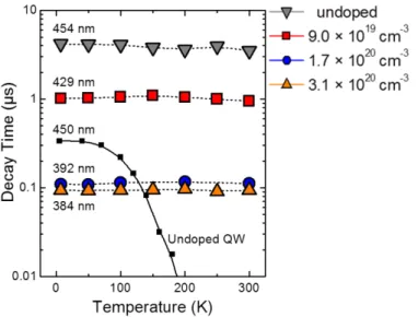
In chapter 5, NW heterostructures are first explored from an interband approach by using temperature-dependent and time-resolved PL, interpreted by comparison to calculations of the quantum mechanical structure. The main results are presented in Annex 6 [21] and show that the carrier lifetime can be varied over two orders of magnitude by changing the doping level. The ISB properties of these structures are also probed as a function of ND thickness and dopant level. The strain state, eigenfunctions, and ISB properties were simulated, and the results are shown in paper Annex 7 [22].
Chapter 6 starts by comparing the growth of a-, m-, and c-plane GaN/AlN SLs by analyzing their structural and optical properties. In terms of mosaicity, surface roughness, PL linewidth and intensity, and ISB absorption, the m-plane SLs were deemed to be the best nonpolar choice. This then led to the design of heterostructures with ISB transitions in the mid infrared (MIR) described in Annex 8. Semipolar planes were also explored for ISB applications, and showed that GaN/AlN MQWs could be fabricated with ISB transitions spanning the NIR as explained in Annex 9 [23].
Finally, chapter 7 contains the conclusions of the thesis and comments on the next steps to be taken for each of the three targets, including the processing of QCLs, NW photodetectors, and nonpolar architectures for quantum well infrared photodetectors (QWIPs), and how to integrate them into existing GaAs device architectures moving towards the FIR.
7
.
Technical introduction
2.1. III-nitrides and their peculiarities
AlN and GaN were first synthesized in 1907 by crystalline sublimation [24], and in 1931 by reacting ammonia gas with metallic gallium [25], respectively, and were first made by molecular beam epitaxy (MBE) in 1975 for AlN [26] and 1969 for GaN [27]. N-type doping is accomplished primarily through the use of Si [28], and p-type doping, albeit less effectively, is accomplished by using Mg [29].
GaN has been grown heteroepitaxially on a variety of substrates including SiC, Si, and Al2O3. Various companies are supplying bulk GaN grown by HVPE [30, p. 196], ammonothermal [31], or other methods, for optical devices such as laser diodes or to sell as substrates (see Table 1).
Company Product Growth method
Soraa GaN Ammonothermal [32]
Hamamatsu GaN HVPE on patterned substrates [33]
Hexatech AlN Physical vapor growth [34]
Lumilog GaN HVPE [35]
Ammono GaN Ammonothermal [36]
Seren Photonics semi- or nonpolar GaN (templates) MOCVD [37]
Sumitomo/Soitec GaN HVPE [38], [39]
Nanowin Polar/nonpolar/semipolar GaN HVPE [40] Table 1 Various companies producing GaN substrates
In this work we will focus strictly on GaN, AlN and the ternary alloy of AlGaN. (Al,Ga)N can be grown in cubic (β àzincblende phase as well as the hexagonal (α wurtzite phase. This work deals entirely with the αàphase,à hi hàisàtheà ostàthe od a i all àsta le.àThe wurtzite crystal structure is described through the use of four miller-Bravais indices (hkil). Where h,k, and i are separated by 120° and sit perpendicular to the c axis. The c plane (0001), the m plane (10-10), and the a plane (1120) are indicated in Figure 1.
The [0001] axis is considered positive when the <0001> vector along the bond between the Ga and N points from the metal atom to the nitrogen atom. Conventionally, (0001) crystals are called Ga-polar and are typically preferred over (0001) N-polar as they are more chemically stable and their surface morphology can be more easily controlled during the growth.
Because of the low symmetry of the crystal, the gravity centres of the positive and negative dipoles do not coincide and there is therefore a spontaneous polarization field along the <0001> axis. Because this has a dependency on the ideality of the crystal, the cation-nitrogen bond length, and the chemical properties of the cation [41], there is a difference in the magnitude of polarization for GaN and AlN. GaN has a spontaneous polarization value (-0.029 C/m2 [41] or -0.034 C/m2 [42]) smaller than AlN (-0.081 C/m2 [41] or -0.090 C/m2 [42])as a result of the larger crystal non-ideality
i.e. the larger on-axis bond length, and lower aspect ratio unit cell, as well as the larger effective charge and chemical nature of the cation. This spontaneous polarization is a determining factor for the creation of devices and is also the reason that interband devices can function at energies below the bandgap of GaN.
A piezoelectric polarization is also present in a GaN/AlN heterostructures that is linearly dependent on the strain field present within the material. Stress leads to deformations in the lattice a o di gàtoàHooke’sàla :
� = ∑ �
where is the elastic tensor, and σàa dàε represent the stress and strain respectively. is transformed to by replacing m,n = {xx, yy, zz, yz, zx, xy} with m,n = {1, 2, 3, 4, 5, 6}. Due to crystallographic symmetry, many of the tensors within are 0, and the matrix can be represented by 5 independent tensors such that C11=C22, C12=C21, C13=C31=C23=C32, C33, C44=C55,
C66=0.5(C11C21) [43], [44], [45, p. 199], [46]–[50] and the values can be seen in Table 3.
In the case of biaxial stress of a material grown along the [0001] direction (� = and � = � , the strain-induced piezoelectric polarization (Ppz) can be expressed as:
�� = � ( − ) = � − �� ( − )
where a and a0 represents the out-of-plane lattice parameters of the strained and bulk materials,
and e31 and e33 represent the piezoelectric constants from the piezoelectric tensor. The values for these can be seen in Table 3.
Calculations for strain distribution in 3D structures are more complex in contrast to planar structures. For instance, in the case of NW heterostructures, the strain distribution is numerically calculated by assuming relaxation to the minimum total elastic energy and zero-stress boundary conditions at the surface.
2.2. Quantum confined Stark effect
The most common orientation for growing GaN is along the [0001] direction. This is because it has uniform atomic composition in that layer; the top is either Ga or N. This growth direction is aligned with the spontaneous polarization in the material, which, in heterostructures generates internal electric fields and phenomena such as the quantum confined Stark effect (QCSE). When electrons and holes are confined in a QW, the internal electric field shifts the electron states to lower energies, while the hole states are shifted to higher energies, reducing the permitted light absorption and emission frequencies. Additionally, the external electric field within the quantum well (QW) shifts electrons and holes to opposite sides of the well, decreasing the overlap integral, which in turn reduces the recombination efficiency of the system.
Growth of GaN in nonpolar (perpendicular to the spontaneous polarization vector) and semipolar (inclined with respect to the spontaneous polarization vector) orientations has been mainly motivated by the reduction of the QCSE, and started in 1987 [51]. By growing on nonpolar planes,
9 the internal electric field is null along the growth axis, while for semipolar planes, it is greatly decreased.
Figure 1 (a) shows a schematic of the growth planes of the wurtzite crystal and the associated band structure and wavefunctions for heterostructures of GaN/AlN grown along the (b) c and (c) nonpolar crystal orientations.
Figure 1 (a) Schematic diagram of various planes within a hexagonal unit cell: m plane (1-100) , a plane (11-20) and c plane (0001). (b) Band diagram schematics for c-plane AlN/GaN/AlN QWs. The internal electric field within c-plane GaN causes asymmetry in the wavefunctions. (c) Band diagram for a/m-plane AlN/GaN/AlN QWs. This asymmetry is not present in the a/m-plane QW due to the absence of the internal electric field.
Nonpolar GaN has been used in devices since 2000, with the first demonstration of a laser diode using nonpolar m-plane [52] and a-plane GaN [53] in 2003. Research has since expanded to a number of avenues including quantum dots (QDs) [54], [55], AlGaN/GaN MQWs [56], InGaN/GaN [57], [58], thicker films of GaN [59]–[61] or AlN [62], as well as to devices such as LEDs [63], lasers [64] and transistors [65]. However, for nonpolar growth, there is strong anisotropy of the surface properties resulting in layers with high defect densities. A compromise to this is seen with semipolar planes [66].
Initial research on the growth of semipolar GaN was driven by the need for longer wavelength laser diodes in the green [67], [68] and violet, as well as longer wavelength LEDs reaching the red and amber [69]–[71]. It has since shown promise in its ability to more easily incorporate indium [72]–[75], and has led to the creation of various start-ups like Soraa and Kaai [76], [77].
Substrates for epitaxial growth have been the main challenge for these systems and the best performing devices have been obtained using substrates acquired by slicing HVPE GaN boules along the nonpolar and semipolar planes. Research has also been done to create semipolar GaN using preconditioned templates [78]–[84].
2.3. Intersubband transitions and the governing principles
Semiconductors can be made optically active at IR wavelengths by engineering the quantized confinement of the electronic levels in QWs, NWs or QDs. QCLs or QWIPs are well-known illustrations of quantum-engineered devices. These controlled-by-design devices rely on optical ISB transitions between quantum-confined states, either within the conduction band or within the
valence band. The desired wavelength of operation can be obtained by a proper choice of the layer thicknesses and compositions.
The first ISB transitions were seen in an n-doped Si system in 1974[85]. Since then, ISB absorption has moved to other materials, including GaAs [86], [87], and the III-nitrides[88].
ISB transitions are governed by selection rules: to interact, incoming light needs to have an electric field in parallel to that of the heterostructure (perpendicular to the semiconductor layers). This imposes the use of TM polarized light, and necessitates the use of waveguides or surface gratings to couple light into the active region. Furthermore, due to the inversion symmetry, only transitions between wavefunctions of opposite parity are allowed.
A comprehensive introduction to ISB physics in QWs can be found in the works of Bastard [89] or Liu and Capasso [14]. In this section, we briefly introduce the polarization selection rule characteristic of ISB transitions. For this purpose, we consider a QW with two confined states in a single-particle approach. Transition rates W from states i to f a eàdes i edà àFe i’sàgolde à uleàasà follows:
= ћ |⟨� |�′|� ⟩| ( − − ћ )� (1)
whe eàH’àisàtheài te a tio àHa ilto ia ,àEi and Ef and Ψi and Ψf are the energies of confinement levels and wavefunctions of the initial and final states respectively, and ћω is the influencing radiation energy. As the radiation wavelength is much larger than the QW width in the case of IR radiation, a dipole approximation can be applied to the Hamiltonian.
�′=
∗ � ∙ � (2)
where q the elementary charge; Fo is the amplitude of the electric field; m* the effective mass; ω the wavelength of light, and �, and � the polarization and momentum operators respectively.
=�ћ ∗ |⟨� |� ∙ �|� ⟩| ( − − ћ ) (3)
By expressing the wavefunctions as products of periodic Bloch functions, u, and a slowly-varying envelope functions, f, the transition rate can be shown:
=�ћ ∗ | � |� ∙ �|� ′ ′ | ( − − ћ ) (4)
where b and b’,à a dà s and s’à a eà theà a dà a dà su a dà i di esà ofà theà i itialà a dà fi alà states,à respectively. This can be expanded to give:
11 The first term describes interband transitions (if b≠b’ then � |� ′ ≈0). The second term describes the ISB transitions (if b=b’ then the first term vanishes and � |� ′ =1). This leaves ISB transitions to be governed by |�| ′ .
The motion of electrons in x and y inside thin film structures grown along the z axis by assuming a Bloch wavefunction for both the well and barrier and assuming �′= :
⃗ = √
⃗⃗ ��⃗� � (6)
where �⃗⃗ � and ⃗ are the two-dimensional (2D) wave vector and the position vector respectively; A is the sample area and � is the envelope function component along z. This follows to a substitution to obtain the ISB dipole matrix element:
⟨ ⃗⃗ �|� ∙ �| ′ ′⃗⃗⃗⃗⃗�⟩ = ∫ − ⃗⃗ ��⃗�∗ � [� � + � � + � � ] ⃗⃗⃗⃗⃗′ ��⃗�′ � (7) upon substitution into Equation 3, taking into account that �⃗ ′= � × ⃗ ′ we can rewrite the transition rate as follows:
= �⃗⃗ �− �′⃗⃗⃗⃗ � � ћ | | | �∗ � |�| � ′ � | ( − − ћ ) (8) From equation 7; terms containing � or � vanish unless s=s’ and �⃗⃗ �= �′⃗⃗⃗⃗ � (identical states). Equation 8 contains the first delta function to conserve these momentum requirements. Also, because of the presence of , only electric fields in the z direction couple to discrete energy levels of the QW. This is the basis for the polarization selection rule which leads to the use of waveguides and surface gratings, and why only transverse magnetic (TM) polarized light interacts with the energy levels. Furthermore, transitions between states with the same wavefunction parity are not allowed – this is only the case for symmetric QWs.
Under the assumption that the lattice periodic function is the same in all constituent materials, a Schrödinger equation only for the envelope function can be derived with the goal to isolate the eigenenergies.
−ћ
∗∇ ∙ ⃗ + ⃗ ⃗ = ⃗ (9)
Substituting the values for ⃗ from Equation 6, and solving the differential equation leads to the energy eigenvalues of the form
where depends on the potential profile � . For symmetric QWs with infinite barriers, the following eigenvalues are obtained:
� � = √�sin ��� � (�⃗⃗ �) = ћ �
∗� + ћ �⃗⃗ �
∗ (11)
where L is the QW thickness. Due to the large effective mass of GaN (m*/m0 ≈ 0.2) [90], versus GaAs(m*/m0 ≈ 0.067) [91], or InAs (m*/m0 ≈ 0.023) [92], very thin QWs are required in the for large ISB energies
2.4. Many body effects
The transition between quantum-confined states relies on the fact that one of the states must be populated. In the case of absorption this requires the use of doping to occupy the ground state of the QWs [93] and this elicits many-body effects such as the depolarization shift, the exchange interaction, or the screening of the internal electric field.
The depolarization shift (also known as plasmon screening) and the exciton shift introduce a correction to the ISB energy that can be expressed by:
̌ ′ = ′ √ + − (12)
where α and β correspond to the depolarization and exciton shifts, respectively, and Es’s to the ISB energy between states s’ and s.
The depolarization shift is due to the external radiation interacting with the electron plasma, which leads to a modulation of the carrier density and an increase of the transition energy, which can be estimated as [13] = � ′ − � ∫ � [ ∫ �′�′ �′ � �′ −∞ ] (13)
where � is the sheet carrier density, the dielectric constant, 0 the permitivity of vacuum. The second half of the expression represents the ISB coulomb integral for laterally homogeneous systems.
Additionally, the exciton shift arises from the interaction between the excited electron and the ground-state hole [94].
β =− �
′ ∫ � � ′ � � � � � (
�
13 where A=21, B=0.7734 [13], [94], m* is the effective mass, = [ � � � � ]
−
, � � is the 3D electron density such that ∫ � � = � and aB is the Bohr radius.
The exchange interaction accounts for the electron repulsion between electrons with parallel spin as a result of the Pauli principle. This acts to lower the energy of the highly-populated ground state and red shifts the interband, but blue-shifts the ISB. This effect is directly proportional to the dopant concentration in the level, and via a Taylor series expansion can be represented as [95], [96]:
ℎ � = − �� [�� � − .� ��
� ] (15)
where kL is equivalent to �
�, LàisàtheàQW’sàthi k ess,àE is the elliptic integral, and � = √ �� . The direct Coulomb interaction is as a direct result of Coulomb-Coulomb interactions and tends to screen the internal electric field. It is given as follows [95], [97]:
� = � � �
(16)
Taking into account the summation of the above-described many-body effects, the ISB transition energy can be estimated as:
′ = ′ (√ + − ) − ℎ− � (17)
2.5. State of the art for intersubband in nitrides
III-nitride semiconductors (GaN, AlN, InN and their alloys), with their wide band gap and a large conduction band offset (~ 1.8 eV for GaN/AlN [98]–[100]), have been attracting much interest for ISB devices operating from the NIR to FIR spectral range. GaN is transparent in a large spectral region, notably for wavelengths longer than 360 nm (band gap), except for the Reststrahlen band (from 9.6 à toà µm). Absorption in the range of 7.3 µm to 9 µm has been observed in bulk GaN substrates with carrier concentrations <1016 cm-3 [101]–[103], and was attributed to the second harmonic of the Reststrahlen band. Although this absorption might hinder the fabrication of waveguided devices in this spectral region, its effect in planar devices with µm-sized active regions is negligible, since the absorption coefficient related to two-phonon processes is much smaller than the one associated with ISB transitions [104], [105]. Conversely, III-nitrides do not present problems of inter-valley scattering, since the L and points are much higher in energy (>2 eV) than the point.
Various review articles have been written following the evolution of the GaN-based ISB technology [16], [17], [106], [107, p. -], [108]–[110]. The first observation of ISB absorption in GaN/AlGaN QWs was published at wavelengths above 2.8 µm [88] in 1999. The wavelength was then
tuned down to 1.75 µm [111] and finally ISB was seen around the telecommunication wavelength of 1.55 µm [112] in 2000. Since them, ISB transitions have been observed at room temperature in nitride-based QWs and QDs by a number of groups (University of Paris-Sud, Bell Labs, Nothwestern Univ., Univ. of Boston, Cornell Univ., Univ. of Tokyo, Sophia Univ., Toshiba Corp., CHREA-CNRS, EPFL, Chalmers Univ. of Technology, Univ. of Magdeburg, and CEA-INAC).
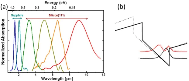
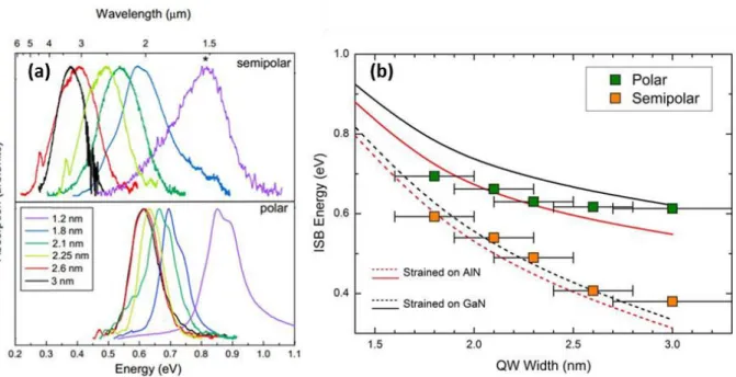
Figure 2 (a) Normalized absorption spectra for various samples showing that ISB transitions can span from the NIR to the MIR. The substrates used for these samples are also noted above the respective wavelength ranges.
(b) An illustration of the QCSE where the well width of a GaN well is changed by 30%. With an increase in the
well width by 30%, a decrease in the ISB energy of less than 3% is seen.
Besides the telecommunications range, there has also been interest to create devices towards longer wavelengths. Using GaN/AlN QWs, the e2-e1 ISB transition can be tuned in the 1.0 to 3.5 µm wavelength range by changing the QW thickness from 1 nm to 7 nm [100], [113]–[120]. By using AlGaN instead of AlN in the barriers, the wavelength range can be extended further into the MIR up to 10 µm [93], [121]–[126] as seen in Figure 2 (a). However, for larger QWs (>5 nm), the first two confined electron levels get trapped in the triangular section of the QW, which results in a saturation of the e2-e1 value by the QCSE, as seen in Figure 2 (b).
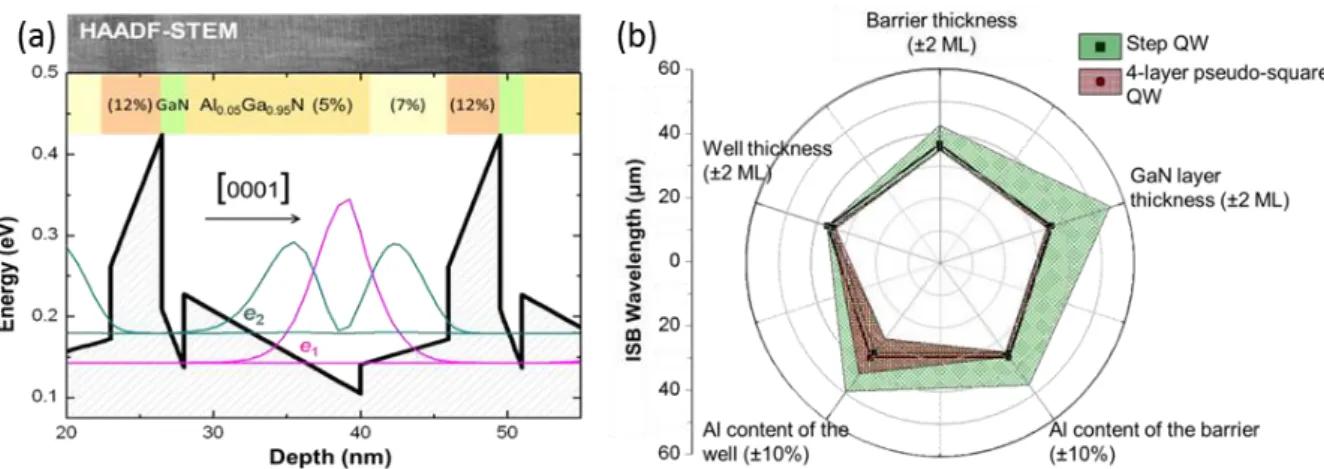
To further reduce the ISB transition energy, Machhadani et al. [127] proposed an alternative strategy to approach a flat potential in the QW layers by engineering the internal electric field. The investigated structures contain a stack of step-QWs, each period consisting of a GaN well, an Al0.05Ga0.95N step barrier and an Al0.1Ga0.9N barrier. Transmission measurements performed at 4 K reveal TM-polarized ISB absorption at 70 and 150 µm.
The first prototypes of nitride-based ISB devices were room-temperature multi-Tbit/s all-optical switches operating at 1.5 µm [128]. Meanwhile, the first demonstrations of III-nitride photovoltaic and photoconductive QWIPs and QD IR photodetectors were demonstrated in 2003 [129], [130] and 2006
[131]
–[133]
respectively for NIR frequencies, and in 2010 in the FIR [134]. Ultrafast all-optical switches have also been demonstrated [128], [135]–[138]. The first evidence of strong electron coupling in GaN/AlN double QWs [139] led to the demonstration of the first charge-transfer GaN-based ISB electro-optical modulators [140]. Finally, NIR ISB luminescence from GaN/AlN QWs [141]– [143] and QDs [144] was detected. The concept of quantum cascading in III-nitrides has also been15 demonstrated through the development of QD-based quantum cascade photodetectors (QCD)s operating in the 1.5-2.0 µm spectral range [145], [146], which opens prospects for QCLs.
.
Experimental methods
3.1. Material Growth and strain relaxation
The growth of III-nitrides has occurred in a variety of instruments, each with their own particular benefits and drawbacks. Table 2 lists the typical machines used to grow GaN and AlN, including metalorganic vapor phase epitaxy (MOVPE) / chemical vapor deposition (MOCVD), hydride vapor phase epitaxy (HVPE)[30], MBE and reactive sputtering.
MOVPE/ MOCVD
Precursors: Mixtures of trimethylindium, -gallium, or –aluminium ((CH3)3M), and NH3 [147]
Growth temperature: 1000-1100°C [148]–[150]
Results: High growth rate (1-3 µm/h) and excellent material quality and control over layer thickness and doping.
HVPE Precursors: GaCl, NH3 [151]
Growth temperature: 1000-1050°C [148], [152]–[154]
Results: Very high growth rate (up to 100 µm/h). Possibility to synthesize mm-thick GaN crystal boules to slice free-standing wafers [155].
MBE Precursors: High purity metals and N2 or NH3 Growth temperature: 700-800 [156]
Results: very low growth rate, excellent control over layer composition. Can start and stop the growth of layers with atomic precision as well as the flux of a specific atom giving layer-by –layer control over the alloy concentration and thickness. Furthermore, in-situ reflection high-energy electron diffraction (RHEED) characterization greatly helps to characterize the growth. Gas-MBE also exists, which uses ammonia or hydrazine for the N-precursor.
Sputtering Precursors: High purity metals or III-nitride blanks and N2 Growth temperature: 300-750°C
Results: lower crystal quality but deposition is possible in any substrate and in large surfaces. [157]
Table 2 List of methodologies used to grow GaN and AlN.
The samples studied in this thesis are grown strictly using PAMBE. Substrates for m-plane and a-plane exploration consisted of free-standing GaN sliced along nonpolar surfaces from (0001)-oriented GaN boules synthesized by HVPE by Nanowin (Suzhou Nanowin Science and Technology Co., Ltd). The semipolar substrates consisted of 2-µm-thick (11-22)-oriented GaN layers deposited on m-sapphire by MOVPE by Dr. Ph. de Mierry and Dr. G. Nataf at CRHEA-CNRS [75]. In the case of c-plane GaN/Al(Ga)N heterostructures, growth was performed on 1-µm-think AlN-on-sapphire templates (for NIR structures) or on 4-µm-thick GaN-on-Si(111) templates (for MIR structures), both deposited by MOVPE by Dowa Electronics Materials Co., Ltd. For the fabrication of devices operating in the NIR (1.3-3 µm), the use of AlN-on-sapphire templates is preferred to maintain the structure under compressive strain and thus prevent crack propagation. For devices operating beyond 3 µm, GaN-on-Si(111) substrates are preferred to guarantee IR transparency of the substrate [125].
17 The RHEED was the main in-situ measurement tool used to calibrate and ensure epitaxial quality of all the samples grown in this thesis. By analyzing the diffraction pattern, the surface roughness, in-plane lattice constants, and the surface morphology could be established. Measuring RHEED intensity oscillations, the growth rate can be deciphered. Furthermore, by timing the desorption time of the Ga excess on the GaN(0001) surface, the substrate temperature could be estimated.
This thesis focuses on GaN, AlN and the ternary alloy AlGaN. It is also possible to grow InGaN and InN heterostructures, which would be theoretically preferred to develop an ISB technology due to the much lower electron effective mass of InN. However, In-containing technologies are penalized by the large lattice mismatch between GaN and InN, severe alloy inhomogeneities and interdiffusion/segregation at the InGaN/GaN interfaces [158], [159]. Therefore, the GaN/Al(Ga)N system is a more feasible solution for ISB devices.
The growth of (0001)-oriented GaN, AlN and AlGaN by PAMBE is extensively discussed in the literature [160]–[166]. For the growth of GaN using PAMBE, the Ga/N ratio is a critical parameter that directly influences the surface morphology. Too low of ratio result in a rough, facetted surface morphology [162], too high and Ga accumulates on the surface. Thin films of GaN in this thesis are always grown under slightly Ga-rich conditions, where the Ga flux was set to a value slightly below the limit of accumulation. In this mode two monolayers (ML) of Ga form on the surface of the sample in a dynamic equilibrium [160], [161], [168]–[170], and is stable for growth temperatures above 700°C [167]. These growth conditions have been theoretically explained through the creation of an efficient diffusion channel underneath a thin metal layer on top of the growing surface [161], [168], and have been proven to improve the surface morphology and decrease the defect density [167], [171]. The substrate temperature was around 720°C as deduced from the Ga desorption time[160], and the growth rate was determined by the flux of nitrogen and was in the range of 0.3 to 0.5 ML/s.
In the case of AlN, the deposition of layers with atomically flat surface morphology also requires metal-rich conditions [165]. However, Al does not desorb from the surface at the standard growth temperature for GaN. Therefore, to eliminate the Al excess at the surface, it is necessary to perform periodic growth interruptions under nitrogen. Due to the preferential incorporation of Al into the crystal over Ga [125], [163], [172], alloys of AlGaN can be created without having to remove the Ga-bilayer. By opening the Al shutter, a flux of Al is incorporated into the GaN growth that displaces the Ga atoms. For example, when growing Al0.05Ga0.95N, a flux of Al at 5% of the flux of N is used.
The PAMBE growth of NWs was initially demonstrated on sapphire [173], [174], then on Si[175].The NWs from this thesis were grown by PAMBE on Si(111) substrates at a temperature around 790°C [176]–[180] using a Ga/N ratio of 0.25 [181]. They are grown catalyst-free in the <000-1> direction (N-polar) [182]. These NWs are hexagonal prims with m-plane facets [183], [184]. NW growth proceeds from two angles, either by direct material deposition, or through the diffusion of atoms along the wire sidewalls to the apex [180], [185]–[187]. The marker technique showed that growth occurs under different circumstances than with 2D layers due to the negligible diffusion of N atoms [171], the Ga diffusion from the sidewalls and 3D nature of the growth [188], [189] which
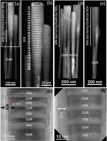
contribute to the faster axial growth rate over 2D layers. For growing heterostructures using AlN, the diffusion of Al was found to be insignificant [186], [188], and this contributed to the natural formation of an AlN shell. GaN/AlN heterostructures have been demonstrated axially [174], [190]– [193], and radially [186], [188], but growing radial heterostructures has the drawback of a shadowing effect [194], [195] that is difficult to overcome [196].
Nonpolar Growth began in 2000, with the growth of m-plane (10-10) GaN on γ-LiAlO2 [52]. Since then, the growth of nonpolar GaN has been well studied. a-plane GaN has been grown on r-plane sapphire [53], [197]–[201], and a-plane SiC [202], whereas m-plane GaN has been grown on m-plane SiC [203]. However, in 2006 efforts to grow these materials refocused towards substrates cut from HVPE-grown boules [204], [205]. This thesis focuses on these free-standing m- and a-plane GaN substrates. For on-axis m-plane substrates, the problem of hillocks plagued the growth [206], and was drastically reduced by incorporating a miscut in the c direction above 0.45° [207], above 0.7°[208], or 1°[209]. Due to the anisotropy in nonpolar crystal orientations, there is a higher risk of generating basal plane stacking faults [59], [198], [210].
Semipolar GaN can be grown in numerous crystal orientations, such as (10-11), (10-1-3) (11-22) on substrates such as (100) and (110) spinel [211] or on m-plane sapphire [66], [211]. In the case of (11-22)-oriented GaN grown by PAMBE, a Ga coverage independent of exposure time is only observed for a Ga coverage below 1 ML [212]–[214], and smooth GaN is theoretically predicted to grow in N-rich conditions [214]. However, optimized surface morphology is seen when there is a Ga-excess of 1 ML [215]. By growing directly on m-plane sapphire, the structures should be grown under Ga-rich conditions for streaky RHEED patterns, as III/V ratios smaller than unity lead to 3D growth [215]. This direct growth also results in metal-polar [210] samples containing two crystalline orientations [215]–[217]. However, by growing on an AlN buffer, a reduction in the secondary crystalline orientation is seen [215]. The growth of AlN on m-sapphire is either (11-22) or (10-10) depending on the III/V ratio [66] where, higher III/V ratios lead to larger inclusion of (10-10) crystals [66]. Rougher surfaces are seen when the III/V ratio strays from unity, and (10-12) AlN is optimally grown at a III/V ratio of about 0.85 [66]. In this thesis, the GaN was grown in the (11-22) direction on top of 2-µm-thick (11-22)-oriented GaN layers deposited on m-sapphire by MOVPE [75]. The growth rate of the PAMBE setup was set to 0.3 ML/s at a growth temperature of 715°C [215].
3.2. Simulation parameters
The simulations of the strain state, band diagram and electronic levels were performed using nextnano3 [15], taking the spontaneous and piezoelectric polarization into account. For thin films, the 8x8kp Schrödinger-Poisson solver was used self-consistently. The k·p theory model overcomes the assumption of parabolic band structures that are usually considered for convenience at the bottom of the conduction band and the top of the valence band. By incorporating this non-parabolicity, differences in ISB energy of up to 25% can be seen [218].
As GaN/AlN is a lattice mismatched system with an in-plane lattice mismatch of 2.5%, the effect of strain and lattice relaxation plays a defining role in both the device functionality as well as the band structure. Additionally, GaN/AlGaN heterostructures are very sensitive to the piezoelectric
19 fields, which make the calculation of the strain state of GaN/Al(Ga)N heterostructures crucial for understanding the electric fields and therefore the band profiles. The effect of the strain state has two main effects on the band diagram: Firstly it changes the band gaps of the materials, and secondly it changes the piezoelectric polarization within the materials. This induces changes in both the interband and ISB energies.
Parameters GaN AlN
Lattice constants, nm [109, p. 200] a c 0.31892 0.51850 0.3112 0.4982 Spontaneous polarization, Cm-2 [41] -0.029 -0.081 Piezoelectric constants, Cm-2 [41] e13 e33 -0.49 0.73 -0.60 1.46
Elastic constants, GPa [45], [47]
C11 C12 C13 C33 390 145 106 398 396 140 108 373 Dielectric constant[219] 10 8.5 Luttinger parameters[220] A1 A2 A3 A4 A5 A6 A7 // P E [eV] P E [eV] -5.947 -0.528 5.414 -2.512 -2.510 -3.202 0 14 14 -3.991 -0.311 3.671 -1.147 -1.329 -1.952 0 17.3 16.3 Deformation potentials, eV [219] ac1 ac2 D1 D2 -4.6 -4.6 -1.70 6.30 -4.5 -4.5 -2.89 4.89 D3 D4 D5 D6 8.00 -4.00 -4.00 -5.66 7.78 -3.89 -3.34 -3.94 Band offset, eV [218] 1.8
Table 3 The material parameters used in the theoretical calculations in nextnano3. The sources for each parameter are shown beside the parameter name.
In the case of 3D calculations, the effective mass approximation was used so that the simulations would converge at useful spatial resolutions. Simulations were done step-wise: The 3D strain distribution was first calculated by minimizing the elastic energy and applying zero-stress boundary
conditions at the surface. With this input, the nonlinear Poisson equation was classically solved to obtain the 3D band structure of the complete wire. After the Poisson equation was solved in equilibrium, the eigenfunctions were calculated by solving the Schrödinger equation in a quantum region that covered one ND in the center of the NW, including the AlN barriers on the top and bottom. nextnano3 does not completely incorporate many-body effects, and for calculations at high dopant levels, only the screening of the internal electric field is taken into account.
3.3. Structural characterization
The structural characterisation of the samples was done employing various methods to show the macro- and microscopic properties of the materials:
The periodicity of the samples was analyzed by XRD under the supervision of Dr. Edith Bellet-Amalric, using a Seifert XRD 3003 PTS-HR system. Typical samples had θ- θ scans of the (0002) reflections done to determine the SL periods. The experimental measurements were then ju taposedàtoàsi ulatedà u esào tai edàf o àX’Pe tàEpita àsoft a eàf o àPa al ti alàa dàaàSL misfit strain relaxation could be calculated. Additional information of the strain state was extracted via reciprocal space maps.
The surface roughness of the layers was measured by AFM in the tapping mode with a Veeco Dimension 3100 microscope. Data visualization and processing were carried out using the WSxM software [221].
For planar structures, TEM studies were realized by Dr. Catherine Bougerol using the microscopy facilities of CEA/INAC. For NW heterostructures, TEM images were provided by the group of Prof. Jordi Arbiol in the Institut Català de Nanociència i Nanotecnologia, in Barcelona (Spain).
3.4. Optical characterization
Optical characterization of the samples was mostly used to identify ISB transitions via FTIR spectroscopy, and band-to-band transitions via PL techniques.
FTIR was used to probe the ISB absorption using a variety of lamps and photodetectors incorporated into a Bruker V70v spectrometer. The source, beam-splitter and detector for each spectral range (NIR, MIR and FIR) are summarized in Table 4.
NIR MIR FIR
Source Tungsten Globar Hg-Arc
Beam-splitter CaF2 KBr Si
Detector MCT MCT Bolometer
Temperature of sample Room (300 K) Room (300 K) Liquid He (5 K) Temperature of detector Liquid Nitrogen (77 K) Liquid Nitrogen (77 K) Liquid He (5 K)
Table 4 Source, beam-splitter and detector used to measure ISB absorption in the NIR, MIR and FIR. The temperatures of the samples and detectors are also noted.
21 For their characterization, all samples grown on silicon-based templates were polished into multi-pass waveguides with 30° facets. The angle was chosen so that the light impinging the waveguide perpendicular to the facet had numerous interactions with the GaN, even in the case of a small deviation of the incidence angle. Figure 3 (a) shows the schematic of the waveguide where and the light is incident on the GaN from the Si. Focusing at the Si/GaN interface, light incidence angles below 49° (red) result in total reflection at this interface, i.e., the light does not transmit into the GaN layer. Incidence angles between 49° and 73° (green) lead to transmission into the GaN and total reflection at the GaN/air interface. Finally, incidence angles larger than 73° (orange) lead to transmission through the GaN into the air. Therefore, nominal incidence at 60° is chosen (i.e. normal incidence to a 30° facet). If we consider now the deflection of the light at the Si/air interface, the analysis is depicted in Figure 3 (b). For incidence angles below 18°, there is total reflection at the GaN/Si interface, whereas for incidence angles larger than 18°, light transmits into GaN and there is total reflection at the GaN/air interface. Transmission to air does not happen at any angle. Therefore, our choice of 30° facet allows light incidence in a large range of angles (18° to 180° as described in Figure 3 (b)). These al ulatio sà e eà adeà a o di gà toà “ ell’sà la à assu i gà theà refractive index of air to be 1, Si to be 3.48, and GaN to be 2.316 (1.55 µm). Following a similar reasoning, samples grown on sapphire-based templates or bulk GaN were polished at 45°.
Figure 3 Schematic of the interaction of light with the multi-pass waveguide where the Si is depicted in yellow and the GaN-based active layer is depicted in white. (a) Reflection/transmission behavior at the silicon/GaN interface as a function of the angle of incidence. The orange region (90°>θ>73°) depicts the angles where light enters the GaN is transmitted to the air. The green region (73°>θ>49°) depicts the angles where there is total internal reflection at the GaN/air interface. The red region (49°>θ>0°) depicts angles where there is total reflection at the Si/GaN interface (no interaction with the active layer). (b) Schematic of the light transmission at the air/Si interface (30° facet). Angles <18° lead to total reflection at the GaN/Si interface.
The samples were tested in transmission mode using a polarizer to discern between the transverse-electric (TE) and TM polarized light. By taking the selection rules into account, the ISB absorption should appear as a dip in the TM transmission spectrum. In the case of FIR characterization, two sample pieces were placed back-to-back to double the amount of surface perpendicular to the incoming beam, and to increase the detected signal.
For samples exhibiting ISB activity in the FIR, a trade-off between the absorption intensity and the FTIR signal i te sit àisào se ed.àátàlo àa glesàofài ide eà °<θ< ° àthe eàa eàfe e ài te a tio sà
between the light and the active layers which leads to larger amounts of light reaching the bolometer. A larger absorption is seen at high angles of incidence, but it is associated with a poor signal-to-noise ratio. An easy approach to identify the ISB absorption was to monitor the TE/TM transmission ratio over several angles, as seen in Figure 4. When increasing from 32° to 65° an increase in the absorption is seen around 120 cm-1.
Figure 4 The division of TE light by TM light through a sample for various angles of incidence on the sample as a function of wavenumber. An interference pattern is seen in all the samples, and is most visible at angles below 37°. After this angle, there is increased interaction with the sample. Decreased TM transmission through the sample is seen at larger angles; which is attributed to the ISB absorption from e1 to e2. The noise level of the signal also increases with increasing angle of incidence.
PL spectroscopy was used to probe the interband transition energy. A continuous-wave frequency-doubled Ar+ laser ( = 244 nm) was used as an excitation source. The emission was collected by a Jobin-Yvon monochromator and was detected by a UV-enhanced charge coupled device.
Time-resolved PL was measured by exciting with a pulsed Ti-sapphire laser source ( = 270 nm, pulse width = 200 fs). The time between pulses was 2 to 5 µs as decided by a cavity damper, and the excitation power was about 0.5-1 mW. The PL emission was acquired by a Jobin-Yvon Triax320 monochromator and aàHa a atsuàC− àst eakà a e a.