HAL Id: hal-01166974
https://hal.sorbonne-universite.fr/hal-01166974
Submitted on 23 Jun 2015
HAL is a multi-disciplinary open access
archive for the deposit and dissemination of
sci-entific research documents, whether they are
pub-lished or not. The documents may come from
teaching and research institutions in France or
abroad, or from public or private research centers.
L’archive ouverte pluridisciplinaire HAL, est
destinée au dépôt et à la diffusion de documents
scientifiques de niveau recherche, publiés ou non,
émanant des établissements d’enseignement et de
recherche français ou étrangers, des laboratoires
publics ou privés.
Electron transfer properties of a monolayer of hybrid
polyoxometalates on silicon
Florence Volatron, Jean-Marc Noël, Corentin Rinfray, Philippe Decorse,
Catherine Combellas, Frédéric Kanoufi, Anna Proust
To cite this version:
Florence Volatron, Jean-Marc Noël, Corentin Rinfray, Philippe Decorse, Catherine Combellas, et al..
Electron transfer properties of a monolayer of hybrid polyoxometalates on silicon. Journal of Materials
Chemistry C, Royal Society of Chemistry, 2015, 24 (3), pp.6266-6275. �10.1039/C5TC00074B�.
�hal-01166974�
Electron Transfer Properties of a Monolayer of Hybrid
Polyoxometalates on Silicon
Florence Volatron,
aJean-Marc Noël,
bCorentin Rinfray,
aPhilippe Decorse,
bCatherine
Combellas,
bFrédéric Kanoufi,*
,band Anna Proust*
,aAbstract. As electroactive molecules, polyoxometalates (POMs) have potential in charge trapping or resistive molecular memories, yet scarcely investigated until very recently. Since charge/discharge processes as well as transport properties are dependent upon the organization of the thin layers, we chose to explore a covalent approach and we prepared a diazonium post-functionalized Keggin-type polyoxometalate [PW11O39{Ge(p-C6H4-CC-C6H4-N2
+
)}]3- that was subsequently anchored on hydrogenated n-type Si(100) surfaces. A flat and homogeneous hybrid POM monolayer is obtained and characterized by AFM, ellipsometry and XPS techniques. Vertical and lateral electron transfers are studied by cyclic voltammetry and scanning electrochemical microscopy (SECM). If the electron transfer between the POM layer and the silicon surface is quite slow (kETvert = 5 s
-1
), SECM suggests that the monolayer displays a good lateral conductivity. Interestingly, SECM experiments evidence the influence of the organization of the layer on the lateral charge transfer and show the possibility to accumulate negative charges within the POM monolayer.
Introduction
Layers or monolayers of electroactive molecules are attractive in the context of the bottom-up approach to the design of nano-sized components for various applications ranging from molecular electronics to optoelectronic devices or biological/chemical sensing.1-3 In all cases, a thorough understanding of the charge transport properties of these layers is an essential step in the development process.4Depending on the setup configuration, charge transfer across the (mono)layer, from or to a conductive substrate, or lateral charge propagation between adjacent redox centers takes place.
Among the various electroactive molecules readily available, we set our choice on polyoxometalates (POMs),5nano-sized molecular oxides that display a great variety of structures, and most of all, remarkable redox properties, with several discrete reversible reduction states accessible in a narrow range of potentials.6-10 We have already described the covalent immobilization of POMs on various conductive substrates, including gold and glassy carbon and we have deduced the electron transfer rate across the molecular layers using cyclic voltammetry.11, 12 Other reports in the literature have assessed the lateral charge transport properties of POM modified layers: covalent grafting of hexamolybdates onto the channel region of a pseudo-MOSFET resulted in modulation of the conductance,13 while charge transport mechanisms in Layer-by-Layer assemblies incorporating phosphotungstic acid have been described.14 Among the many techniques used to monitor lateral
electron transport, including conducting-AFM,15, 16 steady state Scanning Electrochemical Microscopy (SECM), that probes the electroactive species from the solution, is probably more accessible to chemists. It has been applied to the characterization of ferrocene 17, 18and porphyrin monolayers,19 as well as to the study of electron transfer between redox centers immobilized on polymers or dendrimers,20, 21 but to our knowledge no similar studies have been performed on POM layers.
In a further step toward the integration of POMs in molecular devices,22 we have moved from gold and carbon to more relevant silicon substrates. Silicon devices could indeed be directly integrated in already existing MOS technologies and immobilization of redox active molecules on hydrogen-terminated silicon have been described, including ferrocene 23 and porphyrins.24-27 While ferrocene and porphyrins applications are related to their oxidation processes, POMs are characterized by reduction processes and will thus work in a different range of redox potentials. While the former leads to p-type components, the latter should provide complementary n-type components in terms of information processing. In accordance with our long standing interest in the handling of hybrid POMs,28-31 the covalent grafting of [PW11O39{Ge(p-C6H4-CC-C6H4
-N2 +
)}]3- bearing a pending diazonium function on hydrogenated silicon was achieved. The quality of the monolayer was assessed through cyclic voltammetry, which also provides kinetic parameters of the electron transfer from the silicon substrate, while the contribution of electron self-exchange and accumulation within the layer was investigated by SECM studies carried out on an unbiased and more resistive substrate. The effect of the layer thickness and organization on its conductivity was also pointed out.
Experimental section
MaterialsAll chemicals and solvents were used as received from Aldrich or Acros, except for acetonitrile (ACN) that was distilled from CaH2. [PW11O39{Ge(p-C6H4-CC-C6H4-N2+)}]3- (POM-N2+) was synthesized following a previously reported
procedure.12 The synthesis scheme of POM-N2+ is given in the ESI. N-type, phosphorous doped, Si (100) wafers were
purchased from Siltronix with a resistivity value adapted to the characterization technique. Highly doped wafers (R<5x10⁻³ cm) are required for cyclic voltammetry (CV) whereas resistive substrates (R=5-10 cm) are used to perform SECM measurements.
Surface Grafting
Pieces of silicon wafer were sonicated for 10 min in isopropanol and in dichloromethane, then dipped three times in baths with the following compositions (i) 10 min piranha solution (mixture 2:1 of concentrated sulphuric acid and 30 wt% hydrogen peroxide solution) and (ii) 2 min 10 % hydrofluoric acid (HF). After the last bath of HF, the hydrophobic dried substrate was directly dipped into a fresh 1.5x10⁻⁴ M solution of POM-N
2+ in distilled ACN degased beforehand. The system
was left under an argon atmosphere at room temperature for different times (30 min, 1 h, 5 h), upon which the substrate was thoroughly rinsed with a flux of ACN and sonicated in a bath of ACN for a short time (no more than 1 min). Finally, it was dried under argon and kept in an argon purged hermetic pill-box.
Caution: Piranha solution can be explosive in presence of organic compounds and HF is extremely toxic and corrosive. Manipulate with appropriate care.
Characterization
Ellipsometry. Ellipsometry measurements were obtained using a monowavelength ellipsometer SENTECH SE 400 equipped with a He-Ne laser at λ = 632.8 nm, the incident angle was 70°. The values ns = 3.875 and ks = 0.018 were taken for the silicon wafer.32 The values of the indexes for a layer of POM, determined in earlier work,11 were ns = 1.48 and ks = 0. At
least 6 measurements were performed on a same sample in different zones, to check the homogeneity of the layer. A mean value for the thickness was calculated when the standard deviation was lower than 0.2 nm.
AFM. AFM measurements were performed on an Agilent PICOLE model device in the contact mode using Pt/Ir covered silicon tips (k=0.2 N.m-1, R=20 nm).
XPS. The X-ray photoelectron spectra were recorded using a THERMO VG ESCALAB 250 spectrometer equipped with a micro-focused, monochromatic Al Kα X-ray source (1486.6 eV) and a magnetic lens. A 500 μm X-ray spot size was used at a power of 150 Watt, 15 KV. The samples were pressed against conductive double-sided adhesive tapes on sample holders and pumped overnight in the fast entry lock. The spectra were acquired in the constant analyzer mode with pass energy of 100 and 40 eV for the survey and the narrow scans respectively. The angle of collection was 90° with respect to the sample plane. The Avantage software version 4.67 was used for data digital acquisition and processing. The surface composition was calculated from the XPS peak area and the corresponding Scofield sensitivity factors corrected for the analyzer transmission work function. The spectra were calibrated by setting the C–C/C–H C1s component at 285 eV.
Cyclic Voltammetry. Electrochemical measurements were performed in a classical three-electrode cell on either an Autolab PGSTAT 100 work station (Metrohm) or a CHI660 potentiostat (CH Instruments). The working electrode was a POM-modified silicon rectangular slab with 5*15 mm dimensions. A platinum wire and a SCE electrode were used as counter and reference electrodes respectively. The cell was filled with a solution of 0.1 M TBABr in ACN. Cyclovoltamogramms (CVs) were recorded between 0 and -1.35 V vs SCE at different scan rates (from 0.01 to 10 V.s-1).
SECM. Measurements were performed using a homemade SECM based on the use of a potentiostat CHI660 instrument from CH-Instrument and independently driven motorized stages (Newport). Because of the sensitivity of the experiments to the presence of oxygen, the SECM setup was put into a glove bag to work under an argon atmosphere A homemade platinum ultramicroelectrode (UME, radius a = 25 µm) was used as the working electrode with RG=8 (RG corresponds to the ratio between the total electrode radius including the glass insulator and the radius of the metal part of the UME). The UME was characterized by CV and by typical approach curves recorded on an insulating surface (see below). A platinum wire served as the counter and pseudo reference electrode. A solution of tetrabutylammoniumtetrafluoroborate (0.1 M) was prepared in anhydrous DMF containing 4mM of redox mediator, namely 3-ortho-nitroxylene (3NX) and tetracyanoquinodimethane (TCNQ). DMF was used rather than ACN to limit the solvent evaporation during SECM measurements. The solution was thoroughly degased with an Ar flow before being deposited on the sample not electrically connected (unbiased mode). To preserve the sample, the tilt between the UME and the substrate was corrected on a Si/SiO2 substrate before studying the
SECM approach curves were recorded. They represent the normalized current I=i/iinf as a function of the normalized distance
L=d/a; d is the distance of the UME from the substrate, a is the UME radius, i is the current at the UME, iinf is the steady-state
current when the UME is at an infinite distance from the substrate iinf =4nFDCa, with n the number of electrons transferred
per species, F the Faraday constant, D the diffusion coefficient of the redox mediator and C its concentration. The feedback character determined in the approach curves is generally characterized by the apparent charge transfer rate constant kel, which
is the apparent constant for the reaction between the reduced redox probe and the surface under analysis.33 The kel values
were determined from adjustments between the experimental approach curves and dimensionless theoretical curves assuming irreversible electron transfer kinetics using semiempirical solutions already published.33-37 Following the Bard-Mirkin formalism, these fittings provided the dimensionless parameter κ = kela/D that was considered in the present paper
Results and discussion
POM Layer Preparation and Characterization by Ellipsometry, AFM and XPS
Freshly prepared diazonium-terminated Keggin-type polyoxotungstates (POM-N2+)12 were spontaneously grafted on
hydrogenated silicon substrate by dip-coating (Scheme 1). As reported by Tour et al.,38, 39 diazonium salts can be activated at the H-terminated silicon surface without any externally applied potential: the heterolytic splitting of the Si-H bond induces the reduction of the diazonium group to form a highly reactive aryl radical that leads to the covalent grafting of the POMs via Si-C bond formation.
Scheme 1 Chemical procedure steps and mechanism of spontaneous covalent grafting of diazonium post-functionalized POMs on a silicon surface. a) H2SO4/H2O2 (2:1), HFaq 10% ; b) POM-N2+, ACN.
The immersion time is the key parameter to control the density of the POM layer. After 30 min, the grafted layer is heterogeneous, as attested by ellipsometry measurements that display thickness values between 1.5 and 2.4 nm on the same sample. Nevertheless, after 1 h of immersion, a homogeneous thickness of 2.90.2 nm is measured, that is in good agreement with the theoretical height of a monolayer of hybrid POMs surrounded by their TBA counter-cations (Scheme 1). Indeed, the length of the organic tether is around 1.1 nm, the Keggin-type POM is 1 nm in diameter, and the TBA counter-cations can
a)
b)
1,1 nm
1,0 nm
0,5 -1 nm
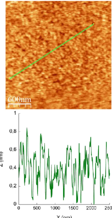
Ge N2+ 3-N2 Ge 4-Ge 4-Si H H Si H H Si H H+ e -Nstretch from 0.5 nm to 1 nm, depending on the conformation of the butyl chains. A global thickness between 2.6 and 3.2 nm is thus expected, assuming that the terminal phenyl group of the organic tether is linked to the Si(100) surface with an upright configuration.40 A longer immersion time led to a bilayer, as discussed below (see also Fig. S8; ESI). AFM was used to probe the aspect of the POM film at the nanometer scale and to support ellipsometry measurements: the 2.9 nm sample appears homogeneous on a large zone with a RMS roughness of 0.38 nm (RMS roughness of a Si-H substrate is 0.17 nm, see Fig. S3 and S4; ESI).
The rinsing step is also a key parameter to obtain films of controlled thickness. To optimize it, the sample was characterized by CV just after immersion. A three-electrode cell setup was used with the modified silicon wafer as the working electrode in a pure electrolyte solution. An intense irreversible wave at -0.5 V vs SCE, which corresponds to the reduction of the diazonium function, is observed on the CV recorded at the scan rate of 0.1 V.s-1 (Fig. S1a; ESI). This means that free POM-N2
+
molecules are physisorbed on the substrate, close to the silicon surface. To get rid of these species, the sample was thoroughly rinsed with an abundant flow of ACN, followed by 1 min sonication in an ACN bath. On the CV recorded after rinsing, the diazonium reduction wave has disappeared, proving the effectiveness of the rinsing (Fig. S1b; ESI). The characteristic waves of the two successive oneelectron reduction processes attributed to the POMs are identified at 1.0 and -1.4 V vs SCE (Fig. S1b; ESI) but they are not well defined and appear irreversible. This phenomenon is well known in electrochemistry using silicon electrodes and has been reported several times for different redox couples.41-43 It is explained by the passivation of the silicon electrode by SiO2 formation induced, particularly, by OH- traces. In the present case, such
passivation is systematically observed when CV is recorded down to the potential of the solvent reduction (-1.8 V vs SCE), which may be at the origin of the species responsible for the final Si contamination. The shape of the first wave can be improved by restricting the potential range from 0 to -1.35 V (see below).
The effect of the rinsing step is confirmed by AFM and ellipsometry: after rinsing, the global thickness of the sample decreases to 2.7 nm, with a smaller standard deviation (0.1 nm), which is in agreement with a smoother film, and the AFM images show a flatter sample, with a RMS roughness equal to 0.17 nm (Fig. 1).
X-Ray Photoelectron Spectroscopy was used to characterize the POM layer. The survey spectrum reveals the presence of W, Ge, P, C, N and O elements, confirming the presence of the hybrid POMs on the substrate. High-resolution XPS spectra in the W4f binding energy range display the spin orbit doublet at 36 and 38.1 eV corresponding to W4f7/2 and W4f5/2,
respectively (Fig. 2A). These values are in agreement with the presence of oxidized W(VI) species, as reported for other immobilized polyoxotungstates.11, 44-47 It is confirmed by the presence of a peak at 531.2 eV on the deconvoluted O1s photopeak, which corresponds to oxygen atoms bonded to metallic atoms (Fig. S5; ESI). The Ge2p3/2 peak is centred at
1220.1 eV, in agreement with the Ge-O bonds (1217 eV is tabulated for metallic Ge) (Fig. 2B). The P2p peak was not analysed in this study because it displays a large peak, probably broadened by the presence of an excess of TBAPF6, coming
from the last step of the POM-N2+ synthesis12 (Fig. S5; ESI), and shake-up satellites of silicon atoms. N1s and C1s
photopeaks attest for the presence of the organic tether and the TBA counter cations (Fig. 2C,D). On the C1s spectrum, the aliphatic, the unsaturated and the Ge linked carbon atoms are at the origin of the peak at 285.1 eV, whereas the one at 286.5 eV is characteristic of carbon atoms linked to an ammonium group. The presence of the TBA cations is also attested by the ammonium contribution at 402.4 eV on the N1s peak. The origin of the peak at 400.6 eV on this photopeak is still unclear. Several interpretations are discussed in the ESI and it is most probably due to the anchoring of activated acetonitrile molecules on the silicon surface, which further generate amine groups.48-50 On the Si2p peak, SiO2 contamination is observed
(Fig. S5; ESI). However, for spectrometer availability reasons, XPS measurements were performed about one month after the sample preparation. The POM layer being intrinsically porous due to the steric hindrance of each POM (1 nm in diameter) grafted on the substrate, a slow dioxygen diffusion through the film is allowed and SiO2 is formed after a long standing time,
even in an Ar purged pill-box.
B
A
A
1217 1218 1219 1220 1221 1222 1223 1224 1225 Ge2p 3/2Binding Energy (eV)
B
C
D
C
D
C
B
A
Fig. 2: High resolution X-ray Photoelectron spectra for W 4f, Ge 2p3/2, C 1s and N 1s in a POM monolayer.
To sum up, a flat and homogeneous POM monolayer was prepared by the spontaneous grafting of diazonium post-functionalized POMs. This material is suitable to study the electron transfer properties of the film, therefore vertical and lateral conductivities were probed by CV and SECM respectively.
Cyclic Voltammetry Characterization
Kinetic analysis of the charge transfer from the silicon substrate to the POM monolayer was studied by analyzing the voltammetric response at different scan rates. Cyclic voltammetry was performed using the same procedure as described above, but from 0 to -1.35 V vs SCE (instead of 0 to -1.8 V vs SCE), to permit the study on the first one-electron reduction wave of the POMs while limiting the silicon passivation. A well-defined, reversible and stable wave was obtained and several CVs were recorded at different scan rates (Fig. 3A,B and S2; ESI). The quality of the CV proves that the possible contamination by SiO2 is low on a fresh sample, which attests for the efficiency of the grafting procedure under a controlled
atmosphere. At low scan rates, the one-electron reduction wave is centred at E° = -0.95 V vs SCE (Ep = 59 mV at v = 0.01
V.s-1), a value similar to those reported for these hybrids in solution and grafted on a glassy carbon electrode.12 It is worth noting here the absence of the irreversible wave at -0.5 V vs SCE, showing that there are no diazonium groups near the electrode surface. Moreover, the variation of the intensity is negligible from the first to the third cycle recorded at 0.1 V.s-1, proving that very few species are physisorbed on the modified substrate11 (Fig. S2; ESI) and thus confirming the efficiency of the rinsing described above.
A
Fig. 3 CV of a POMs-modified silicon electrode (~0.35 cm2) in a 0.1 M solution of TBABr in ACN. Scan rates (A) v = 0.01, 0.03, 0.1 and 0.3 V.s-1 ; (B) v = 0.1, 0.3, 1, 3 and 10 V.s-1. (C) Ep,red and Ep,ox variations vs v () and theoretical variations ()
for an electron transfer rate constant kETvert = 5 0.5 s-1.
The wave current was integrated to estimate the grafting layer density. The amount of charge Q transferred in a single step is about 3.4 C. An approximate value for the area A of the immersed modified silicon electrode was measured to be 0.35 cm2, which gives a grafted POM surface concentration of Г = Q/nFA = 9.9 x 10⁻¹¹ mol.cm-2. This value is close to the theoretical value for a compact monolayer, Г = 9.2 x 10⁻¹¹ mol.cm-2, estimated from the POM-to-POM distance in the crystal structure of the reduced TBA4[PW12O40].51 This result strengthens the ellipsometry and AFM conclusions and confirms the formation of
a compact monolayer. To probe the electron transfer performances of the POM layer, we recorded the CV of the modified electrode at different scan rates. The difference between the anodic and cathodic peak potentials, Ep, increases from v > 0.1
V.s-1, indicating kinetic limitations from low scan rates. The peak potential, Ep, analysis of the CVs recorded until 3 V.s-1
(symbols in Fig 3C) are then confronted to the Laviron’s procedure52 (lines in Fig 3C) originally developed to model electron transfer kinetics at metallic electrodes. This method permits, for metallic-like electrodes to extract the electron transfer rate constant, kETvert, owing to the theoretical variations of Ep,red and Ep,ox with v (Fig. 3C). It has to be noted that the
experimental and theoretical curves split up at a scan rate above 1 V.s-1 for the anodic part. This is also observed on the CV: from 1 V.s-1, the anodic wave, situated at a potential above -0.8 V vs SCE, gets broader and smaller whereas the cathodic
peak feature is not modified. A possible explanation is that from this scan rate, the anodic peak potential is above the silicon flatband potential, and that under such depletion conditions, silicon gets less conductive. The flatband potential is thus estimated at -0.8 V vs SCE, which agrees with the values reported in the literature for n-type Si(100) silicon substrates.43, 53, 54 The behaviour of the Si surface in the anodic potential range is then not metallic and Laviron’s procedure cannot apply without taking into account possible surface state contribution which requires the description of the charge carriers potential-distribution. As it requires a deeper knowledge of the band structure and charge carriers density of the Si electrode used, we have disregarded the anodic branch behaviour at high scan rate for kinetic analysis. Except for this behaviour at high scan rate for the anodic part, the theoretical curves fit well with the experimental measurement in the cathodic potential region. The fact that the CV at low scan rates is similar to that of POM grafted on metallic electrode suggests that the Si electrode has a metallic character in potential region more negative than the POM standard potential. The increase of the scan rates is accompanied by a shift of the POM reduction towards more negative potential values. First it reinforces the assumption that the Si electrode has a metallic-character throughout the whole scan rates explored. Then, at the highest scan rates, the Ep,cat
-1,2 -1,1 -1 -0,9 -0,8 -0,7 -0,6 0,01 0,1 1 10 E / V v s E C S v / V.s-1
B
C
values are in the limiting case of irreversible reduction (no consideration of reoxidation of the reduced POM layer). It is then legitimate to use, as was previously done in different examples,38 the methods developed for metallic electrodes to extract a rate constant for the overall charge transfer process. Here, the kinetics of the reduction of the POM layer attached to the Si electrode is thus obtained from the Laviron’s procedure and a kETvert value of 5 s
-1
is deduced. This value is of the same order of magnitude as the one measured by Tour and coll. for hybrid Lindqvist-type POMs (kETvert = 25 s-1).38 The slightly
lower value recorded here can be explained by the different link between the tether and the lacunary POM, a germanium atom rather than an imido group, which could disrupt the conduction way. This value is also directly comparable to the kETvert
value determined for the same POM layer grafted on glassy carbon and reported in a precedent work (kETvert = 800 s -1
). The nature of the surface has thus a strong influence on kETvert. It seems to be specific to this POM system since similar kETvert
values for porphyrin monolayers have been reported on gold and silicon.26, 27 This low kETvert value could be explained by the
presence of SiO2 traces, formed in spite of the conservation precautions. The quantity of SiO2 would be small enough to keep
the silicon electrode conducting while slowing down the electronic transfer. A difference in the grafted layer organization between flat silicon and rough glassy carbon could also bring an explanation. This point is still unclear and will be studied in a following work.
SECM Characterization
Scanning Electrochemical Microscopy in the feedback mode33-37 appears to be an efficient tool for studying redox active molecules immobilized on various substrates either as monolayer or multilayers films,19, 21, 33-37, 55 including silicon substrates.17, 18, 42, 43 Consequently, SECM was used here to probe the charge transfer efficiency within the POM monolayer covalently attached to the Si substrate. Electron transfer kinetics at these modified surfaces was analysed by SECM at a not connected Si substrate (unbiased conditions) using two redox mediators, namely 3-ortho-nitroxylene (3NX) and tetracyanoquinodimethane (TCNQ), the redox potentials of which surround the one of the POM layer, as shown in Scheme 2A. 3NX was chosen as redox mediator because its redox potential (-1.24 vs SCE in DMF) is between the first and the second wave of the POMs reduction (-1.1 V and -1.5 V vs SCE in DMF respectively). Therefore, if the mediator is able to reduce the POM layer (case of 3NX) and if the layer is conducting, the negative charges are transferred through the conducting layer and the mediator is regenerated at the tip. If one of both conditions is not achieved (using TCNQ), the mediator cannot be regenerated at the tip (Scheme 2B).
A
Scheme 2 (A) Redox mediators / layers and their corresponding potentials evaluated in DMF solution containing 0.1M NBu4BF4. (B) Principle of SECM measurements on a POM layer in the case of a) a conducting layer b) an insulating layer.
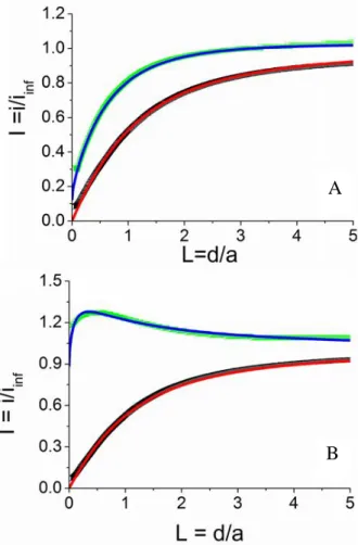
SECM approach curves were first recorded at the unmodified negatively doped Si substrate (n-Si). The principle of the approach curves is detailed in the experimental section. The approach curves obtained using TCNQ and 3NX as redox mediators are shown in Fig. 4A. For TCNQ, the normalized current I recorded at the Pt UME tip decreases with its distance to the n-Si surface, reflecting the absence of regeneration of the oxidized form of the mediator at the interface (negative feedback).33 This approach curve is in good agreement with the theoretical variation expected for an insulating substrate (red line). If 3NX is used as a redox mediator, a feedback is observed, which means that 3NX- is partially oxidized at the bare n-Si substrate. This behaviour suggests that at this low potential, the conduction band of Si is reached. However, in the previous work from Fabre et al,43 a pure negative feedback was observed on a n-Si substrate, even when using 9,10-diethoxyanthracene for which the redox potential is -2.29 V vs ECS. This difference can be explained by the presence of a native SiO2 layer on the n-Si substrate (rather than an organic protective layer43), which can shift the conduction band
potential toward more positive values.56,57 This is consistent with the different charge transfer dimensionless constant values extracted from the theoretical fitting curve, observed on different n-Si samples (0.05 to 0.13, Fig. S6). The radius of the microelectrode used (3 μm in ref 43 vs 25 μm herein) can also be a reason for this observation since smaller effects are detected with larger UME radii (κ = kela/D). Thus, for κ = 0.13 which is the maximum value observed here, it would be κ =
0.016 using a 3 µm radius. This low value would result in an apparent insulating behavior.
Fig. 4 SECM approach curves recorded at a bare Si substrate (A) and at a Si substrate modified by a POM monolayer (B) with a 25 μm radius Pt microelectrode in a solution of DMF containing 0,1 M NBu4BF4 and 4mM TCNQ (□) or 3NX (□).
A
Lines are the theoretical curves using an electrode with Rg =8. (A) Insulating behaviour (red line), = 0.13 (blue line). (B) Insulating behaviour (red line), = 1.1 (blue line).
In a second time, approach curves with TCNQ and 3NX were recorded at a POM grafted n-Si substrate (Fig. 4B). With TCNQ, the approach curve presents exactly the same negative feedback as for the bare n-Si substrate. Indeed, TCNQ°- being generated at a positive potential (E°=0.3 V vs SCE in DMF), it is not able to reduce efficiently the grafted POMs (1st reduction wave at -1.1 V vs SCE in DMF). Instead, the anion radical generated by reduction of 3NX at a more negative potential (E°= -1.24 V vs SCE) than that of the POMs, should be able to inject electrons to the POM layer. Indeed, an increase of the feedback at low L values is observed, reflecting the regeneration of the 3NX mediator due to the POM layer reduction as well as the electron transfer across the POM layer. Theoretical fitting led to a value of 1.1. It is worth noting that reproducible approach curves were obtained on different zones of the POM layer, confirming the great homogeneity of the layer and proving the reliability of the measurements (Fig. S7A; ESI).
For comparison, the charge transfer efficiency was investigated on a grafted POM bilayer. Such a surface was prepared by immersing the n-Si sample into the POM-diazonium solution for 5 h leading to a homogeneous 5.5 nm thick film, as attested by ellipsometry, AFM and electrochemical measurements (Fig. S8; ESI). Such a thickness corresponds to the height of two POM layers. The second layer is most likely made of physisorbed POMs, since a long sonication of the sample in DMF leads to the desorption of the supplementary layer. Moreover, as postulated in a precedent work,12 the covalent attack of the phenyl groups in the organic tether by the diazonium species is probably prevented by the strong hindrance of the POM spheres and its counter-cations on top of the layer. Approach curves recorded at various spots of the bilayer modified surface present an inhomogeneous feedback with a variation of the constant from 0.2 to 0.6 (Fig. S7B; ESI), attesting to an inhomogeneous charge transfer efficiency along the surface. The repartition of the physisorbed POMs on the surface is probably irregular. The maximum value for the constant, = 0.6, which is significantly lower than the one estimated for a monolayer ( = 1.1), demonstrates the importance of the organization of the POM layer to promote an efficient lateral electron conductivity. This observation is consistent with the work on ferrocene anchoring onto a polyphenylene film, which leads to a disorganized layer associated to a lower charge transfer efficiency55 compared to a well-organized monolayer of ferrocene.18
When successive approach curves are recorded exactly on the same spot, a progressive decrease of the feedback current is observed for both the monolayer and the bilayer. It is important to note that this decrease is due to the presence of the POM layer on the substrate since no decrease of the feedback current is observed at the unmodified n-Si Substrate. As shown in Fig. 5, in the case of a monolayer, the constant decreases from 1.1 for the first approach curve to 0.3 for the third one.
Fig. 5 SECM approach curves recorded at a Si substrate modified by a POM monolayer with a 25 μm radius Pt microelectrode in a DMF solution containing 0,1 M NBu4BF4 and 4 mM of 3NX. (A) Successive approach curves at the
same spot of the surface. (B) Successive approach curves recorded after local regeneration of the surface, using Fc+ as redox probe generated at the UME in the vicinity of the interface. Lines are the theoretical curves using an electrode with Rg =8. (A) 1st approach curve = 1.1 (red line), 2nd approach curve = 0.8 (blue line), 3rd approach curve κ = 0.3 (pink line). (B) 1st
approach curve κ = 0.8 (red line), 2nd approach curve κ = 0.2 (blue line).
This can be explained by a progressive degradation of the POM layer or the slow accumulation of negative charges inside the layer, as POMs are known for their ability to trap charges.22, 28 Similar decrease of SECM feedback activity has already been observed in the study of thin organic layers and attributed, based on theoretical modeling, to charge accumulation or saturation in the layer.58, 59 The CVs presented in Fig. 3 support the latter explanation since they show a difficult oxidation of the POM- layer, suggesting a limited injection of electrons from the layer to the Si substrate, maybe due to the proximity of the flatband potential of the Si substrate. If the negative charges are trapped by the POMs, the use of an oxidative agent should facilitate their evacuation. Thus, in an attempt to regenerate the surface, ferrocene (E°=0.45 V vs SCE in DMF) was added to the solution and oxidized at the UME tip at the vicinity of the electrode for 100 s after the third approach curve presented in Fig. 5A. Approach curves were then recorded again using 3NX, as shown in Fig. 5B. The first approach curve shows a recovering of the feedback fitting with a theoretical constant = 0.8, which corresponds to the constant given by the second approach curve in Fig. 5A. The second approach curve recorded at the same point shows a decrease of the feedback, proving that it is again possible to store a negative charge within the POM layer. All these observations strongly suggest the possibility to accumulate negative charges in the POM layer. It is interesting to mention that if the surface is left in the solution of 3NX for about 10 min, no recovering of the feedback is observed. Thus, an efficient discharge of the POM layer is only possible using an oxidative species with a potential higher than that of the layer. The ability of the surface to trap charges in the POM layer could be very valuable for many applications such as electronic memories.
A
Conclusions
The elaboration of a dense and homogeneous monolayer of hybrid POMs on silicon constitutes one step forward in the study of the integration of POMs into memory devices. Key experimental parameters are studied to control the thickness and the density of the layer and the sample is thoroughly characterized by surface characterization techniques. Electrochemical measurements are used to study the electron transfer kinetics of the POM layer. A low vertical electron transfer constant (kETvert=5 0.5 s-1) is estimated whereas a good conductivity is measured through the POM layer. Such measurements are a
preliminary step since they probe the solid-liquid interface, which can differ from the solid-solid interface in the memory device configuration. Nevertheless, they give important data, tendencies and issues on the behaviour of the grafted POMs, which will be useful for the studies at the solid state. In particular, a strong substrate effect is observed when moving from glassy carbon to silicon. If the origin of the slow down of the electron transfer with silicon were traces of silicon oxide, making first a dense protecting self-assembled organic monolayer and grafting POMs in a second step could improve the system. This will require a perfect control on the quality of the first organic layer and of the post-functionalization reactions of the POMs applied to surfaces and not in solution, which has been scarcely tested until now. Extensive work is in progress on that purpose. Another important effect regarding the organization of the POM layer was detected by electrochemical measurements. A good organization of the POMs in the layer is crucial, not only to get reliable physical results, but also to promote the POM-to-POM electron transfer. Moreover, progressive and reversible trapping of negative charges inside the layer was observed. Silicon substrates functionalized by a POM monolayer as described here are thus good candidates to be investigated at the solid state, particularly to evaluate their electronic memory properties.
Acknowledgements
Pr Jean Pinson is warmly acknowledged for his relevant advices on the grafting of diazonium compounds and for fruitful discussions throughout this work especially about the interpretation of the N1s photopeak observed by XPS. The authors also thank Dr. Ludovic Tortech for the recording of the AFM images.
Notes and references
a Sorbonne Universités, UPMC Univ. Paris 06, UMR CNRS 8232, Institut Parisien de Chimie Moléculaire, Université Pierre et Marie Curie,
4 place Jussieu, case courrier 42, F-75005 Paris Cedex 05, France. E-mail : anna.proust@upmc.fr
b Sorbonne Paris Cité, Univ. Paris Diderot, ITODYS, UMR CNRS 7086, 15 rue J. A. Baif, F-75013 Paris, France. E-mail :
frederic.kanoufi@univ-paris-diderot.fr
Electronic Supplementary Information (ESI) available: [synthesis of the POM hybrid, additional AFM images, cyclic voltammograms and complementary SECM measurements carried out on a POM bilayer. A thorough discussion about the interpretation of the N1s photopeak is also presented]. See DOI: 10.1039/b000000x/
1 E. C. P. Smits, S. G. J. Mathijssen, P. A. van Hal, S. Setayesh, T. C. T. Geuns, K. A. H. A. Mutsaers, E. Cantatore, H. J. Wondergem, O. Werzer, R. Resel, M. Kemerink, S. Kirchmeyer, A. M. Muzafarov, S. A. Ponomarenko, B. de Boer, P. W. M. Blom and D. M. de Leeuw, Nature, 2008, 455, 956.
2 M. Bouvet, H. Xiong and V. Parra, Sensors and Actuators B: Chemical, 2010, 145, 501.
3 Y. Liu, B. Wolfrum, M. Hüske, A. Offenhäusser, E. Wang and D. Mayer, Angew. Chem., Int. Ed., 2013, 52, 4029. 4 Y. Shirota and H. Kageyama, Chem. Rev. (Washington, DC, U. S.), 2007, 107, 953.
5 M. T. Pope, Comprehensive Coordination Chemistry, Mc Cleverty, J. A. Meyer, T. J. Elsevier Ltd, Oxford, 2004. 6 D. M. Way, A. M. Bond and A. G. Wedd, Inorg. Chem., 1997, 36, 2826.
7 M. Takamoto, T. Ueda and S. Himeno, J. Electroanal. Chem., 2002, 521, 136.
8 N. Fay, A. M. Bond, C. Baffert, J. F. Boas, J. R. Pilbrow, D.-L. Long and L. Cronin, Inorg. Chem., 2007, 46, 3502. 9 M. Sadakane and E. Steckhan, Chem. Rev. (Washington, DC, U. S.), 1998, 98, 219.
10 B. Keita and L. Nadjo, J. Mol. Catal. A: Chem., 2007, 262, 190.
12 C. Rinfray, G. Izzet, J. Pinson, S. G. Derouich, J. J. Ganem, C. Combellas, F. Kanoufi and A. Proust, Chemistry-a European Journal, 2013, 19, 13838.
13 T. He, J. L. He, M. Lu, B. Chen, H. Pang, W. F. Reus, W. M. Nolte, D. P. Nackashi, P. D. Franzon and J. M. Tour, J. Am. Chem. Soc., 2006, 128, 14537.
14 A. M. Douvas, E. Makarona, N. Glezos, P. Argitis, J. A. Mielczarski and E. Mielczarski, ACS Nano, 2008, 2, 733. 15 G. V. Dubacheva, M. Devynck, G. Raffy, L. Hirsch, A. Del Guerzo and D. M. Bassani, Small, 2014, 10, 454.
16 B. L. M. Hendriksen, F. Martin, Y. B. Qi, C. Mauldin, N. Vukmirovic, J. F. Ren, H. Wormeester, A. J. Katan, V. Altoe, S. Aloni, J. M. J. Frechet, L. W. Wang and M. Salmeron, Nano Lett., 2011, 11, 4107.
17 F. Hauquier, J. Ghilane, B. Fabre and P. Hapiot, J. Am. Chem. Soc., 2008, 130, 2748.
18 D. Zigah, C. Herrier, L. Scheres, M. Giesbers, B. Fabre, P. Hapiot and H. Zuilhof, Angew. Chem., Int. Ed., 2010, 49, 3157. 19 Y. Leroux, D. Schaming, L. Ruhlmann and P. Hapiot, Langmuir, 2010, 26, 14983.
20 A. P. O'mullane, J. V. Macpherson, P. R. Unwin, J. Cervera-Montesinos, J. A. Manzanares, F. Frehill and J. G. Vos, J. Phys. Chem. B, 2004, 108, 7219.
21 A. F. Wang, C. Ornelas, D. Astruc and P. Hapiot, J. Am. Chem. Soc., 2009, 131, 6652.
22 C. Busche, L. Vila-Nadal, J. Yan, H. N. Miras, D.-L. Long, V. P. Georgiev, A. Asenov, R. H. Pedersen, N. Gadegaard, M. M. Mirza, D. J. Paul, J. M. Poblet and L. Cronin, Nature, 2014, 515, 545.
23 B. Fabre, Acc. Chem. Res., 2010, 43, 1509.
24 K. Huang, F. Duclairoir, T. Pro, J. Buckley, G. Marchand, E. Martinez, J. C. Marchon, B. De Salvo, G. Delapierre and F. Vinet,
Chemphyschem, 2009, 10, 963.
25 J. S. Lindsey and D. F. Bocian, Acc. Chem. Res., 2011, 44, 638.
26 A. A. Yasseri, D. Syomin, R. S. Loewe, J. S. Lindsey, F. Zaera and D. F. Bocian, J. Am. Chem. Soc., 2004, 126, 15603. 27 K. M. Roth, D. T. Gryko, C. Clausen, J. Z. Li, J. S. Lindsey, W. G. Kuhr and D. F. Bocian, J. Phys. Chem. B, 2002, 106, 8639. 28 A. Proust, B. Matt, R. Villanneau, G. Guillemot, P. Gouzerh and G. Izzet, Chem. Soc. Rev., 2012, 41, 7605.
29 B. Matt, X. Xiang, A. L. Kaledin, N. N. Han, J. Moussa, H. Amouri, S. Alves, C. L. Hill, T. Q. Lian, D. G. Musaev, G. Izzet and A. Proust, Chemical Science, 2013, 4, 1737.
30 R. Villanneau, A. Marzouk, Y. Wang, A. Ben Djamaa, G. Laugel, A. Proust and F. Launay, Inorg. Chem., 2013, 52, 2958. 31 C. Rinfray, S. Renaudineau, G. Izzet and A. Proust, Chem Commun, 2014, 50, 8575.
32 B. V. Zeghbroek, Principle of conductor devices, http://ecee.colorado.edu/~bart/book/contents.htm. 33 M. V. M. A. J. Bard, Scanning Electrochemical Microscopy, Taylor & Francis, New York, 2012. 34 S. Amemiya, A. J. Bard, F.-R. F. Fan, M. V. Mirkin and P. R. Unwin, Annu. Rev. Anal. Chem., 2008, 1, 95. 35 G. Wittstock, M. Burchardt, S. E. Pust, Y. Shen and C. Zhao, Angew. Chem., Int. Ed., 2007, 46, 1584. 36 R. Cornut and C. Lefrou, J. Electroanal. Chem., 2007, 608, 59.
37 R. Cornut and C. Lefrou, J. Electroanal. Chem., 2008, 621, 178.
38 M. Lu, W. A. Nolte, T. He, D. A. Corley and J. M. Tour, Chem. Mater., 2009, 21, 442.
39 M. P. Stewart, F. Maya, D. V. Kosynkin, S. M. Dirk, J. J. Stapleton, C. L. McGuiness, D. L. Allara and J. M. Tour, J. Am. Chem. Soc., 2004, 126, 370.
40 D. E. Jiang, B. G. Sumpter and S. Dai, J. Am. Chem. Soc., 2006, 128, 6030. 41 J. N. Chazalviel and T. B. Truong, J. Am. Chem. Soc., 1981, 103, 7447.
42 B. Fabre, D. M. Bassani, C. K. Liang, S. Lhenry and P. Hapiot, J. Phys. Chem. C, 2013, 117, 12725. 43 B. Fabre, D. M. Bassani, C. K. Liang, D. Ray, F. Hui and P. Hapiot, J. Phys. Chem. C, 2011, 115, 14786. 44 B. Fleury, M. Billon, F. Duclairoir, L. Dubois, A. Fanton and G. Bidan, Thin Solid Films, 2011, 519, 3732.
45 R. J. Errington, S. S. Petkar, B. R. Horrocks, A. Houlton, L. H. Lie and S. N. Patole, Angew. Chem., Int. Ed., 2005, 44, 1254. 46 D. Mercier, S. Boujday, C. Annabi, R. Villanneau, C. M. Pradier and A. Proust, J. Phys. Chem. C, 2012, 116, 13217. 47 N. Legagneux, J. M. Basset, A. Thomas, F. Lefebvre, A. Goguet, J. Sa and C. Hardacre, Dalton Trans., 2009, 2235. 48 P. Doppelt, G. Hallais, J. Pinson, F. Podvorica and S. Verneyre, Chem. Mater., 2007, 19, 4570.
49 A. Berisha, C. Combellas, F. Kanoufi, J. Pinson, S. Ustaze and F. I. Podvorica, Chem. Mater., 2010, 22, 2962. 50 A. Berisha, C. Combellas, G. Hallais, F. Kanoufi, J. Pinson and F. I. Podvorica, Chem. Mater., 2011, 23, 3449.
51 W. L. Huang, L. Todaro, G. P. A. Yap, R. Beer, L. C. Francesconi and T. Polenova, J. Am. Chem. Soc., 2004, 126, 11564. 52 E. Laviron, J. Electroanal. Chem., 1979, 101, 19.
53 D. Laser and A. J. Bard, J. Phys. Chem., 1976, 80, 459.
54 H. Z. Yu, R. Boukherroub, S. Morin and D. D. M. Wayner, Electrochem. Commun., 2000, 2, 562. 55 D. Zigah, J.-M. Noël, C. Lagrost and P. Hapiot, The Journal of Physical Chemistry C, 2010, 114, 3075. 56 D. C. Gleason-Rohrer, B. S. Brunschwig and N. S. Lewis, J. Phys. Chem. C, 2013, 117, 18031. 57 O. Seitz, T. Bocking, A. Salomon, J. J. Gooding and D. Cahen, Langmuir, 2006, 22, 6915. 58 C. Combellas, F. Kanoufi, D. Mazouzi, J Phys Chem B 2004, 108, 19260-19268.