A Distributed Software Architecture for
Semiconductor Process Design
by
Matthew D. Verminski
B.S. in Computer Engineering, Tufts University (1996)
Submitted to the Department of Electrical Engineering and Computer Science in partial fulfillment of the requirements for the degree of
Master of Science in Electrical Engineering and Computer Science
at theMASSACHUSETTS INSTITUTE OF TECHNOLOGY
February 1998
© 1998 Massachusetts Institute of Technology All rights reserved.
/
Signature of Author:Certified by:
Certified by:
Department Af Electrical Engineering and Computer Science January 15, 1998
Michael B. McIlrath Research Scientist, Electrical Engineering and Computer Science Thesis Supervisor
/ Donald E. Troxel
Professor of Electrical Engineering and Computer Science
, -- Thesis Supervisor
Accepted by:
Chairman, Department
Arthur C. Smith Committee on Graduate Theses
A Distributed Software Architecture for
Semiconductor Process Design
by
Matthew D. Verminski
Submitted to the Department of Electrical Engineering and Computer Science in partial fulfillment of the requirements for the degree of
Master of Science in Electrical Engineering and Computer Science
at the
MASSACHUSETTS INSTITUTE OF TECHNOLOGY
Abstract
Computer representations for semiconductor fabrication processes are currently not well defined for distributed computing. This work focuses on defining and implementing an open, distributed software architecture for designing semiconductor fabrication processes. The implementation of the architecture provides a common interface to semiconductor process repositories, a life cycle service to manage the distributed objects, various means for organizing distributed repositories, and clear component definitions to enable a trader to find and manage available services. The base interfaces and services are essential in the development of distributed and shared applications for semiconductor process design.
Thesis Supervisor: Title:
Thesis Supervisor: Title:
Michael B. McIlrath
Research Scientist, Electrical Engineering and Computer Science Donald E. Troxel
Acknowledgments
There are many people who have provided me with feedback, help, and support during the past year and a half of research. I cannot possibly thank them all, but I will try.
I would like to thank Professor Donald Troxel for providing me with the research
assistantship that has funded my education at MIT. He has provided valuable feedback and insight as an advisor. I would also like to thank Michael McIlrath for providing a research topic and guiding me to its completion. Our weekly meetings kept the project on schedule and were the source of many critical ideas. William Moyne has shown the patient and courage necessary to program the first application with the software
architecture. I would like to thank him for his help with the semiconductor process browser and the numerous poster sessions. Myron "Fletch" Freeman was instrumental in
helping me recover from a few system crashes along the way.
I would like to thank my officemates, Yonald Chery, Manuel Perez, Brian Lee, Erik
Pedersen, Jared Cottrell, Thomas Lohman, and Francis Doughty, for providing a friendly and innovative environment in which to work.
Many friends allowed me to balance my research and class work with outside activities. Brian Herrick, Justin Steele, Aaron Bradshaw, Christopher Centurelli, and Thomas Lampron ensured that I had breaths of real air and social interaction. Coach Don Megerle continues to be an unending source of advice and friendship. I have been
incredibly fortunate to have so much emotional support from my mom, my dad, and my brother, Brian.
My work has been made possible by the support from the Defense Advanced
Table of Contents
1 INTRODUCTION ... .... 8
1.1 R ELA TED W O RK ... ... 8
1 .1 .1 F A B L E ... 9
1.1.2 Process Design Aid (PDA)... 10
1.1.3 Berkeley Process Flow Language (BPFL)... 11
1.1.4 Process Flow Representation (PFR)... ... 11
1.1.5 Semiconductor Process Representation (SPR) Information Model ... 12
1.2 D ISTRIBUTED SYSTEM S ... 13
1.2.1 Common Object Request Broker Architecture (CORBA) ... 13
1.2.2 SEMATECH CIM Framework... . ... 15
1.3 THESIS STATEMENT ... 17
1.4 O RGANIZATION OF THESIS ... 17
2 SYSTEM ARCHITECTURE ... 18
2.1 IDL FOR SEMICONDUCTOR PROCESS REPRESENTATION (SPR) ... 19
2.2 LIFE CYCLE SERVICE ... 20
2.3 REPOSITORY ORGANIZATION ... ... 21
2.4 TRADER SERVICE ... 22
2.5 APPLICATIONS ... ... ... 23
3 SEMICONDUCTOR PROCESS REPRESENTATION ... 25
3.1 O V ERV IEW ... 25
3.2 DESCRIPTION... ... ... 25
3.3 INTERFACES ... 26
3.3.1 Base D ata Structures ... ... .. ... 27
3.3.2 B ase O bjects ... ... 28
3.3.3 Processes & Views... ... ... 29
3.3.4 Process View ... .. ... 30 3.3.5 Effects ... .. ... 30 3.3.6 Equipment View ... 34 3.3.7 Environment View... 34 3.4 SERVER IM PLEMENTATION... ... ... 35 3.5 PERSISTENT STORAGE ... 37
3.6 EXAMPLE CLIENT INTERACTIONS ... ... ... 37
4 LIFE CYCLE SERVICE ... 39
4 .1 O V ERV IEW ... 39
4.2 D ESCRIPTION... ... 39
4.2.1 Factories... ... ... 39
4.2.2 Locating Factories... 40
4.3 INTERFACES ... 40
4.3.1 B ase Structures ... ... 40
4.3.2 G eneric Factory... ... ... 41
4.3.3 Factory Finder... ... ... 42
4.3.4 Life Cycle Object ... 42
4.4 IMPLEMENTATIONS ... 43
4.4.1 Generic Factory... 43
4.4.2 Factory Finder... ... ... 45
4.4.3 Life Cycle Object ... 45
4.5 E XAM PLES ... 45
5 ORGANIZING AND SEARCHING THE REPOSITORY ... 48
5.1 O V ERV IEW ... 48 5.2 LIBRARY SERVICE... 48 5.2.1 D escription ... .. ... 48 5.2.2 Interfaces ... ... ... 49 5.2.3 Im p lem entation ... 50 5.2.4 Example ... .. ... 50 5.3 Q UERY EXTENSIONS ... ... 51 5.3.1 D escription ... .. ... 51 5.3.2 Interface ... . ... 52... 5.3.3 Implementation ... ... .. ... ... ... . 52 5.3.4 E xam p le ... ... 53 6 LOCATING SERVICES ... ... 54 6.1 O VERV IEW ... 54 6 .2 D ESC R IPTIO N ... 54 6.3 SERVICE T YPES ... 56 6.3.1 SPR Repository ... ... ... 56 6.3.2 SP R L ibrary ... ... 56 6.3.3 Factory Finder... ... ... 57 6.4 E XAM PLES ... 57
7 SEMICONDUCTOR PROCESS BROWSER ... 61
7.1 O VERV IEW ... 6 1 7.2 FINDING SERVICES ... ... .61
7.3 LIBRARY SERVICE ... .. ... ... 62
7.4 SPR SERVICE ... 63
7.5 UTILIZING THE LIFE CYCLE SERVICE... ... ... 64
8 CO N CLU SIO N ... 65
R EFER EN C ES ... 67
APPENDIX A - SPR IDL ... ... 69
APPENDIX B - SPR ODL ... 76
APPENDIX C - LIFE CYCLE IDL ... 82
APPENDIX D - CATALOG IDL ... 85
List of Figures
Figure 1: Semiconductor process design cycle ... 9
Figure 2: FABLE process layers ... 10
Figure 3: PFR layer abstractions ... 11
Figure 4: CA FE architecture ... ... 12
Figure 5: Object Management Architecture... 15
Figure 6: C IM fram ew ork ... ... 16
Figure 7: Distributed software architecture for semiconductor process design ... 18
Figure 8: SPR server development... ... 20
Figure 9: SPR view s ... ... 20
Figure 10: Life cycle service interacting with SPR service ... 21
Figure 11: Library service indexing repository... ... 22
Figure 12: A trader interacting with services ... ... 22
Figure 13: Selecting a simulator using the trader service. ... 23
Figure 14: Selecting a remote fabrication service using the trader service ... 23
Figure 15: Process step divided into multiple views ... .... .26
Figure 16: D eposit effect... ... 32
Figure 17: Conformal deposit effect ... 32
Figure 18: Planar deposit effect ... 32
Figure 19: CORBA skeleton and stub interaction... ... 36
Figure 20: SPR Java implementation hierarchy ... ... 36
Figure 21: Persistent SPR classes... 37
Figure 22: Client and factory interaction ... ... 40
Figure 23: Factory finder interface used in conjunction with other location services ... 40
Figure 24: Client creating a process object ... ... 44
Figure 25: L ibrary service ... ... 49
Figure 26: Adding service types... 58
Figure 27: Query with constraints ... 60
Figure 28: Q uery w ith preference ... 60
Figure 29: Browser interacting with trader service ... ... 62
Figure 30: Browser interacting with library service... ... 63
List of Tables
Table 1: Base SPR data structures... 28
Table 2: Foundation SPR interface objects ... ... 29
Table 3: Generic view and process interfaces ... ... 30
Table 4: Process view interface ... 30
Table 5: Effects view interface...31
Table 6: Simple effect location data structure... ... 31
Table 7: Effect specific parameter interfaces ... ... 31
T able 8: E ffects interfaces ... ... 33
Table 9: Equipm ent view interface ... 34
Table 10: Machine and equipment interfaces ... ... 34
Table 11: Environment view interface ... ... 35
Table 12: Basic environment interfaces ... ... 35
Table 13: Simple client navigation of a semiconductor process ... 38
Table 14: Basic life cycle data structures ... ... 41
Table 15: Generic factory interface... 42
Table 16: Factory finder interface ... 42
Table 17: Life cycle object interface ... 43
Table 18: Life cycle client example ... 46
Table 19: Life cycle client with helper class ... ... 47
Table 20: Output of client interaction ... 47
Table 21: Catalog data structure... 49
T able 22: Library interface... ... 50
Table 23: Library exam ple ... 51
Table 24: Output of library example... 51
Table 25: Q uery data structures ... 52
Table 26: Query capable factory interface ... ... 52
Table 27: Q uery extensions exam ple ... 53
Table 28: Exam ple service type ... 55
Table 29: Repository service definition ... ... 56
Table 30: Library service definition... 57
Table 31: Factory finder service definition ... ... 57
Table 32: Service offer for SPR Library ... 58
Chapter 1
Introduction
Building integrated circuits requires semiconductor fabrication processes. Current software systems for designing these fabrication processes are not built for distributed computing. This research implements and evaluates a distributed, platform independent software architecture for semiconductor process design. The architecture provides well-defined application programming interfaces for process repositories and surrounding services. To automate common network programming tasks, the interfaces use the Object Management Group's (OMG) Common Object Request Broker Architecture (CORBA).
This chapter begins by providing an introduction to previous work done in the area of semiconductor process representation. Next, distributed systems are discussed. A thesis statement follows this. The chapter concludes by presenting the organization of the thesis.
1.1 Related Work
A semiconductor process is affected and influenced by numerous steps during its life
cycle from origination to fabrication and maintenance. New processes generally emanate from evolutionary changes to existing processes or the creation of new technologies. An example of an evolutionary change occurs when improved equipment is used. The introduction of a new technology, e.g. Silicon Germanium, might require creating an entirely new fabrication process.
When a new process is designed, the description can begin as a desired performance parameter specification. A process is then generated and simulated to satisfy the given constraint, adding specific information such as machine settings, environments, and effects to describe the process. An integrated circuit is then fabricated to collect data on actual performance characteristics of the process. The results are cycled back through each stage until the performance characteristics are finalized (see Figure 1).
Circuit Designer
Fabrication
Process Designer Figure 1: Semiconductor process design cycle
The design cycle for a semiconductor process demonstrates the need for an
information model to communicate process information. The structure must encompass data that is viewed differently depending upon its position in the cycle. A variety of Technology Computer Aided Design (TCAD) tools and Computer-Aided Manufacturing
(CIM) systems have been researched and designed to address this issue. The following
sections outline several of these systems.
1.1.1 FABLE
Stanford University's FABLE was the first attempt to develop a structured representation for semiconductor processes [1]. The project generated a procedural language for
representing processes. The language was highly structured with multiple abstraction levels for modeling semiconductor fabrication processes.
FABLE programs represent process steps with hierarchical layers. The five layers
the highest level of abstraction, provides a general description of a process step (e.g. etch-oxide). The effect layer details any operation on the wafer (e.g. what and where is the oxide etched). The treatment layer corresponds to the specific operations needed to obtain the desired wafer state (e.g. how the oxide is etched). The settings layer describes the specific equipment needed for the step and its corresponding settings. Finally, the
physical layer details the processing of the wafer.
Process
Effects
Treatment
Settings
Physical
Figure 2: FABLE process layers
The FABLE project was not successful due to several limitations. The detailed structure proved very restrictive and not useable in a real manufacturing environment [2]. The language was not extensible and could not keep pace with rapidly evolving process technology. Lastly, FABLE was not able to interface to applications other than
manufacturing.
1.1.2 Process Design Aid (PDA)
Building on the FABLE research, Stanford generated a second representation for
semiconductor processes as part of the Process Design Aid (PDA) project [3]. An object-oriented process representation was coupled with PDA. It divided processes into a hierarchical structure where each process step was a class. The process step was
constructed from the base class or inherited from it with additional attributes. The PDA process representation was flexible and extensible. This proved to be advantageous in that a user was free to add any attributes desired, and detrimental in that it was possible for some process descriptions to not be interpreted correctly by applications. Unlike FABLE, PDA interfaced well with simulators but lacked robust manufacturing support.
1.1.3 Berkeley Process Flow Language (BPFL)
The Berkeley Process Flow Language (BPFL) [2] was developed during the same time as PDA. BPFL was a programming-language-based approach for representing
semiconductor processes. It represented semiconductor process information with a multiple view structure. For example, specific instructions for performing a process were in a fabrication view while a simulation description was in the simulation view. Other views included equipment and material. A wafer state model with standard control and processing instructions were also defined.
BPFL proved to be effective in a manufacturing environment due to its exception handling and systematic abstraction for process steps. Since BPFL did not provide extensibility, it became difficult to maintain the process representation.
1.1.4 Process Flow Representation (PFR)
As part of the Computer Aided Fabrication Environment (CAFE) at MIT, the Process Flow Representation (PFR) was developed [4]. PFR provides a representation for semiconductor processes. It follows FABLE by abstracting representation layers for processes. PFR uses a three level abstraction model. The change-wafer-state layer describes changes the semiconductor wafer undergoes during an operation. The
treatment layer describes the physical environment surrounding the wafer during the
changes. The settings layer details parameters for the equipment used to achieve the
treatment (see Figure 3).
Settings
Treatment
Wafer State
Figure 3: PFR layer abstractions
In addition, PFR supports unification of process data [4]. This allows for the association of multiple descriptions of processes. For example, a process simulator such
as SUPREM-III [5] uses a specific format for input files. PFR unifies its internal view of the process with external views such as simulator input files.
PFR coupled with the overall CAFE architecture [6], provides a system for
communicating process information between engineers, designers, and manufacturers of semiconductors (see Figure 4). However, the repository is limited to a specific hardware and software platform. This makes it difficult to share information with other
repositories.
Applications
(Scheduling, process design, equipment, data, people, etc.)
Data and Tool Integration Architecture
(PIF, PFR, programmatic interfaces, etc.)
Infrastructure Architecture
(Ingres DB with Gestalt layer, fabform, Unix OS)
Figure 4: CAFE architecture
1.1.5 Semiconductor Process Representation (SPR) Information Model
There are other proprietary, commercial implementations in addition to the models detailed in the previous sections. Semiconductor representations are unique to specific
laboratories and companies making it difficult to transfer process information between
facilities. The varying models for semiconductor processing are not well suited for communicating information between repositories. Researchers at MIT and elsewhere in the TCAD/CIM community have addressed the need for a common representation of
semiconductor processes by developing the Semiconductor Process Representation Information Model (SPR) [7].
SPR organizes process information into different views. The four main views are
effects, environment, equipment, and sub-processes. The equipment view contains
information about the machines for a process step. During the fabrication, the equipment produces a particular environment around a wafer, which in turn causes the effects on a wafer [7]. Sub-processes provide structure for dividing process information amongst multiple smaller steps.
A common interface to access semiconductor process repositories is essential for process designers to share and exchange information between repositories. The SPR information model incorporates the strengths of proven systems, in addition to addressing the weakness of previous models by providing extensible components for structured growth and expansion. The SPR information model can be used for exchanging
information about processes within a distributed software architecture for semiconductor process design.
1.2 Distributed Systems
Software for designing semiconductor processes (e.g., process simulation, editing, and synthesis) is currently programmed for specific software and hardware platforms.
Platform interoperability is essential for a distributed software architecture to incorporate legacy systems. The system should be able to integrate existing applications and reuse available services.
A distributed, platform independent software architecture provides numerous benefits for semiconductor processing research. Process designers can choose between any simulator, editor, or synthesis tool without being restricted by a particular operating system and hardware platform. Semiconductor fabrication benefits from the distributed software architecture. Due to expenses associated with fabricating semiconductors, lack of state-of-the-art equipment often limits research facilities. A distributed software
architecture facilitates the sharing of remote resources and equipment.
1.2.1 Common Object Request Broker Architecture (CORBA)
The Object Management Architecture (OMA) is a consortium specification created by the Object Management Group (OMG). Including over 700 company members, the
object-oriented distributed computing [8]. The OMA's core is the Common Object Request Broker Architecture (CORBA). It provides interoperability among a variety of hardware and software platforms. CORBA defines an "Interface Definition Language (IDL) and Application Programming Interfaces (API) that enable client/server object interaction within implementations of Object Request Brokers (ORB)" [8]. In essence, CORBA is a technology that readily allows the development of distributed systems.
In addition to CORBA, the OMA consists of interfaces and functional specifications for common services and facilities (see Figure 5). These are defined as CORBA services and CORBA facilities. CORBA services focus on common object services for managing a distributed system [9]. Included are specifications for naming, event handling,
persistent objects, life cycles, trader, querying, etc. CORBA facilities are of two types
-domain (vertical) and common (horizontal) [10]. Domain facilities concentrate on specific vertical domains such as manufacturing, healthcare, telecommunications, and finance. Common facilities provide application functionality such as user interfaces, help facilities, and document management. The benefits of software reuse and interoperability is realized by using agreed upon standard interfaces for services. Applications utilizing the common interfaces are allowed to choose services between providers implementing the functionality.
To automate common networking programming tasks, programming interfaces for the distributed software architecture for semiconductor process design utilize CORBA. Furthermore, the architecture employs reusable CORBA services when appropriate.
Application Interfaces Vertical (Domain) CORBAfacilities HealhCare Manufacturing Enance Horizontal (Common) CORBAfacilities UserInterfaces Help Facility Do cument Management
Object Request Broker (ORB)
Figure 5: Object Management Architecture
1.2.2 SEMATECH CIM Framework
The OMG is focused on defining specifications for the common object services and facilities that are applicable to generic distributed systems. Industry consortia, such as
SEMATECH, are left to generate interfaces for domain-specific facilities. SEMATECH,
a consortium of U.S. semiconductor manufactures, works with government and academia to sponsor and conduct research in the area of semiconductor manufacturing. A CORBA based CIM framework is currently being developed by SEMATECH for semiconductor manufacturing. The CIM Framework is a vertical CORBA facility within the OMA (see Figure 5).
The objective of the SEMATECH CIM Framework is to provide a software
infrastructure for integrating applications and sharing information for the manufacturing of semiconductors. The framework's intent is to establish an open industry standard for creating semiconductor CIM systems [11].
Object Services (CORBAservices)
The CIM Framework defines the following component modules for managing a semiconductor manufacturing system [12]:
* Factory management * Document management * Labor management * Machine management * Material management
* Process definition management * Process specification management * Schedule management
The modules provide a basis for CIM applications such as process tracking, machine control, etc (see Figure 6).
CIM Applications WIP Tracking Process Control
process control,
work-in-Machine
Control ...
Object Request Broker (ORB)
Factory Document Labor
Management Management Management
c o m m o n Iu
Components Machine Process
Management Management
Figure 6: CIM framework
The focus of the CIM framework is to provide the appropriate manufacturing abstractions and services for the semiconductor industry. The scope of the framework encompasses all aspects of semiconductor manufacturing from billing and shipping to machine management. Within the framework, there is a need to communicate
information about semiconductor processes. The current framework [12] has allocated components for process definition and specification management. Final component
definitions have not yet been specified by SEMATECH. One intent of the research presented in this paper is to develop a process design representation that can be used in conjunction with the SEMATECH CIM framework.
1.3 Thesis Statement
Current computer representations for semiconductor processes are not well defined for distributed computing. Hardware and software dependencies, varied protocols for inter-communicating, and undefined interfaces for managing distributed data are several weaknesses of existing representations. The research presented in this thesis focuses on defining and implementing a distributed software architecture for designing
semiconductor processes. The architecture addresses the need for a common
representation for processes and implements surrounding services for managing the system based upon industry standards. The implementation of the services is done in Java [13] to provide platform independent components that can be used as the foundation for further distributed system development.
1.4 Organization of Thesis
This chapter has served to provide a brief background on current systems used for semiconductor process design. In addition, an overview of distributed systems was discussed. Finally, the problems and challenges of defining a distributed framework for semiconductor process design were presented.
In the following chapter, an overview of the entire system is presented. Then, Chapters 3 through 6 discuss the details of specific modules by exploring their interfaces and implementations. Applications that utilize the architecture are detailed in Chapter 7. Finally, Chapter 8 summarizes the thesis and details areas for further research.
Chapter 2
System Architecture
The distributed software architecture for semiconductor processing provides reusable, inter-operable services (see Figure 7). The architecture adheres to the philosophy of CORBA by using standard OMG interfaces for common object services such as life cycle and trader [14]. The combination of core services provides an architecture for distributed semiconductor process design.
The SPR service is the basis for accessing process information in the distributed software architecture. It utilizes a generic information model for describing
semiconductor processes. Joining SPR are three supporting services for organizing and managing the distributed process objects. The life cycle service provides interfaces for creating, copying, moving, and removing the distributed objects. Extensions to the life
cycle service enable querying process databases. A library service provides a common
interface for organizing collections of processes. Lastly, a trader is used to find and manage available services.
In parallel with the implementation of the distributed software architecture, a semiconductor process browser was developed. The process browser application demonstrates aspects of the architecture implementation. It allows a user to view processes in distributed repositories. The process browser interacts with the four main services. It uses the trader service to connect to a library service. The life cycle service can be integrated for managing the creation and movement of the distributed objects.
Once the browser has access to repositories, it uses the SPR interface to access information about processes.
2.1 IDL for Semiconductor Process Representation (SPR)
The SPR information model provides a standard medium for communicating information about fabrication processes [7]. It combines the needs of process designers (TCAD) and manufacturers (CIM). These characteristics make it suitable for defining the
programming interfaces for a distributed software architecture for semiconductor process design. The SPR programming interfaces are defined in CORBA IDL and are used to access existing as well as new process repositories. The use of a standard interface allows process designers and manufacturers to integrate services and applications via a standard communications mechanism.
The implementation of the SPR programming interface consisted of three phases (see Figure 8). The first defined the IDL based upon the SPR information model document [7]. The second phase implemented the server in Java for developing and refining the interface definitions. After establishing the interfaces, the third phase created a persistent storage backend.
Phase 3 Persistent storage backend
with PSE for Java
Figure 8: SPR server development
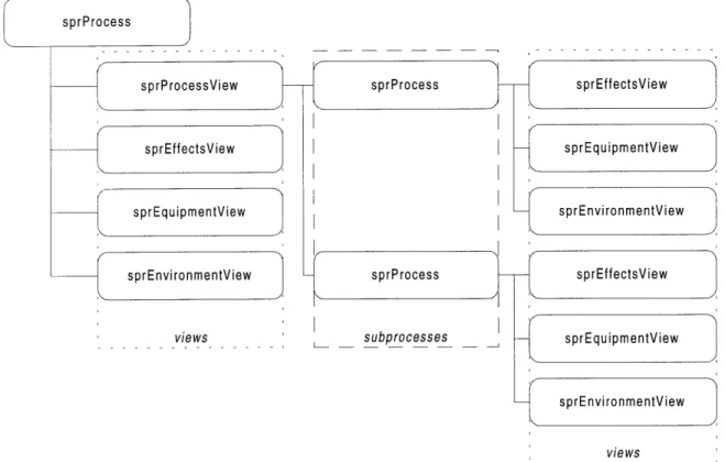
The server implementations closely reflect the SPR information model. The model provides an organized representation for process information. SPR organizes process information into four main views - effects, environment, equipment, and process (see
Figure 9). The process view is a division of a process into sub-processes. The other views (effects, environment and equipment) describe what occurs during the process. The
equipment for a process creates an environment that causes the effects [7].
sprView
sprProcessView sprEffectsView sprEquipmentView sprEnvironmentView
Figure 9: SPR views
2.2 Life Cycle Service
The life cycle service provides functionality for creating, deleting, copying, and moving distributed objects. Distributed systems need conventions for clients to manage and perform such operations on remote objects. The implementation of a life cycle service coupled with the SPR service is the core of the SPR repository.
The OMG defined life cycle service consists of three interfaces - a life cycle object, a factory finder, and a generic factory [9]. The base interface is the life cycle object. Object interfaces must inherit from the life cycle object to implement life cycle
functionality. The life cycle object defines operations for copying, moving, and removing an object. Each subclass of the life cycle object implements these methods. The factory
finder interface provides afind factories operation used for obtaining factory references. A single reference to a factory finder interface enables a client to access any factory within its scope. The factory finder is a directory of factories that exist within its scope. The generic factory interface is the base for creating objects. Its create object method uses criteria to produce instances of objects.
There are various issues that are addressed in the life cycle service implementation. For copying and moving, the definition of shallow versus deep is clearly specified (e.g., copying a reference to an object versus copying an object's data). The removal of an object involves complex issues such as distributed garbage collection and dangling references. The life cycle service was developed in tandem with the SPR service (see Figure 10). Furthermore, the Java implementations of these services are coupled with a persistent storage backend.
Semiconductor Process Repository
SPR Service
Client
Life Cycle Service
Figure 10: Life cycle service interacting with SPR service 2.3 Repository Organization
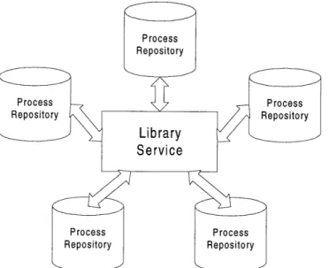
The organization of repositories was defined in a service separate from SPR to allow multiple abstractions and implementations. A library service organizes processes into catalogs. The processes of a catalog can be stored in repositories distributed across multiple systems. The library service organizes a distributed process repository as a single entity (see Figure 11).
Figure 11: Library service indexing repository
For additional repository organization, query extensions were added to the life cycle service. This allows querying to utilize the underlying repository databases. The query extensions provide a generic interface masking the underlying database engine.
2.4 Trader Service
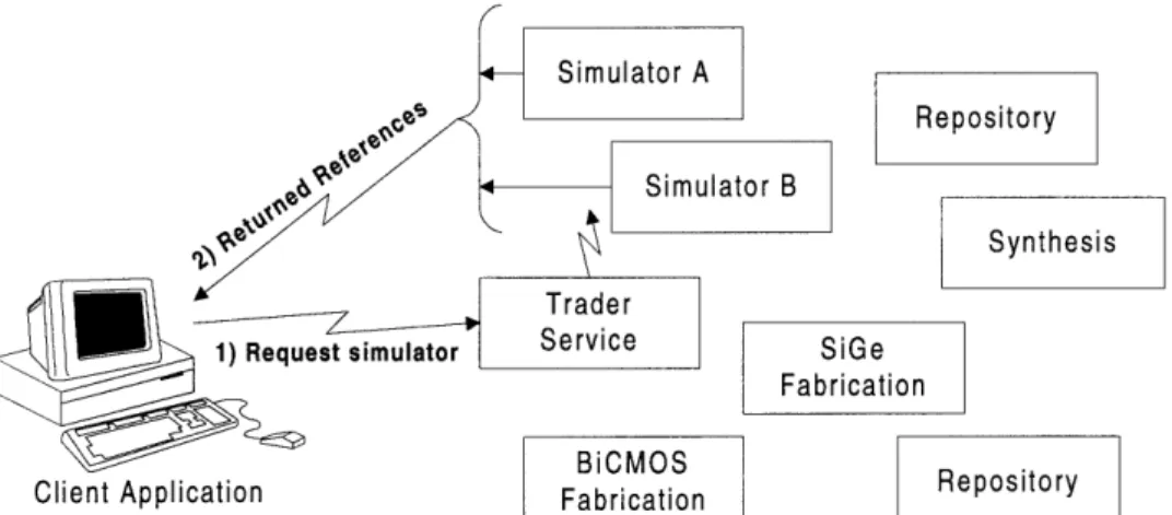
A trader facilitates the exporting and importing of services. A service advertises its
functionality to a trader (exporting). The trader then takes requests from clients and matches the desired functionality with an advertised service (importing). Figure 12 shows the interaction of an advertised service (exporter), a client (importer), and a trader.
3) A link is established between the client and the service by the
trader
The distributed software architecture incorporates a generic trader that client applications use to obtain services. For example, when a client needs a specific simulator, it passes a request to the trader. The trader then returns references to any qualified simulators. The program or user can select a simulator from these references (see Figure 13). Suppose that the client requests a remote fabrication service that uses a BICMOS process. The trader returns references to all the remote fabrication services
that "advertise" a BICMOS process (see Figure 13). Finding a specific simulator or remote fabrication service are two examples of using the trader.
/d
MRepositoryIe
I
Simulator
B
e Synthesis
W
Trader1) Request simulator Service SiGe Fabrication
BiCMOS Repository
Client Application Fabrication Repository
Figure 13: Selecting a simulator using the trader service.
Simulator A
Repository Simulator B
Synthesis
W
Trader1) Request BiCMOS Service SiGe
process Fabrication
fie rnBiCMOS
Client Application eren Fabrication Repository
Figure 14: Selecting a remote fabrication service using the trader service.
2.5 Applications
In order to test and demonstrate the functionality of the distributed software architecture, a semiconductor process browser was developed. The process browser is a comparable
services and machines across a network. The browser uses the distributed software architecture for semiconductor process design as the protocol for interacting with
services. The browser allows a user to view processes. It can also be enabled to support other services such as simulators and fabrication tools as they become available through the trader service.
The browser demonstrates a client application interacting with the SPR, life cycle,
library, and trader services. The trader is the main interface from the browser to the
Chapter 3
Semiconductor Process Representation
3.1 OverviewTo share and distribute information efficiently, a standard data representation is
necessary. The semiconductor process representation (SPR) is intended to provide this standard for communicating information about fabrication processes. Thus, SPR was chosen as the basis for the process information programmatic interfaces within the distributed software architecture. The interfaces are defined in CORBA IDL and are therefore language independent; repositories and clients can be implemented in multiple languages across platforms. The standard interfaces allow process designers and
manufacturers to integrate services and applications seamlessly across global networks.
3.2 Description
The SPR model organizes information into multiple views. The model has four base views - effects, environment, equipment, and process (see Figure 15). In addition,
developers are allowed to use generic or custom views for data unification and extensibility. Views encapsulate specific domain and discipline information about a process. The view abstraction is a mechanism for capturing the diverse information to support both TCAD and CIM applications.
Generally, a process is broken down into smaller stages. The process view provides this abstraction; it divides processes into sub-processes. The other base views depict details of the process. The equipment view contains timing and setting information for
machines. The effects view describes what changes are performed on a wafer. The thermal and chemical environment of the wafer during processing is detailed in the
environment view. Possible custom views include legacy process representations and
simulator specific instructions. The interfaces and components associated with these views are discussed in the following section.
views Figure 15: Process step divided into multiple views.
3.3 Interfaces
The SPR information model is extensible, laying the foundation for describing any semiconductor process. For practical application, SPR cannot possibly account for every process characteristic today and in the future. Thus, the model is extensible to account for growth and change. Extensibility is provided by a foundation of reusable interfaces for managing generic properties. These interfaces are used to construct view specific interfaces to access and organize semiconductor processes.
This section initially details the basic data structures. Then, the generic, reusable interfaces are described. Finally, the base SPR interfaces are illustrated.
3.3.1 Base Data Structures
There are two fundamental approaches for specifying data structures for a distributed environment. Data structures can be defined with the interfaces or strings may be used to pass data types. For the first case, all the information about the structure is tightly
coupled with the interfaces. This guides implementations to adhere to the defined structures. In the latter case, strings must be parsed and unparsed according to an agreed upon specification in order for multiple implementations to operate equivalently. For the SPR implementation, the base structures are coupled with the interfaces to provide explicit definitions.
In addition to standard data types inherent with CORBA IDL, structures are defined for time duration, statistical floating point values, generic values, and units (see Table 1). A structure defines time duration as two integer values for hours and minutes and a floating-point value for seconds. Using a structure to represent time duration is not as extensible as an interface, but is beneficial in that the amount of information transmitted over the network is less. Additionally, the structure provides a restriction on a time duration's units to ensure that they are used equivalently by all applications. A
correlating specification is that any time duration with minutes greater than sixty defines an unspecified value. Interfaces that use a time duration can provide specific methods for converting units of time to the duration structure. The statistical floating-point structure
associates a standard deviation with a value. This is important for specifying process parameters that are digested experimental data or design specifications with tolerances. For specifying generic values, the sprValue union is defined to be either a primitive data
type, a statistical floating-point value, or an sprParameter (defined on page 28). The
sprValue type could have been implemented as a CORBA any type. Any enables the
passing of all IDL defined interfaces and basic types. The sprValue was used instead of any because it provides additional information to implementations. Lastly, an
enumeration is defined for possible units. This currently contains only a few basic units, but can be further expanded when the system has progressed beyond the current
struct sprDuration { long hours; long minutes; float seconds; 1; struct sprStatFloat { float mean; float sdev;
enum sprValueType { BOOLEAN, SHORT, LONG, FLOAT, DOUBLE, STRING,
PARAMETER, STATFLOAT }; union sprValue switch(sprValueType)
case BOOLEAN: boolean Boolean;
case SHORT: short Short;
case LONG: long Long;
case FLOAT: float Float;
case DOUBLE: double Double;
case STRING: string String;
case PARAMETER: sprParameter Parameter;
case STATFLOAT: sprStatFloat StatFloat;
enum sprUnits { NONE, m, mm, nam, pm, sec, ns, ps, cSt, A};
Table 1: Base SPR data structures.
3.3.2 Base Objects
The foundation of the SPR information model defines a set of basic objects which are then used to provide extensibility for objects within the framework. Properties are used
as an extensibility mechanism. A property is a name, value pair. The sprProperty interface is defined with interfaces for setting and retrieving a name and a value (see Table 2). Properties are useful for modeling characteristics that are not otherwise accounted for specifically by an object. Documentation and instructions are possible properties.
Properties alone do not provide extensibility. The sprExtensibleObject furnishes it
by providing interfaces for managing a sequence of properties (see Table 2). This
enables an object based on the sprExtensibleObject interface to contain a set of properties. The property sequence is used to model additional attributes.
Naming an object is a common convention. A name is useful for distinguishing between specific instantiations of objects. The sprNamedObject is an abstract interface used for attaching a name reference (see Table 2). This interface combines with
The last two base interfaces define generic parameters for detailing primitive process
information - sprParameter and sprTimedParameter (see Table 2). A parameter is a value associated with a unit of measure. A timed parameter is a start value and an end
value with corresponding units. Using these basic parameters, constant and time-varying
state information is described.
interface sprProperty : LifeCycle::LifeCycleObject {
void setName(in string inPropertyName);
string getName();
void setValue(in sprValue inValue);
sprValue getValue();
interface sprExtensibleObject : LifeCycle::LifeCycleObject {
void setProperties(in sprPropertySeq inProperties);
void addProperty(in sprProperty inProperty);
sprPropertySeq allProperties();
interface sprNamedObject : LifeCycle::LifeCycleObject {
void setName(in string inObjectName);
string getName();
interface sprExtensibleNamedObject:sprNamedObject,sprExtensibleObject{};
interface sprParameter : LifeCycle::LifeCycleObject {
void setValue(in sprValue inValue)
raises (sprInvalidValue); sprValue getValue();
void setUnits(in sprUnits inUnits)
raises (sprInvalidUnits); sprUnits getUnits();
interface sprTimedParameter : sprParameter {
void setEndValue(in sprValue inEndValue);
sprValue getEndValue();
Table 2: Foundation SPR interface objects
3.3.3 Processes & Views
The sprProcess interface is designed for encapsulating information about a semiconductor process (see Table 3). It is a named container derived from the
sprExtensibleNamedObject interface. In addition to its inherited name and properties, methods are defined for managing the multiple views of a process object. Views are used to associate multiple descriptions with a process design.
The generic view interface, sprView, contains methods for defining and retrieving the view type (see Table 3). The four base views - process, effects, environment, and
equipment inherit from this base interface. Additional views can be defined by extending
this interface. Custom views enable the encapsulation of application specific data. An example is defining a custom simulation view. Defining additional views should be done with caution. The intent of the model is to specify common process information within the base views. A simulation view should only contain the instructions or
transformations necessary for the simulator to use the base SPR views. It is not efficient to have multiple views containing the same process information.
interface sprView : sprExtensibleNamedObject {
void setViewType(in string inViewType);
string getViewType ();
interface sprProcess : sprExtensibleNamedObject {
void setViews(in sprViewSeq inViews)
raises (sprNotUniqueViewType);
void addView(in sprView inView)
raises (sprNotUniqueViewType); sprViewSeq allViews ();
Table 3: Generic view and process interfaces
3.3.4 Process View
The sprProcessView provides structure for subdividing processes (see Table 4). It creates a structure to manage process information enabling the reuse of process objects. For instance, a sub-process for depositing a material only needs to be defined once. Then, multiple process views may reference this process.
interface sprProcessView : sprView {
void setSubProcesses(in sprProcessSeq inSubProcesses);
void appendSubProcess(in sprProcess inSubProcess);
sprProcessSeq allSubProcesses();
Table 4: Process view interface
3.3.5 Effects
Effects represent changes that occur to a wafer. A sequence of effects within the
step (see Table 5). Applicable information within the effects view is often used by wafer state simulators.
interface sprEffectsView : sprView {
void setEffects(in sprEffectSeq inEffects);
void appendEffect(in sprEffect inEffect);
sprEffectSeq allEffects();
Table 5: Effects view interface
A data representation for location is necessary for specifying an effect. The location defines where on a wafer the effect occurs. For the prototype implementation of SPR, a structure was defined for a simple effect location (see Table 6). The simple effect
location contains a string defining a region of material coupled with a boolean specifying whether the region is exposed to the effect. More complex effect locations can be
appended as necessary.
struct sprSimpleEffectLocation ( string MaterialRegion;
boolean IsExposed;
enum sprEffectLocationType {SIMPLE} ;
union sprEffectLocation switch(sprEffectLocationType) case SIMPLE: sprSimpleEffectLocation Simple;
Table 6: Simple effect location data structure
For effects, distance and material are defined as specific parameters (see Table 7). They are used to filter and narrow the broad scope of parameters. A distance parameter's value type is limited to being only a double or a string indicating "all" by the
implementation. sprMaterial is implemented to only accept values of type string.
interface sprDistance : sprParameter { };
interface sprMaterial : sprParameter { };
Table 7: Effect specific parameter interfaces
Effects take a wafer state and transform it to new wafer state. Specific effects
interfaces are defined beyond the base sprEffect in this prototype system (see Table 8). The base effect interface contains a location. The change material effect specifies a change from an old to a new material. The deposit effect describes the coating of a
vertical layer of material (see Figure 16). The conformal and planar deposit effects are subtypes of the deposit effect. The conformal deposit effect deposits a material that assumes the shape of the base layer (see Figure 17). The planar deposit effect deposits a level layer of material (see Figure 18).
Figure 16: Deposit effect
Figure 17: Conformal deposit effect
Figure 18: Planar deposit effect
The vertical etch effect has an interface for a thickness and a material. The thickness is a number or 'all' indicating that all the material should be etched. For a strip etch
effect, the implementation ensures that the thickness is "all." Thus, the entire material
layer is removed. For an isotropic etch effect, an equal thickness of material is removed across the entire wafer. The base interface for the growth effect contains the type of the material grown, the resulting thickness, and the depth consumed from the underlying layer.
interface sprEffect : sprExtensibleObject {
void setEffectLocation(in sprEffectLocation inEffectLocation); sprEffectLocation getEffectLocation();
interface sprChangeMaterialEffect : sprEffect {
void setOldMaterial(in sprMaterial inOldMaterial);
sprMaterial getOldMaterial();
void setNewMaterial(in sprMaterial inNewMaterial);
sprMaterial getNewMaterial();
interface sprDepositEffect : sprEffect {
void setMaterial(in sprMaterial inMaterial);
sprMaterial getMaterial();
void setThickness(in sprDistance inThickness);
sprDistance getThickness();
interface sprConformalDepositEffect : sprDepositEffect { ;
interface sprPlanarDepositEffect : sprDepositEffect { );
interface sprEtchEffect : sprEffect {
void setMaterial(in sprMaterial inMaterial);
sprMaterial getMaterial();
void setThickness(in sprDistance inThickness);
sprDistance getThickness();
interface sprStripEtchEffect : sprEtchEffect { ;
interface sprIsotrophicEtchEffect : sprEtchEffect { };
interface sprGrowthEffect : sprEffect {
void setMaterial(in sprMaterial inMaterial);
sprMaterial getMaterial();
void setThickness(in sprDistance inThickness);
sprDistance getThickness();
void setDepth(in sprDistance inDepth);
sprDistance getDepth();
Table 8: Effects interfaces
More effects such as add field and diffusion can be added to the model. The effects were expanded in detail to support initial applications and testing of the system with process design tools. The method used to extend the SPR IDL with additional effects can
3.3.6 Equipment View
The equipment view defines base interfaces for describing processing equipment. Additional parameters and equipment interfaces or properties can be used to provided
more details about the machines and equipment settings. The equipment view interface contains two methods for describing the equipment setup and operation (see Table 9).
interface sprEquipmentView : sprView {
void setMachines(in sprMachineSeq inMachines);
void appendMachine (in sprMachine inMachine);
sprMachineSeq allMachines ();
void setSettings(in sprEquipmentStateSeq inSettings);
void appendSetting(in sprEquipmentState inSetting);
sprEquipmentStateSeq allStates();
Table 9: Equipment view interface
Equipment specific interfaces include equipment state and machine (see Table 10). The equipment state is a set of properties associated with a duration. The machine is a
named entity with a set of properties. In a thorough SPR implementation, these two
interfaces are the base for a collection of interfaces for fabrication equipment.
interface sprEquipmentState : sprExtensibleObject {
void setTimeDuration(in sprDuration inTimeDuration);
sprDuration getTimeDuration() ;
interface sprMachine : sprExtensibleObject {
void setMachineName(in string inName);
string getMachineName() ;
Table 10: Machine and equipment interfaces
3.3.7 Environment View
The base interfaces are defined for the environment view. The physical state surrounding the wafer is described using a set of environments (see Table 11). Physical-based process simulators customarily utilize the environment view. The view may be created by
collecting fabrication statistics. For example, data such as electron concentration and energy spectra collected from a plasma etcher may be used to create an environment
interface sprEnvironmentView : sprView {
void setEnvironment(in sprEnvironmentSeq inEnvironment);
void appendEnvironment(in sprEnvironment inEnvironment);
sprEnvironmentSeq allEnvironment ();
Table 11: Environment view interface
The environment parameter interface is a specific instance of a timed parameter. It is used to encapsulate models reflecting the state surrounding the wafer. Sets of
environment parameters form the general environment interface (see Table 12).
interface sprEnvironmentParameter : sprTimedParameter { };
interface sprEnvironment : sprExtensibleObject{
void setTimeDuration(in sprDuration inTimeDuration);
sprDuration getTimeDuration() ;
interface sprGeneralEnvironment : sprEnvironment { void setEnvironmentParameters
(in sprEnvironmentParameterSeq inParameters); void appendEnvironmentParameter
(in sprEnvironmentParameter inParameter);
sprEnvironmentParameterSeq allEnvironmentParameters ();
Table 12: Basic environment interfaces
3.4 Server Implementation
CORBA IDL translates into corresponding skeletons and stubs for an assortment of programming languages. Skeletons are code generated for the server-side
implementation of objects. The stubs are code generated to enable client access to the objects. Client and server interaction such as managing network connections and transferring data are performed by skeletons and the stubs (see Figure 19). The SPR server implementation of skeletons was done in Java [13] to provide a platform independent prototype.
Object Stubs
Figure 19: CORBA skeleton and stub interaction
There are two techniques for associating an implementation object with a skeleton -inheritance and delegation [15]. With -inheritance, the implementation object extends the skeleton directly. Delegation associates an implementation object with the skeleton. Java does not support multiple inheritance. Ergo, the inheritance method of an implementation object must inherit directly from the skeleton. Consequently, the delegation method was chosen for implementing the SPR interfaces due to the extensive use of inheritance among the objects. The class hierarchy of the Java implementation
closely follows the inheritance structure of the interfaces (see Figure 20).
Figure 20: SPR Java implementation hierarchy
Object Skeletons
3.5 Persistent Storage
The initial SPR implementations were used for testing and developing the interface definitions. When the base SPR interfaces became finalized, a persistent implementation was created. PSE for Java [16] was employed to create an object-oriented database for the core set of SPR objects with attributes. As shown in Figure 21, the core classes are a subset of the interface hierarchy. An object model was defined (see Appendix D) and implemented in Java for storing process information persistently to disk. Within the defined database classes, methods convert distributed object references to strings for persistent storage.
Figure 21: Persistent SPR classes
The development of the SPR and life cycle services were closely coupled. Chapter 4 details more specifically how the persistent classes interact with the CORBA
implementations.
3.6 Example Client Interactions
The client example presented in Table 13 obtains a process reference, prints its name and the view types it contains. All the object method invocations appear as normal Java calls. The distributed mechanisms operating within this program are hidden to the programmer in the automatically generated stubs. Obtaining an initial reference to a process object has multiple approaches and is discussed with latter services such as the library and
1 sprProcess etchOxide = << obtain initial reference >>;
2 System.out.println(etchOxide.getName() + " process has views of
type:");
3 sprView[] views = etchOxide.allViews();
4 for(int i = 0; i < views.length; i++) {
5 System.out.println(" - " + views[i].getViewType());
6 1
Chapter 4
Life Cycle Service
4.1 OverviewThe OMG life cycle service defines interfaces for creating, deleting, copying, and moving distributed objects [14]. In a distributed environment, operations provided by the life
cycle service allow clients to manage objects in remote locations.
The life cycle service addresses object creation and location. Object creation is a mechanism for creating objects at a remote location. An interface is defined for
producing remote objects. Object location entails how and where clients indicate remote object destinations while preserving the CORBA principal of location transparency. An interface is defined for locating remote objects.
4.2 Description
4.2.1 Factories
A factory is an object that creates and initializes new instances of objects (see Figure 22).
With access to a factory, a client can create multiple objects instances. The factory determines the location of the new object and allocates the necessary resources for its implementation. Resources typically include memory or persistent storage mechanisms.
Application tReference to new object
a new object Create_object F o
Factory
Service Figure 22: Client and factory interaction
4.2.2 Locating Factories
The notion of location is a major concern for any distributed system. Services such as
naming and trader are two services that address this issue. Location is necessary to
create, move, and copy objects. When an object is moved, a mechanism for specifying "where" the object is moving is needed. For the OMG Life Cycle service, the factory
finder interface is used to determine location. The factory finder may be implemented as
a standalone object managing available factories; or, it may be coupled with the organizational power of a naming or trader service (see Figure 23).
FactoryFinder NamingContext FactoryFinder Trader
NamingBasedFactoryFinder TraderBasedFactoryFinder
Figure 23: Factory finder interface used in conjunction with other location services.
4.3 Interfaces
The Life Cycle service consists of three interfaces - generic factory, life cycle object, and factory finder. These interfaces and some base data structures are discussed in the
following subsections.
4.3.1 Base Structures
Three data structures are used with the life cycle service (see Table 14). A Key structure is defined as a name and a hostname. Keys are used to name and locate factories. A
factory entry structure associates a key with a generic factory. Lastly, a name value pair
pass any primitive data type or defined interface. Sequences of the Name Value Pair structure are used to pass Criteria to factories and factory finders.
struct Key { string name; string hostname; struct factory_entry { Key key; GenericFactory factory_ref; typedef struct NVP ( string name; any value; } NameValuePair;
typedef sequence <NameValuePair> Criteria;
Table 14: Basic life cycle data structures
4.3.2 Generic Factory
The job of a generic factory is to match creation criteria specified by clients of the
GenericFactory interface (see Table 15) with specific factory implementations [14].
The OMG defines create_object and supports methods for the GenericFactory interface. The methods list_objects, remove_object, and shutdown are custom extensions.
Create_object is a generic creation method that passes requests to specific factory
implementations. It takes a key to identify the factory implementation and criteria to define how the object is initialized. The supports operation returns true if the generic factory can create an object given a factory key. The list_objects operation takes a key to identify a specific factory and returns a sequence of all the objects created by that specific factory. The remove_object method takes a factory key and object reference and removes the specified object from the factory's list of created objects. It returns true if the
removal is successful. This operation is intended for use with persistent storage mechanisms. The shutdown method is for remotely shutting down a generic factory
interface GenericFactory { boolean supports(in Key k);
Object createobject(in Key k, in Criteria the_criteria) raises (NoFactory, InvalidCriteria, CannotMeetCriteria); ObjectSeq listobjects(in Key k)
raises (NoFactory);
boolean remove_object(in Key factory_key, in Object obj_ref) raises (NoFactory);
void shutdown();
Table 15: Generic factory interface
4.3.3 Factory Finder
Clients use a factory finder interface to specify the destination of a move or a copy operation. The FactoryFinder interface (see Table 16) has one OMG defined method
-findfactories. The methods addfactory and shutdownAll are custom extensions. The findfactories operation takes a key to identify the target generic factory. A
sequence of factories with matching keys is returned by the operation. The addjactory method passes a key and a generic factory reference to be added to the factory finder's scope. The operation is used by generic factory implementations to notify the factory finder of its location. The shutdownAll method shuts down the factory finder service and all the factory objects within its scope.
interface FactoryFinder {
Factories find_factories(in Key factory_key) raises (NoFactory);
void add_factory(in Key factory key, in GenericFactory factory_ref) raises (DuplicateKey);
void shutdownAll();
};
Table 16: Factory finder interface
4.3.4 Life Cycle Object
Objects participate in the life cycle service by extending the LifeCycleObject interface. The OMG defines the copy, move, and remove operations for the LifeCycleObject
interface (see Table 17). The methods getMarker, setFactoryName, and getFactoryName are custom extensions.
The copy operation makes a copy of the object. The factory finder and criteria determine the new object's location. A reference to the new object is returned by the
method. The move operation moves an object to the location specified by the factory finder and criteria. It returns its new reference. The remove method instructs the object to destroy itself. The object reference is no longer valid after the remove operation successfully completes. The get_marker operation returns a string containing the object's interface name. Factories notify an object that the factory created it by using the
setFactoryName method. The getFactoryName operation is used to determine which
factory created the object instance.
interface LifeCycleObject {
LifeCycleObject copy(in FactoryFinder there, in Criteria the_criteria) raises (NoFactory, NotCopyable, InvalidCriteria, CannotMeetCriteria); LifeCycleObject move(in FactoryFinder there, in Criteria the_criteria) raises(NoFactory, NotMovable, InvalidCriteria, CannotMeetCriteria); void remove ()
raises (NotRemovable); string getMarker();
void setFactoryName(in string name);
string getFactoryName();
Table 17: Life cycle object interface
4.4 Implementations
The components of the life cycle service were implemented in Java. The SPR
implementations participate by implementing a defined functionality. In the case of the
life cycle service, this is the life cycle object interface. The generic factory also
participates by passing the task of object creation to object-specific factories. The factory
finder is the only generic aspect of a life cycle service implementation. 4.4.1 Generic Factory
The generic factory object implements operations for support, create_object, list_objects,
remove_object, and shutdown. The generic factory does not perform the actual creation.
Specific implementation factories for individual objects that the generic factory supports perform the creation. For the distributed software architecture for semiconductor process design, the generic factory supports creating all the objects defined by the SPR service (see Chapter 3).
The specific factories for each SPR object extend from an abstract factory class that implements base methods such as listing the objects created and removing objects from this list. The abstract factory persistently stores the list of object references it creates.