HAL Id: hal-01874490
https://hal.laas.fr/hal-01874490
Submitted on 14 Sep 2018
HAL is a multi-disciplinary open access
archive for the deposit and dissemination of
sci-entific research documents, whether they are
pub-lished or not. The documents may come from
teaching and research institutions in France or
abroad, or from public or private research centers.
L’archive ouverte pluridisciplinaire HAL, est
destinée au dépôt et à la diffusion de documents
scientifiques de niveau recherche, publiés ou non,
émanant des établissements d’enseignement et de
recherche français ou étrangers, des laboratoires
publics ou privés.
High-resolution on-chip supercapacitors with ultra-high
scan rate ability
Ty Mai Dinh, Kevin Armstrong, Daniel Guay, David Pech
To cite this version:
Ty Mai Dinh, Kevin Armstrong, Daniel Guay, David Pech. High-resolution on-chip supercapacitors
with ultra-high scan rate ability. Journal of Materials Chemistry A, Royal Society of Chemistry, 2014,
2 (20), pp.7170 - 7174. �10.1039/c4ta00640b�. �hal-01874490�
High-resolution on-chip supercapacitors with
ultra-high scan rate ability
Ty Mai Dinh,
abKevin Armstrong,
cDaniel Guay
cand David Pech*
abA simple approach for the fabrication of high-resolution on-chip supercapacitors with increased performances is demonstrated. The resulting micro-devices display high specific cell capacitance (3 mF cm-2 using hydrous ruthenium
oxide electrode) and impressive scan rate abilities, up to 10 000 V s-1 for multi-walled carbon nanotubes based
micro-supercapacitors, which is five orders of magnitude higher than conventional supercapacitors.
The tremendous push towards systems on chip (SoC) approach together with the decrease of their dimensions has enabled the development of new applications such as wireless sensors network or wearable devices that can be integrated into everyday-use objects. As microelectronic devices get smaller and smaller, it has become critical to power them with micro-power sources of appropriate size, fulfilling specific requirements for self-powered applications such as long lifetime and high-rate charge/discharge capabilities. Electrochemical capacitors (also called supercapacitors) show very interesting characteristics when it comes to these applications, because of their extended lifetimes and high power densities. Supercapacitors store electrical energy using the electrochemical double layer formed at the electrode/electrolyte interface (electrochemical double layer capacitance) or the very fast and reversible electrochemical reaction of some materials deposited at the surface of an electrode (pseudo-capacitance).1,2 The realization
of on-chip micro-sized supercapacitors could satisfy a variety of
micro- power demands and embedded microsystems.3
We have recently shown that the power ability of micro-supercapacitors can be dramatically improved by reducing the physical separation between the anode and the cathode.4,5 Indeed, an
optimized configuration with very high resolution patterns should considerably increase the performances of micro-supercapacitors (capacitance, energy and power normalized to its footprint area on the chip) due to reduced ohmic losses, better impregnation by the electrolyte, higher accessibilities and compactness. However, most of “micro-supercapacitors” reported in literature have resolution above 100 µm, the term “micro” referring mainly to the micro-fabrication techniques used for their micro-fabrication.6-11 Regardless of the
deposition technique, the common challenge is to deposit porous materials on micro-sized substrates without shorting the positive and negative electrodes.12
Here, we demonstrate a new and simple approach for large-scale fabrication of micro-supercapacitors with resolution (i.e. spacing between interdigitated fingers) down to the limit of standard photolithography, i.e. 1 µm (see Fig. S1 in ESI†). The process has been successfully applied for the realization of electric double-layer micro-capacitors (µ-EDLCs) based on multi-walled carbon nanotubes (MWCNTs), and pseudo-capacitive electrochemical micro-capacitors (µ-SCs) based on hydrated ruthenium oxide (hRuO2). The resulting micro-supercapacitors exhibit excellent
electrochemical performances with specific cell capacitance up to 3 mF cm-2 for hRuO
2 and life cycle exceeding 30 000 cycles for
MWCNTs. All micro-devices display also, impressive scan rate abilities, up to 10 000 V s-1 for MWCNTs, which is five orders of
magnitude higher than conventional supercapacitors. The proposed strategy is promising for batch fabrication and integration of operational on-chip micro-supercapacitors into existing micro systems. With electron beam or nano-imprint lithography, the process could also be used for the realization of nano-supercapacitors with sub-micrometer pattern resolutions.
The basic idea for the realization of µ-SCs with high resolution is illustrated in Fig. 1a,b. Current collectors (Ti/Au in this case) were first patterned onto an oxidized silicon wafer and protected by an insulating SU8 masking layer using conventional photolithography techniques. We focused, then, on a lift-off process to realize the micro-devices. This is a widely used method for transferring patterns from resist layers to the material to be structured. In our case, we used this technique to pattern, with high resolution, the current collectors as well as the active material.13 The material deposition
was then facilitated as it occurs at wafer level, which is the key to batch fabrication of functional materials on chips. Most importantly, however, this method avoids the necessity to deposit the electrode material onto micro-sized patterned current collectors – which often leads to deposition on unwanted areas. We validated the process down to 1 µm using two different deposition techniques: the
electrophoretic deposition of MWCNTs and the electrolytic deposition of hRuO2 (see Fig. S2 in ESI†). For practical reasons, the
micro-devices were realized with a 10 µm interspace. For both materials, an adherent layer was obtained with a well-defined pattern, without any short circuit between the electrodes (Fig. 1c,d). The thicknesses, which can be easily modulated by controlling the time used for the electrodeposition of the active layer, were 260 and 100 nm for MWCNTs and hRuO2, respectively. As illustrated in Fig.
2, this process has overcome resolution limits for the integration of active materials into micro-fabrication technologies, with one of the smallest resolution ever to be applied for “micro-supercapacitor” applications.14-17 We have investigated the influence of such
resolutions on the performances of µ-SCs.
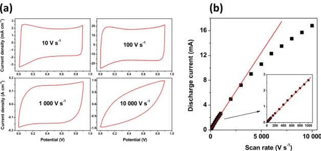
Cyclic voltammograms (CVs) were recorded at scan rates ranging from 0.05 to 10 000 V s-1 in a de-aerated 0.5 M H
2SO4 electrolyte to
evaluate the power capability of the devices. The micro-supercapacitors of both materials display the rectangular shape voltammograms expected for double layer and pseudo-capacitive materials. The symmetrical capacitive behavior was maintained up to an ultrafast scan rate of 10 V s-1 for the hRuO
2-based µ-SC (see
Fig. S3 in ESI†), and to an impressive value of 1 000 V s-1 for the
MWCNTs-based µ-SC (Fig. 3). The MWCNTs micro-sized device was even able to cycle at an ultrafast scan rate of 10 000 V s-1, which
is more than five orders of magnitude higher than conventional supercapacitors, and, to the best of our knowledge, the highest value ever reported for micro-supercapacitors.4,18-21 The specific
capacitances were 0.2 and 3.2 mF cm-2 at 10 V s-1 for the MWCNTs
and the hRuO2-based µ-SCs, respectively. These values are
comparable to the specific capacitances reported in the literature at much lower scan rates for µ-EDLCs (0.4 - 1.5 mF cm-2)22-24 and
pseudo-capacitive µ-SCs (0.4 - 12.6 mF cm-2).5,12,25 The high scan
rate, representative of a high instantaneous power, is thus concomitant with a high specific capacitance. This ability to cycle at such scan rates is due to the very low value of the time constant (τ) of the interdigitated micro-supercapacitors (τ = RC, where ‘C’ is the cell capacitance and ‘R’ is the equivalent series resistance, ESR), thanks to their very high resolution pattern.
To highlight the beneficial effect of the resolution on the power performance, we have simulated the influence of the interspace (i) between the electrodes of planar interdigitated µ-SCs on their time constant (τ), according to the following equation:
! = (%&&+ Ƙ × *+)-
with Rcc the resistance of the current collectors, ρe the resistivity of
the electrolyte and К the analytical expression of the cell constant developed by W. Olthuis et al.5,26
As shown in Fig. 4a, a micro-scale reduction of the interspace between adjacent fingers (of 100 µm width and 1 000 µm length) significantly reduces the contribution of the ESR and consequently, the time constant (τ) is diminished. The corresponding simulations of the CV curves at 1 000 V s-1 for various time constants, according to
the equations developed by B.E. Conway,27 are shown Fig. 4b. We
can clearly see that the CVs of the high resolution micro-supercapacitors can keep a rectangular shape at scan rates (s) exceeding 1 000 V s-1. It is noteworthy that the scan rate ability only
depends on the RC time constant.
Fig. 5a,b shows the Nyquist and Bode plots of the MWCNTs-based µ-SC from 100 kHz to 10 mHz. No leakage current is observed, with the near-vertical straight line (in the low-frequency region) typical of a capacitive material. A negligible equivalent distributed resistance EDR (due to the thin thickness of the active material) and a very low ESR of 0.16 Ω cm2 were estimated from the
high frequency part of the spectrum. As the specific power will predominantly depend on the highest resistive contribution between the ESR and the EDR, the influence of the resolution of the configuration of the micro-device is prominent, in this case, with a maximum specific power of 1.3 W cm-2. Taking into account the
capacitance, the MWCNTs-based µ-SC is characterized by an extremely low time constant (τ) of 32 µs (512 µs for the hRuO2
-based µ-SC, see Fig. S4 in ESI†), which is in complete agreement with the theoretically determined values.
The electrochemical stability of the deposited layers was finally investigated (Fig. 6 and Fig. S5 in ESI†). The capacitance slightly increases after 30 000 cycles at 1 V s-1 for the µ-EDLC, due to a
better electrolyte impregnation with time and cycling.
In conclusion, we have realized high-energy micro-supercapacitors based on hydrated ruthenium oxide, and ultrahigh-power micro-supercapacitors based on multi-walled carbon nanotubes using a simple and integrated-circuits-compatible approach for the deposition of the active material, with extremely high resolutions. This process can be applied to other materials or other deposition techniques. The micro-devices offer truly outstanding performances, with discharge rates of up to 10 000 V s-1.
The use of conventional UV-photolithography techniques (1 µm resolution) currently limits the size of the pattern, but further work will consider using this process with the stepper projection lithography (350 nm resolution) and electron beam lithography (sub-10 nm resolution) for further reduction of the interspace. In turn, these improvements in electrode design should lead to unprecedented performances of micro-supercapacitors.
Acknowledgements
This work was partly supported by the French RENATECH network and financially supported by the French National Research Agency (ANR) through the MIDISTOCK project. T.M. Dinh was supported by a PhD grant and a travel fellowship (ATUPS) from the Université de Toulouse. Collaborations between LAAS and INRS were supported by the Commission Permanente de Coopération Franco-Québécoise (CPCFQ).
Notes and references
a CNRS, LAAS, 7 avenue du colonel Roche, F-31400 Toulouse, France.
Email: dpech@laas.fr; Fax: +33 5 61 33 62 08; Tel: +33 5 61 33 68 37
b Univ de Toulouse, LAAS, F-31400 Toulouse, France.
c INRS-Énergie, Matériaux, Télecommunications, 1650 boulevard Lionel
1 P. Simon and Y. Gogotsi, Nat. Mater., 208, 7, 845-854.
2 S. Chen, W. Xing, J. Duan, X. Hu and S.Z. Qiao, J. Mater. Chem. A, 2013, 1, 2941-2954.
3 M. Beidaghi and Y. Gogosti, Energy Environ. Sci, 2014, 7, 867-884. 4 D. Pech, M. Brunet, H. Durou, P. Huang, V. Mochalin, Y. Gogotsi,
P.L. Taberna and P. Simon, Nat. Nanotechnol., 2010, 5, 651-654. 5 D. Pech, M. Brunet, T.M. Dinh, K. Armstrong, J. Gaudet and D.
Guay, J. Power Sources, 2013, 230, 230-235.
6 K. Wang, W. Zou, B. Quan, A. Yu, H. Wu, P. Jiang and Z. Wei, Adv.
Energy Mater., 2011, 1, 1068-1072.
7 W. Gao, N. Singh, L. Song, Z. Liu, A.L.M. Reddy, L. Ci, R. Vajtai, Q. Zhang, B. Wei and P.M. Ajayan, Nat. Nanotechnol., 2011, 6, 496-500.
8 L. Cao, S. Yang, W. Gao, Z. Liu, Y. Gong, L. Ma, G. Shi, S. Lei, Y. Zhang, S. Zhang, R. Vajtai and P.M. Ajayan, Small, 2013, 9, 2905-2910.
9 M.F. El-Kady and R.B. Kaner, Nat. Comm., 2013, 4, 1475.
10 J. Lin, C. Zhang, Z. Yan, Y. Zhu, Z. Peng, R.H. Hauge, D. Natelson and J.M. Tour, Nano Lett., 2013, 13, 72-78.
11 W. Liu, X. Yan, J. Chen, Y. Feng and Q. Xue, Nanoscale, 2013, 5, 6053-6062.
12 S. Makino, Y. Yamauchi and W. Sugimoto, J. Power Sources, 2013,
227, 153-160.
13 E.T.T Jones, O.M. Chyan and M.S. Wrighton, J. Am. Chem. Soc., 1987, 109, 5526-5528.
14 B. Hsia, M.S. Kim, M. Vincent, C. Carraro and R. Maboudian,
Carbon, 2013, 57, 395-400.
15 M. Beidaghi and C. Wang, Adv. Funct. Mater., 2012, 22, 4501-4510. 16 C. Shen, X.H. Wang, S. Li, J. Wang, W. Zhang and F. Kang, J.
Power Sources, 2013, 234, 302-309.
17 C.H. Chen, D.S.Tsai, W.H. Chung, K.Y. Lee, Y.M. Chen and Y.S. Huang, J. Power Sources, 2012, 205, 510-515.
18 K. Sheng, Y. Sun, C. Li, W. Yuan and G. Shi, Sci. Rep., 2012, 2, 247. 19 A. Ghosh, V.T. Le, J.J. Bae and Y.H. Lee, Sci. Rep., 2013, 3, 2939. 20 Z.-S. Wu, K. Parvez, X. Feng and K. Müllen, Nat. Comm., 2013, 4,
2487.
21 W.-W. Liu, Y.-Q. Feng, X.-B. Yan, J.-T. Chen and Q.-J. Xue, Adv.
Funct. Mater., 2013, 23, 4111.
22 D. Pech, M. Brunet, P.-L. Taberna, P. Simon, N. Fabre, F. Mesnilgrente, V. Conédéra and H. Durou, J. Power Sources, 2010,
195, 1266-1269.
23 P. Huang, M. Heon, D. Pech, M. Brunet, P.-L. Taberna, Y. Gogotsi, S. Lofland, J.D. Hettinger and P. Simon, J. Power Sources, 2013,
225, 240-244.
24 P. Huang, D. Pech, R. Lin, J.K. McDonough, M. Brunet, P.-L. Taberna, Y. Gogotsi and P. Simon, Electrochem. Comm., 2013, 36, 53-56.
25 C.-C. Liu, D.-S. Tsai, D. Susanti, W.-C. Yeh, Y.-S. Huang and F.-J. Liu, Electrochim. Acta, 2010, 55, 5768-5774.
26 W. Olthuis, W. Streekstra and P. Bergveld, Sens. Actuator B, 1995,
24-25, 252-256.
Fig. 1 Micro-supercapacitor fabrication and design. (a) Simplified illustration of the
fabrication process using the lift-off process of the active material for high-resolution pattern
(not to scale). Schematic (b) and optical image (c) of the micro-device. (d) Scanning electron
microscope image of the cross-section of the electrode.
Fig. 2 Comparison of the resolution of state-of-the-art micro-supercapacitors reported in
literature.
Active layer Au Current collectors Active material(a)
(b)
SiO2(c)
(d)
Si Ti 200 µm 200 nm hRuO2electrodeposition Ti/Au deposition Crosslinked photoresist Lift-off Si wafer SiO2layer 10 µm interspace 1000 µm 100 µm 10 µm 1 µmS. Makino et al., J. Power
Sources (2013) [12]
C. Shen et al., J. Power
Sources (2013) [16]
C.H. Chen et al., J. Power
Sources (2012) [17]
M. Beidaghi et al., Adv.
Funct. Mater. (2012) [15]
D. Pech et al., J. Power
Sources (2010) [22]
D. Pech et al., Nat.
Nanotechnol. (2010) [4] M.F. El-Kady et al., Nat. Comm. (2013) [9] L. Cao et al., Small (2013) [8] J. Lin et al., Nano Lett. (2013) [10] W. Gao et al., Nat. Nanotechnol. (2011) [7] W. Liu et al., Nanoscale (2013) [11] K. Wang et al., Adv. Energy Mater. (2011) [6] B. Hsia et al., Carbon (2013) [14] This work To p d own ap pr oac h Obtained resolution
Fig. 3 Cyclic voltammetry charaterizations (CV) of MWCNTs-based micro-supercapacitor.
(a) CVs obtained at different scan rates in de-aerated 0.5M H
2SO
4electrolyte. (b) Evolution
of the discharge current versus scan rate.
Fig. 4 (a) Theoretical evolution of the time constant τ of MWCNTs-based
micro-supercapacitor as a function of the distance between adjacent interdigitated electrodes in 0.5M
H
2SO
4. (b) Calculated cyclic voltammograms expressed as reduced response current (I/sC) at
1
000 V s
-1for various time constant.
0 5 000 10 000 0 4 8 12 16 0 200 400 600 800 1000 0 1 2 3 D isch ar g e cu rr en t (mA ) Scan rate (V s-1) 0.0 0.2 0.4 0.6 0.8 1.0 -3 -2 -1 0 1 2 3 10 000 V s-1 1 000 V s-1 100 V s-1 10 V s-1 Cur ren t d ens ity ( m A c m -2) 0.0 0.2 0.4 0.6 0.8 1.0 -20 -10 0 10 20 0.0 0.2 0.4 0.6 0.8 1.0 -0.2 -0.1 0.0 0.1 0.2 Potential (V) Cur ren t d ens ity ( A c m -2) Potential (V) 0.0 0.2 0.4 0.6 0.8 1.0 -1.0 -0.5 0.0 0.5 1.0
(b)
(a)
200 150 100 50 0 0 10 20 30 40 50 60 70 T ime co n stan t t ( µ s) Interspace (µm) 0.0 0.2 0.4 0.6 0.8 1.0 -1.0 -0.5 0.0 0.5 1.0 t = 500 µs t = 200 µs t = 100 µs t = 50 µs @ 1 000 V s-1 R ed u ced C u rr en t (I /sC ) Potential (V)(a)
(b)
Fig. 5 (a) Nyquist and (b) Bode plots obtained from a MWCNTs-based micro-supercapacitor
in 0.5M H
2SO
4.
Fig. 6 Evolution of the relative capacitance as a function of the number of electrochemical
cycles at 1 V s
-1for a MWCNTs-based micro-supercapacitor (C
0refers to the capacitance
obtained for the first cycle).
0 2000 4000 6000 8000 0 2000 4000 6000 8000 0.0 0.2 0.4 0.6 0.8 0.0 0.2 0.4 0.6 0.8 1 kHz -I m(Z ) ( W cm 2 ) Re(Z) (W cm2) 10 mHz 100 kHz