Publisher’s version / Version de l'éditeur:
Vous avez des questions? Nous pouvons vous aider. Pour communiquer directement avec un auteur, consultez la première page de la revue dans laquelle son article a été publié afin de trouver ses coordonnées. Si vous n’arrivez pas à les repérer, communiquez avec nous à [email protected].
Questions? Contact the NRC Publications Archive team at
[email protected]. If you wish to email the authors directly, please see the first page of the publication for their contact information.
https://publications-cnrc.canada.ca/fra/droits
L’accès à ce site Web et l’utilisation de son contenu sont assujettis aux conditions présentées dans le site LISEZ CES CONDITIONS ATTENTIVEMENT AVANT D’UTILISER CE SITE WEB.
ACS Nano, 14, 3, pp. 2947-2955, 2019-11-27
READ THESE TERMS AND CONDITIONS CAREFULLY BEFORE USING THIS WEBSITE. https://nrc-publications.canada.ca/eng/copyright
NRC Publications Archive Record / Notice des Archives des publications du CNRC :
https://nrc-publications.canada.ca/eng/view/object/?id=9f500ad9-88d4-40d9-a478-38085647dccc https://publications-cnrc.canada.ca/fra/voir/objet/?id=9f500ad9-88d4-40d9-a478-38085647dccc
NRC Publications Archive
Archives des publications du CNRC
This publication could be one of several versions: author’s original, accepted manuscript or the publisher’s version. / La version de cette publication peut être l’une des suivantes : la version prépublication de l’auteur, la version acceptée du manuscrit ou la version de l’éditeur.
For the publisher’s version, please access the DOI link below./ Pour consulter la version de l’éditeur, utilisez le lien DOI ci-dessous.
https://doi.org/10.1021/acsnano.9b07637
Access and use of this website and the material on it are subject to the Terms and Conditions set forth at
Detecting and directing single molecule binding events on H-Si(100)
with application to ultradense data storage
Achal, Roshan; Rashidi, Mohammad; Croshaw, Jeremiah; Huff, Taleana R.;
Wolkow, Robert A.
Detecting and Directing Single Molecule
Binding Events on H‑Si(100) with Application
to Ultradense Data Storage
Roshan Achal,
*
,†,‡Mohammad Rashidi,
†,‡Jeremiah Croshaw,
†,‡Taleana R. Huff,
†,‡and Robert A. Wolkow
†,‡,§†
Department of Physics, University of Alberta, Edmonton, Alberta T6G 2E1, Canada
‡
Quantum Silicon, Inc., Edmonton, Alberta T6G 2M9, Canada
§
Nanotechnology Research Centre, National Research Council of Canada, Edmonton, Alberta T6G 2M9, Canada
*
S Supporting InformationABSTRACT: Many diverse material systems are being explored to enable smaller, more capable and energy efficient devices. These bottom up approaches for atomic and molecular electronics, quantum computation, and data storage all rely on a well-developed understanding of materials at the atomic scale. Here, we report a versatile scanning tunneling microscope (STM) charge character-ization technique, which reduces the influence of the typically perturbative STM tip field, to develop this understanding even further. Using this technique, we can now observe single molecule binding events to atomically
defined reactive sites (fabricated on a hydrogen-terminated silicon surface) through electronic detection. We then developed a simplified error correction tool for automated hydrogen lithography, quickly directing molecular hydrogen binding events using these sites to precisely repassivate surface dangling bonds (without the use of a scanned probe). We additionally incorporated this molecular repassivation technique as the primary rewriting mechanism in ultradense atomic data storage designs (0.88 petabits per in2).
KEYWORDS: atomic-scale memory, controlled chemistry, electronic detection, hydrogen-terminated silicon, scanning tunneling microscope, dangling bond, hydrogen molecule
A
s the end of the current silicon technological roadmap draws closer, ever more capable tools for atomic-scale fabrication are enabling the use of hydrogen-termi-nated silicon as a platform for a number of alternative avenues.1−7The technique known as hydrogen lithography6,8,9(HL) has been used on this surface in the creation of atomic-scale logic elements,5 quantum structures,10 ultradense rewritable memory arrays,6 and controlled chemical reac-tions1,11,12 including the precise placement of dopant atoms.1−3 Using the tip of a scanning probe microscope, single atoms of hydrogen are removed from the surface to create atomically defined dangling bond (DB) patterns. With HL, tailored reactive sites can even be created for specific molecules1,11−15(Supplementary Figure 1). The precise and reproducible spatial integration of molecules into electronic devices is an important consideration toward scalable production, although it remains a considerable challenge. There is a particular focus on the integration of molecules on silicon surfaces to complement and enhance existing technologies.16−20 This is because molecules can exhibit an
array of properties, adding specific functionalities to a given device.16,17,21−24The reactivity of a variety of molecules with
the silicon surface has been studied, including simple molecules like hydrogen13,14 and more complex molecules such as alkenes15,17,20and phosphine.25,26
To propel the spatially controlled integration of molecules with the silicon surface forward, new tools that are capable of uncovering atomic-scale details of single molecule reactions are required. Typical scanning tunneling microscope (STM)-based dynamics studies rely on the observations of the motion and state of molecules, or DB sites, to gain insight into their reactivity. This approach is somewhat limited as the smallest intervals between scans are often many seconds to minutes apart,27,28making real-time observations difficult. There is also the impact of the STM tip as it scans over the area of interest,
Received: September 26, 2019
Accepted: November 8, 2019
Published: November 27, 2019
Article
www.acsnano.org
Cite This:ACS Nano2020, 14, 2947−2955
copying and redistribution of the article or any adaptations for non-commercial purposes.
Downloaded via NATL RESEARCH COUNCIL CANADA on June 22, 2020 at 12:33:06 (UTC).
which can inadvertently deposit material or strongly influence local dynamics through electric field effects and the injection of charge.28−32The latter aspects can additionally complicate the characterization of the amount of charge in DB structures when using only STM measurements, although it is possible to determine the exact charge of defects in some systems through careful analysis and comparison to theory.33,34
Here, we report an all-STM method, which incorporates HL and hydrogen repassivation (HR) techniques6,35,36 to readily characterize the total charge of DB structures at the single electron level, with reduced influence from the STM tip. With this STM method, we were able to reproduce results5,37taken at zero bias with an atomic force microscope (AFM). Once we characterized the number of charges in a given DB structure, such as in an atomically defined reactive site, we then extended this technique to the detection of externally induced charge changes in the DB site and surrounding area. We showed that a single molecule binding event occurring at the DB site can be electronically detected by monitoring for changes in charge. The event can be detected with temporal resolution up to real time, with the possibility of observing multiple bonding events at different DB sites. Combining the ability to precisely create tailored reactive DB sites using HL and the ability to detect a subsequent binding event at those sites provides a framework to study single molecule reactions and to test the reliability of theoretically predicted pathways.38−42
In this work, we also further the prospect of the scalable fabrication of atomic electronics and ultradense room-temper-ature stable memory on hydrogen-terminated silicon. The
recent discovery of HR6,35,36to complement automated HL6 has already resulted in significant fabrication advances,5,6,37 although there is still room to improve repassivation speeds. Currently, the only method to controllably add hydrogen to the surface is to sequentially repassivate DBs with atomic hydrogen attached to a scanned probe.6,35,36When the probe is depleted of hydrogen, it must travel to gather more. By using HL to create specific DB sites, we have demonstrated that we can precisely direct where hydrogen molecules react on the surface of both hydrogen-terminated and deuterium-termi-nated silicon (Supplementary Figure 2) to repassivate DBs without a probe, while leaving other DB structures unreacted. This technique is not only simpler but also faster than HR because it is unencumbered by the finite number of hydrogen atoms that can be adsorbed to a probe,6,35,36 resulting in a more convenient tool to repair fabrication errors in HL. We then integrated this improved repassivation method as the primary rewriting process in a proof-of-concept atomic memory array, with a maximum storage density of 1.36 bits per nm2.
RESULTS AND DISCUSSION
STM Charge Characterization of Atomically Defined Structures.Single DBs on an otherwise hydrogen-passivated silicon surface introduce an isolated electronic state within the silicon band gap.10,31,43 The current through a DB, as measured by an STM tip, can be influenced by the DB’s local electrostatic environment,43,44 including by the charge state of subsurface dopants.43Due to the sample preparation
Figure 1. Characterizing charge occupations (V= −1.6 V, I = 50 pA, T = 4.5 K, 6.4 × 6.4 nm2). (a) STM image of a DB on the hydrogen-passivated Si(100)-2 × 1 surface. The DB (DB1) exhibits a sharp current onset in its I(V) spectrum (f-blue) due to the ionization of a subsurface arsenic dopant atom caused by the STM tip field. (b) A second DB (DB2), containing a net charge of one electron is added to the surface 5.4 nm away from DB1, causing the step in the I(V) spectrum of DB1 to shift to the left (f-dark green). (c) A third DB (DB3) is added near DB2, no shift in the I(V) spectrum of DB1 is observed (f-light green). (d, e) The distance between DB2 and DB3 is varied to determine the net charge in the structure for each case. (f) The I(V) spectra taken over DB1, associated with (a−e), showing the sharp onset of current.
ACS Nano Article
DOI:10.1021/acsnano.9b07637
ACS Nano2020, 14, 2947−2955 2948
method, there is a dopant-depleted region extending over 60 nm from the surface, which largely isolates surface DBs and dopants in this layer from the bulk.45At 4.5 K, dopant atoms laterally separated from the tip by up to 15 nm and at a depth of approximately 5 to 15 nm remain un-ionized (neutral) until a critical tip voltage is reached.43 When one such dopant is field ionized by the tip, the now positive ion core causes downward bending of the local energy bands, thereby creating a conduction channel between the bulk silicon conduction band and the DB level, resulting in a measurable increase of current to the STM tip.43The DB acts as a window into the dopant ionization state, with this sudden onset of current manifesting as a sharp step in its current−voltage, I(V), spectrum43(Figure 1). The step is commonly observed in the
I(V) spectra of most DBs (enabling their use as sensors),
however, the exact strength and critical value of this signature depends on several factors. The sharpness of the tip can alter the value of the critical voltage, as when the tip changes, the strength of its field at the dopant atom changes as well, causing it to ionize at a different critical voltage. The critical voltage also depends on the random proximity of the dopant to the surface and a given DB.43By controllably adding local negative charges on the surface, so as to introduce upward band bending, it is possible to increase the magnitude of the critical voltage where this onset occurs, therefore requiring a larger tip field to achieve dopant ionization. We take advantage of this effect to develop an STM procedure to characterize the amount of net charge in fabricated DB structures (Figure 1a− e). This was previously achieved with sensitive AFM frequency shift measurements of the charge state transitions of a sensor
DB itself,37or by using an AFM to map the spatial localization of charge in DB structures.5
It has been predicted that two closely spaced DBs (<1 nm) on the surface of highly arsenic-doped hydrogen-terminated silicon will share a net charge of one electron, whereas two isolated DBs will have a charge of one electron each.46While recent AFM experiments have verified the single net electron occupation of two closely spaced DBs,5,37 the analogous capability has been lacking in STM. This is principally because the STM applies a large perturbative field while imaging and is capable of injecting or removing charge on the surface. By working with sharp tips (approximately 5 nm radius) at voltages between −1.2 V and −1.6 V and characterizing structures in excess of 5 nm laterally removed from the STM tip, the possible effects of both charge injection and field perturbations can be greatly reduced (seeMethods).
To determine the net charge of a DB structure with an STM, we first recorded a baseline reference I(V) spectrum over a sensor DB (DB1) (Figure 1a,f-blue), which was selected because it exhibited the sharp current onset due to the ionization of a nearby isolated arsenic dopant. We then added a second isolated DB (DB2) 5.4 nm away (Figure 1b), and a new spectrum was taken over DB1. At this distance, AFM experiments performed with zero applied voltage have shown that DB2 will have a net charge of one electron.5,37 In this STM measurement, we observed that the presence of DB2 has increased the critical voltage required to ionize the subsurface dopant, shifting the onset of current observed in the I(V) spectrum of DB1 to a larger negative voltage by −0.06 V (Figure 1f-dark green). The direction of the shift indicates that DB2 is negatively charged. The magnitude of the shift is
Figure 2. Electronically detecting a binding event (V = −1.6 V, I = 50 pA, T = 4.5 K, 11.3 × 7 nm2). (a) STM image taken of the area around a sensor DB exhibiting a sharp current onset in its I(V) spectrum. (b) STM image after the creation of an interdimer site 10.2 nm from the sensor DB. (c) STM image after hydrogen gas was added into the vacuum chamber, and the reaction of a hydrogen molecule with the interdimer site was electronically detected by a shift in the I(V) spectrum taken over the sensor DB. (d) The geometry of the surface, showing the sensor DB (dashed red square), and the location where an interdimer site has been created from DBs (dashed red rectangle) to react with an ambient hydrogen molecule (light blue). (e) The I(V) spectra taken periodically over the sensor DB associated with (a−c).
essentially independent of the distance between the two DBs, as they are not interacting when separated by more than 5 nm,37but rather depends on the distance between DB2 and the dopant atom.43Another DB (DB3) was then added 0.768 nm from DB2 (Figure 1c), and the spectrum of DB1 was measured once more (Figure 1f-light green). The presence of DB3 did not shift the spectrum this time, as would be expected if another negative charge was added into the area, further increasing the critical voltage required to ionize the subsurface dopant. We then erased DB3 using HR and created a new DB 1.15 nm from DB2 (Figure 1d). With this new placement, the spectrum taken over DB1 (Figure 1f-orange) showed an additional shift of −0.065 V, indicating the presence of another charge of one electron in the local area. Repeating this process, DB3 was positioned 1.92 nm from DB2 (Figure 1e), and no additional shift of the I(V) spectrum of DB1 was observed (Figure 1f-red). Since the induced shifts from one and two electrons were very close in magnitude in the I(V) spectrum, we surmise that the un-ionized dopant was sufficiently deep, such that the change in lateral separation of the two DBs in the structure (DB2 and DB3) did not alter their distance to the dopant significantly. Through these STM measurements, we can conclude that 0.768 nm separating DB2 and DB3 gives a net charge of one electron within the pair (due to interelectron repulsion),46while when the spacing is increased to 1.15 nm or more, there is a net charge of two electrons within the structure/local area. These results are in agreement with recent AFM studies5,37 (also see Supplementary Figure 3 for additional AFM results).
Using HL and HR to create and erase a number of isolated DBs (with a charge of one electron) in a particular area, we have demonstrated the capability to calibrate the shifts in the
I(V) spectrum of a sensor DB in order to characterize the
amount of net charge in larger DB structures, with reduced tip field effects. This technique enables minimally perturbative studies of charge occupation using only an STM ( Supple-mentary Figures 4 and 5). In variable-temperature scanned probe systems, we expect it will be possible to observe the I(V) step over a range of temperatures up to approximately 40 K, above which the dopants in the depleted region begin to thermally ionize.47Using this technique, we have determined that two immediately adjacent DBs (as shown in Figure 2), forming an interdimer site, have a net charge of one electron among them (Supplementary Figure 4).
Detection of Single-Molecule Binding Events. Once the amount of charge in a particular reactive site (like the interdimer site) is known, it is possible to use the techniques described above to electronically detect a molecular binding event by periodically recording the I(V) spectrum of a laterally removed sensor DB (or, to achieve greater time resolution, rapidly sampling the current through it at a fixed bias voltage). If there is a change of at least one electron locally when a molecule binds, then there will be an associated change in the
I(V) spectrum (or current). While hydrogen molecules are
generally found to be unreactive toward the clean silicon surface,14,20they are extremely reactive with interdimer sites on an otherwise hydrogen covered surface.14 The sites have zero net charge after hydrogen molecules dissociatively adsorb, repassivating their constituent DBs with hydrogen atoms. This is because the two DB states are eliminated upon each DB reforming a bond with a hydrogen atom.
Previous studies were in disagreement over the preferred pathway (interdimer48 vs intradimer49) for the dissociative
adsorption of hydrogen molecules on the silicon surface. It was eventually shown that the interdimer pathway was the dominant one,13 corroborated by theoretical calculations, which predicted it to be barrierless.38−40,42 These results
relied on sequential STM observations of random adsorption events on the surface.13With HL, instead of observing random events, we created both the inter- and intradimer sites in the same area on the hydrogen-terminated surface. We observed that only the interdimer sites reacted with hydrogen molecules, providing additional, very direct support for the dominance of the interdimer pathway (Supplementary Figure 6).
Figure 2 shows the electronic observation/detection of a single hydrogen molecule binding event to a fabricated interdimer site. To detect the event, we created an interdimer site 10.2 nm (thereby reducing any STM field effects) from a sensor DB exhibiting a sharp onset in its I(V) spectrum (Figure 2a,b,e). We then controllably introduced hydrogen gas (H2) into the vacuum chamber to establish a pressure of 4 ×
10−7 Torr, external to the cryo-shielding, and recorded a
spectrum over the sensor DB at 35 s intervals (seeMethods). After 875 s elapsed, the step in the I(V) spectrum was detected to have shifted back to its original position (Figure 2e), indicating that a binding event occurred, and a hydrogen molecule had dissociatively reacted with the interdimer site. Subsequent imaging of the reaction site confirmed the DBs of the interdimer site had been repassivated with hydrogen (Figure 2c). This technique has the potential to be extended to observe multiple reactive sites, with each site shifting the step of a sensor DB an additional amount (Supplementary Figure 7).
The time for a hydrogen molecule to bind to an interdimer site depends on the pressure of hydrogen gas at the sample surface. Due to the design of the STM chamber, the pressure measurement outside of the cryo-shielding is not an entirely accurate representation of the pressure in the vicinity of the tip and sample, where there is no pressure sensor. There is low flux of gas through the shielding and the cold shield surfaces lower the pressure further through cryo-pumping effects. We believe that the hydrogen molecules are arriving at the interdimer sites from gas phase, as the pressure and temperature of the system are such that H2cannot exist in a
liquid phase.50,51By measuring the reaction time of interdimer sites with hydrogen molecules, the pressure in the vicinity of the sample surface can be estimated (seeMethods).
Directing Single-Molecule Binding Events (Molecular Hydrogen Repassivation). We explored the relative reactivity of hydrogen molecules with a variety of DB structures on both a hydrogen-terminated and deuterium-terminated surface, including with interdimer sites positioned in situations relevant to HL (with different proximities to other DBs and defects) (Supplementary Figures 2a,b and 7a-e). We observed a lack of reactivity of noninterdimer structures with hydrogen molecules (Supplementary Figures 1, 2a,b, and 6). We also did not observe any prohibitive effects on the reactivity of the interdimer sites during our chosen time scales, instead finding them to be highly reactive, even when close to or part of other multi-DB structures. The reactions occurred even while the tip was fully withdrawn from the surface (Supplementary Figure 7). This robust nature and the speed of reaction of hydrogen molecules with interdimer sites, at an estimated pressure of 1 × 10⁻⁹ Torr (see Methods for
estimation), allowed us to use spatially controlled chemistry to
ACS Nano Article
DOI:10.1021/acsnano.9b07637
ACS Nano2020, 14, 2947−2955 2950
realize a faster and simplified method for both error correction in automated HL and rewritable binary data storage.
Recent advances in HL have enabled the erasure/ repassivation of isolated DBs by bringing in individual hydrogen atoms bonded to a probe tip.6,35,36 These HR techniques have led to the demonstration of rewritable ultradense information storage6 and atomic circuitry.5 One limitation of these techniques, however, is that they require the tip to gather hydrogen atoms from locations outside of the fabrication area whenever the tip becomes depleted of available hydrogen. This can slow the fabrication process when many sequential corrections are required and is one of the rate-limiting factors in the rewriting speed of the atomic memory arrays.6 Instead of bringing in external hydrogen atoms on a probe for HR, we can now direct the reaction of ambient molecular hydrogen to erase DBs. This technique is also more generally accessible as it relies on the well-established process of removing hydrogen atoms from the surface, which is less restricted by specific tip geometries or materials, to achieve repassivation.6,52
To initiate spontaneous molecular hydrogen repassivation (M-HR), we first created an additional DB adjacent to a target DB so as to form a reactive interdimer site (Figure 3). Then, by working at sufficiently high hydrogen gas pressures (in vicinity of the sample surface, approximately 1 × 10⁻⁹Torr),
both the targeted DB and the one created adjacent to it were spontaneously repassivated with hydrogen when a hydrogen molecule dissociatively reacted with the site, leaving all other DBs unaltered. The interdimer site in Figure 3c reacted between the acquisition of Figure 3c and 3d, taking <52 s (working at even higher pressures can reduce the time further), while the tip was available to perform other tasks. Working at higher hydrogen pressures has not appeared to impact the long-term stability of the structures fabricated from single DBs (Supplementary Figures 1 and 6). Figure 3f shows the same structure in Figure 3e unchanged 6 days later in an environment of an estimated pressure of 1 × 10⁻⁹Torr.
This “create-to-erase” style of error correction eliminates the need to bring in external hydrogen atoms on a probe for the majority of situations where erroneous DBs need to be corrected during fabrication of atomic circuitry. Desired circuit patterns need not employ any reactive pairings of DBs,5 making all other parts of the circuit immune to the corrective H2exposure. The reduction in tip movements to gather atomic
hydrogen realized by implementing M-HR compared to HR will additionally result in a time savings per correction/ rewriting operation. M-HR has the potential to reduce the complexity of the machine learning algorithms53,54required for the scalable automation of atomic-scale fabrication and of rewriting atomic memory arrays as well. This is because with M-HR, a single step (the removal of a surface hydrogen atom) can now be used for both fabricating and erasing, as opposed to additionally training neural networks to gather and recognize when a tip is loaded with hydrogen.
With M-HR there is also no physical limitation on the amount of hydrogen available for corrections, as more H2can
always be added into the chamber. In situations where it is not possible to convert an erroneous DB into an interdimer site, previously established HR techniques can still be used to compliment M-HR, providing a more complete and efficient fabrication toolset. Furthermore, the selective reaction of hydrogen with interdimer sites has been observed at room
temperature13 and above,48 making it a viable tool for hydrogen lithography in noncryogenic conditions.8
Improved Ultradense Atomic Data Storage.The use of DBs as bits in ultradense rewritable atomic memory arrays was recently demonstrated on the hydrogen-terminated silicon surface.6Such arrays are a promising candidate for future data storage applications because in addition to the ultrahigh densities that are possible, there are high barriers to diffusion for DBs along the surface, providing stability well above ambient room temperature.57,58In these arrays, each bit/DB is placed along a dimer row, with one lattice site acting as a buffer on each side to separate unit memory cells (Supplementary Figure 8a). The primary rewriting mechanism of bits/DBs in this configuration is currently HR. M-HR cannot be incorporated into this design, as removing a buffer atom to change a particular bit into an interdimer site would also affect
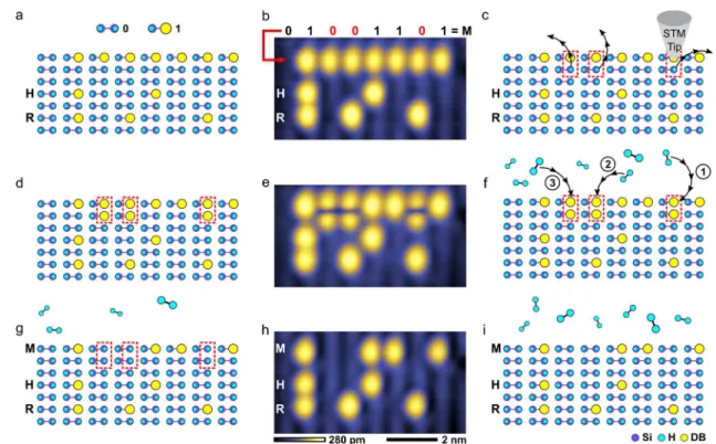
Figure 3. M-HR (I = 50 pA, T = 4.5 K, 8 × 8 nm2). (a) (V = 1.4 V) STM image of an 8-bit DB memory array, with a fabrication error, taken to visualize the location of the surface hydrogen atoms. When imaging DB structures in empty states, there is a dynamic interplay between charge injection from the tip, discharging rates into the bulk, and tip-induced band bending, which causes a dark region to appear surrounding the structure.31,55,56It has also been proposed that the additional corrugation between neighboring DBs in the structure is due to contributions from excited states.10 (b) (V = −1.6 V) The same structure in (a), taken at a negative sample bias to better visualize the location of the DBs in the array. (c) (V = 1.4 V) STM image taken after the erroneous DB in (a) was converted into an interdimer site, by removing an additional hydrogen atom from the surface. (d) (V = −1.6 V) STM image taken immediately after (c) (52 s later), during which time the interdimer site reacted with an ambient hydrogen molecule to erase the erroneous DB. (e) (V = −1.6 V) Error-free 8-bit memory array structure, after the removal of the correct hydrogen atom from the surface. (f) (V = −1.6 V) Same structure shown in (e) unchanged after 6 days in an environment of an estimated pressure of 1 × 10⁻⁹Torr of hydrogen gas.
the neighboring bit. However, the arrays can be redesigned to incorporate M-HR as the main means of altering the stored information by shifting the geometry by 90° and redefining the area of a unit memory cell (Supplementary Figure 8b,c). In these alternative designs, each bit/DB can now be converted into an interdimer site to be rewritten as needed, unlike in the original implementation6 (Supplementary Figure 8a). By incorporating M-HR, the maximum storage density of the arrays is reduced from 1.70 bits per nm2to 1.36 bits per nm2
(Supplementary Figure 8b). The slight reduction in maximum storage density is compensated for by the simplicity and increased maximum speed of rewriting multiple bits, compared to HR (where the tip needs to travel away from the array to be loaded with multiple hydrogen atoms). Additionally, the unlimited local supply of hydrogen molecules removes any restriction on the number of possible write/rewrite cycles of the memory arrays.
We have demonstrated the use of M-HR to rewrite a small 24-bit memory array created using automated HL6 (Figure 4a,b). With M-HR, once the bits/DBs to be overwritten were converted into interdimer sites (see Methods), the tip was available to perform other tasks, while the repassivation could proceed in the background in a quasi-parallel fashion. We were able to use the tip to record images in between the acquisition ofFigure 4e,h (Supplementary Figure 9), as well as condition it further. This is unlike the HR procedure, which is inherently
serial, where the tip is actively involved during the entire repassivation process.
Since the process to replace surface atoms now only requires the technique for atom removal, techniques like M-HR provide a possible path forward from purely scanned probe-based atomic-scale fabrication. In the future, as ion and electron beam-based fabrication techniques become increasingly capable of imaging and manipulating single atoms,59,60 it is conceivable that the STM probe used to remove hydrogen atoms from the silicon surface could eventually be replaced. Should such a transition occur for the removal of atoms, M-HR presents the ability to add material back in a controlled manner, with the prospect of completely scanned probe-free writing/rewriting for data storage applications.
CONCLUSIONS
We have demonstrated a process that can be used to conveniently characterize the charge occupation, or changes, of fabricated DB structures down to a single electron level, with only an STM. Using HL and HR techniques to create and erase single isolated DBs with a charge of one electron, the shifts of a feature in the I(V) spectrum of a sensor DB can be calibrated to compare against those induced by a structure of interest. With this technique, we verified prior AFM results with an STM.
Figure 4. Rewriting a 24-bit memory array (V = −1.65 V, I = 50 pA, T = 4.5 K, 4 × 7.5 nm2). (a) Schematic of a 24-bit memory array created from DBs. The first line of the array is blank (01111111), the next two lines are the ASCII binary forms of the letters H (01001000) and R (01010010). (b) STM image of the 24-bit array created from DBs (using automated hydrogen lithography)6with a storage density of 1.36
bits per nm2. The data in the first line will be rewritten to store the letter M (01001101). (c) Using the automated STM tip, the surface hydrogen atoms highlighted in red will be removed to create reactive interdimer sites in order to rewrite the array. (d) A schematic of the surface after the three hydrogen atoms shown in (c) have been removed. (e) An STM image of the 24-bit DB array after three surface hydrogen atoms have been removed with the STM tip to create interdimer sites. (f) Hydrogen gas is introduced into the vacuum chamber to bind with the interdimer sites (highlighted in red). The three reactions proceeded in the order indicated. The full sequence of images is available inSupplementary Figure 9. (g) The first line of the array shown in (a) has been rewritten to the letter M, now that hydrogen molecules have dissociatively reacted with the interdimer sites shown in (d). (h) STM image of the 24-bit memory array after the interdimer sites have reacted with hydrogen molecules, rewriting the stored information. (i) The remaining hydrogen gas in the chamber does not react with the isolated DBs in the array and can be used in further rewriting operations.
ACS Nano Article
DOI:10.1021/acsnano.9b07637
ACS Nano2020, 14, 2947−2955 2952
We electronically detected the binding event of a hydrogen molecule at a prepared interdimer site on the surface, with the tip laterally removed by >10 nm. We expect that the same techniques employed here can also be applied to study the adsorption dynamics of additional molecules of technological interest, including diverse alkenes and aromatic molecules by using other tailored DB reactive sites (such as in Supple-mentary Figure 1). The interdimer and intradimer sites presented here can directly be used to study cycloaddition reactions on silicon,17 including with ethylene.15,61 Due to their charged nature, reactive DB sites can also be directly integrated into field-controlled atomic electronic circuitry designs,5providing yet another route for sensing applications. The ability to exactly position reactive sites in a particular area will also further the study of the effects of atomic-scale surface variations on the reactivity of otherwise identical DB sites.
We applied the ability to create selective DB sites tailored to react with hydrogen molecules as a more efficient means to correct fabrication errors in automated HL. The unified technique of atom removal and replacement offers several improvements over HR, including no longer requiring external hydrogen atoms to be brought in on a probe. M-HR was then incorporated into alternative designs of atomic memory arrays to improve the future rewriting speeds and overall usability of atom-based data storage, illustrated with a small-scale demonstration. Although this demonstration only contained 24 bits, there are no physical limitations preventing the technique from scaling to larger arrays.
METHODS
Equipment.All measurements were performed with a commercial low-temperature Omicron LT-STM (or LT-AFM) operating at 4.5 K. Polycrystalline tungsten wire (0.25 mm diameter) was used for the STM tips. The tips were electrochemically etched in a solution of 2 M NaOH, then were processed under ultrahigh vacuum (UHV) conditions in a field ion microscope to further sharpen them via a nitrogen gas etching process.62
Sample Preparation.The highly arsenic-doped Si(100) (0.003− 0.004 Ω·cm) samples were degassed at 600 °C under UHV conditions for 24 h. Using resistive heating, the samples were brought to a temperature of 1250 °C three to five times via rapid flashes in order to remove all native oxide. We then exposed the samples to 1 × 10⁻⁶ Torr of 99.999% pure hydrogen gas (or 99.7% pure deuterium gas), flowed through a liquid nitrogen trap. A nearby tungsten filament held at 1900 °C was used to crack the gas into its atomic constituents. The samples were exposed to the gas for 120 s without heating, then were rapidly flashed to 1250 °C. The temperature was then quickly brought down to 330 °C for 150 s, giving the hydrogen(or deuterium)-terminated 2 × 1 surface reconstruction.
Reducing Tip Field Effects. For sharp tips/probes, with radii of <20 nm, there is a significant reduction in the strength of the local tip field and charge injection/extraction along the surface with increasing lateral separation from the tip.10,31,55,56,63−65Experimentally, on this
substrate, the effects of charge injection from an STM tip into a DB have been observed with lateral separations of approximately 2−4 nm depending on the tip radius,10,31,55with sharper tips requiring closer tip-DB separations for charge injection to occur.31,55The effects of the tip field, without the injection of charge, have been observed at up to 7 nm of lateral tip-DB separation, depending on the tip geometry and applied voltage.10,31,37,55By working with single atom tips and
restricting voltages to between −1.2 V and −1.6 V, and additionally characterizing structures five or more nanometers laterally removed from the STM tip, we greatly reduce the possible effects of both charge injection and field perturbations.
Electronic Molecular Detection. Once a sensor DB was identified, a baseline I(V) spectrum was recorded, and the desired
number of interdimer sites were created. The STM tip was then positioned over the sensor DB, and the measurement program was initiated to periodically record the I(V) spectrum. We then introduced 99.999% pure hydrogen gas into the system until a pressure of 4 × 10⁻⁷Torr was achieved external to the cryo-shielding,
via a manual leak valve (the initial base pressure inside of the STM
external to the cryo-shielding was 5 × 10⁻¹¹Torr). The time interval was selected such that the entire I(V) spectrum of the sensor DB could be recorded (both forward and backward sweeps), and the hydrogen gas pressure could be manually corrected in between measurements. The time window also provided sufficient delay for the majority of the mechanical vibrations of the STM tip (due to the manual actuation of the leak valve) to dissipate before each spectrum was acquired. To undertake real-time measurements, where the acquisition of the full I(V) spectrum is not required, the tip can be held at a fixed voltage and the tunneling current (or z-height) can be monitored for sudden changes in the DB conductivity (
Supple-mentary Figure 10). The jump in the tunneling current can be
detected in an identical way to the detection of current changes used in HL, with a maximum sampling rate of 10 kHz.6
Estimating Pressure.Using the observations of the reaction time of interdimer sites with hydrogen molecules, we can estimate a bound on the pressure of hydrogen inside the shielding, where there is no pressure sensor available. To estimate the hydrogen pressure in the vicinity of the tip and sample (Pest), we assume a perfect sticking coefficient due to the barrierless nature of the reaction of molecular hydrogen with interdimer sites38−40,42(along with our observation of
the reaction at 4.5 K). Using the ideal gas law, and the thermal distribution of the velocities and number of hydrogen molecules incident on the silicon surface, the pressure is given by66
P d m k T t (2 ) est H b 1/2 rx 2 π = × × × × (1) where d is the number of surface sites per unit area (for Si(100)-2 × 1: d ≈ 1019sites per m2), mH
2is the mass of a molecule of hydrogen,
kbis the Boltzmann constant, T is the temperature (4.5 K), and trxis the observed time for all sites to react. Using conventional sequential STM image acquisition for slower dynamics, we observed three interdimer sites react over 45 h (Supplementary Figure 6), giving an estimated pressure of approximately 1 × 10⁻¹² Torr. With observations taken using the electronic detection technique after the introduction of H2 into the chamber, including Figure 2, we estimated a local pressure of approximately 1 × 10⁻¹⁰ Torr. In
Supplementary Figure 7, all three interdimer sites reacted within 120 s
after creating the third interdimer site. Including this observation, along withFigure 3(52 s), we estimated a pressure at that time of at least 1 × 10⁻⁹Torr near the sample surface, recognizing that the reactions may have occurred in <120 s inSupplementary Figure 7. Given an H2pressure of 1 × 10⁻⁹Torr at a temperature of 4.5 K,eq 1 predicts that trx≈ 60 s. The average measured trxof the interdimer sites at an estimated H2pressure of approximately 1 × 10⁻⁹Torr at 4.5 K agrees well with this prediction. The agreement between the predicted and the measured reaction time further supports our notion that the hydrogen molecules arrive at the interdimer sites from the gas phase.
Rewriting Atomic Memory Array.Once the bits/DBs identified to be rewritten were converted into interdimer sites (Figure 4), hydrogen gas was introduced into the vacuum chamber to achieve the same conditions as in Figure 3. Because the initial hydrogen background pressure in the chamber external to the cryo-shielding was low (<1 × 10⁻¹¹ Torr), it took approximately 30 min before the pressure in proximity to the tip and sample was sufficiently high for the first M-HR event to occur. The remaining events occurred within 1 min of each other after an approximate pressure of 1 × 10⁻⁹Torr was achieved near the sample surface.
ASSOCIATED CONTENT
*
S Supporting InformationThe Supporting Information is available free of charge on the
ACS Publications websiteat DOI:10.1021/acsnano.9b07637. Supplementary Figures 1−10 (PDF) AUTHOR INFORMATION Corresponding Author *E-mail:[email protected]. ORCID Roshan Achal:0000-0003-4879-3508 Jeremiah Croshaw:0000-0001-9164-1556 Taleana R. Huff:0000-0002-6876-8265 Author Contributions
R.A. conceived of the memory designs, molecular hydrogen repassivation procedure, molecule detection procedure, and performed all STM experiments. M.R., R.A., and R.A.W. conceived of the charge characterization experiment. J.C. and R.A. developed the molecule detection program. T.H. performed the supplementary AFM measurements. R.A.W. supervised the project. R.A. prepared the manuscript. All authors participated in the review and discussion of the manuscript and results.
Notes
The authors declare the following competing financial interest(s): A patent application is in process related to molecular hydrogen repassivation and memory designs as described in the manuscript. All of the authors are affiliated with Quantum Silicon, Inc. (QSi). QSi is seeking to commercialize atomic silicon quantum dot-based technologies.
ACKNOWLEDGMENTS
The authors thank M. Salomons and M. Cloutier for their technical assistance, J. Pitters for helpful discussions, and J. Phillips for proofreading the manuscript. We would like to also thank NSERC, AITF, NRC, and QSi for their financial support.
REFERENCES
(1) Schofield, S. R.; Curson, N. J.; Simmons, M. Y.; Rueß, F. J.; Hallam, T.; Oberbeck, L.; Clark, R. G. Atomically Precise Placement of Single Dopants in Si. Phys. Rev. Lett. 2003, 91, 136104.
(2) Fuechsle, M.; Miwa, J. A.; Mahapatra, S.; Ryu, H.; Lee, S.; Warschkow, O.; Hollenberg, L. C. L.; Klimeck, G.; Simmons, M. Y. A Single-Atom Transistor. Nat. Nanotechnol. 2012, 7, 242−246.
(3) Broome, M. A.; Gorman, S. K.; House, M. G.; Hile, S. J.; Keizer, J. G.; Keith, D.; Hill, C. D.; Watson, T. F.; Baker, W. J.; Hollenberg, L. C. L.; Simmons, M. Y. Two-Electron Spin Correlations in Precision Placed Donors in Silicon. Nat. Commun. 2018, 9, 980.
(4) Ramanayaka, A. N.; Kim, H.-S.; Tang, K.; Wang, X.; Silver, R. M.; Stewart, M. D.; Pomeroy, J. M. STM Patterned Nanowire Measurements Using Photolithographically Defined Implants in Si(100). Sci. Rep. 2018, 8, 1790.
(5) Huff, T.; Labidi, H.; Rashidi, M.; Livadaru, L.; Dienel, T.; Achal, R.; Vine, W.; Pitters, J.; Wolkow, R. A. Binary Atomic Silicon Logic.
Nat. Electron. 2018, 1, 636−643.
(6) Achal, R.; Rashidi, M.; Croshaw, J.; Churchill, D.; Taucer, M.; Huff, T.; Cloutier, M.; Pitters, J.; Wolkow, R. A. Lithography for Robust and Editable Atomic-Scale Silicon Devices and Memories.
Nat. Commun. 2018, 9, 2778.
(7) Crane, E.; Kölker, A.; Stock, T. Z.; Stavrias, N.; Saeedi, K.; van Loon, M. A. W.; Murdin, B. N.; Curson, N. J. Hydrogen Resist Lithography and Electron Beam Lithography for Fabricating Silicon
Targets for Studying Donor Orbital States. J. Phys.: Conf. Ser. 2018,
1079, 012010.
(8) Ballard, J. B.; Owen, J. H. G.; Owen, W.; Alexander, J. R.; Fuchs, E.; Randall, J. N.; Von Ehr, J. R.; McDonnell, S.; Dick, D. D.; Wallace, R. M.; Chabal, Y. J.; Bischof, M. R.; Jaeger, D. L.; Reidy, R. F.; Fu, J.; Namboodiri, P.; Li, K.; Silver, R. M. Pattern Transfer of Hydrogen Depassivation Lithography Patterns into Silicon with Atomically Traceable Placement and Size Control. J. Vac. Sci. Technol., B:
Nanotechnol. Microelectron.: Mater., Process., Meas., Phenom. 2014, 32,
041804.
(9) Møller, M.; Jarvis, S. P.; Guérinet, L.; Sharp, P.; Woolley, R.; Rahe, P.; Moriarty, P. Automated Extraction of Single H Atoms with STM: Tip State Dependency. Nanotechnology 2017, 28, 075302.
(10) Schofield, S. R.; Studer, P.; Hirjibehedin, C. F.; Curson, N. J.; Aeppli, G.; Bowler, D. R. Quantum Engineering at the Silicon Surface Using Dangling Bonds. Nat. Commun. 2013, 4, 1649.
(11) Hersam, M. C.; Guisinger, N. P.; Lyding, J. W. Isolating, Imaging, and Electrically Characterizing Individual Organic Molecules on the Si(100) Surface with the Scanning Tunneling Microscope. J.
Vac. Sci. Technol., A 2000, 18, 1349−1353.
(12) Mayne, A. J.; Soukiassian, L.; Commaux, N.; Comtet, G.; Dujardin, G. Molecular Molds. Appl. Phys. Lett. 2004, 85, 5379−5381. (13) Dürr, M.; Hu, Z.; Biedermann, A.; Höfer, U.; Heinz, T. F. Real-Space Study of the Pathway for Dissociative Adsorption of H2 on Si(001). Phys. Rev. Lett. 2002, 88, 046104.
(14) Dürr, M.; Höfer, U. Dissociative Adsorption of Molecular Hydrogen on Silicon Surfaces. Surf. Sci. Rep. 2006, 61, 465−526.
(15) Mette, G.; Schwalb, C. H.; Dürr, M.; Höfer, U. Site-Selective Reactivity of Ethylene on Clean and Hydrogen Precovered Si(0 0 1).
Chem. Phys. Lett. 2009, 483, 209−213.
(16) Xin, N.; Guan, J.; Zhou, C.; Chen, X.; Gu, C.; Li, Y.; Ratner, M. A.; Nitzan, A.; Stoddart, J. F.; Guo, X. Concepts in the Design and Engineering of Single-Molecule Electronic Devices. Nat. Rev. Phys. 2019, 1, 211−230.
(17) Bent, S. F. Organic Functionalization of Group IV Semi-conductor Surfaces: Principles, Examples, Applications, and Prospects.
Surf. Sci. 2002, 500, 879−903.
(18) Hersam, M. C.; Guisinger, N. P.; Lyding, J. W. Silicon-Based Molecular Nanotechnology. Nanotechnology 2000, 11, 70−76.
(19) Piva, P. G.; DiLabio, G. A.; Pitters, J. L.; Zikovsky, J.; Rezeq, M.; Dogel, S.; Hofer, W. A.; Wolkow, R. A. Field Regulation of Single-Molecule Conductivity by a Charged Surface Atom. Nature 2005,
435, 658−661.
(20) Wolkow, R. A. Controlled Molecular Adsorption on Silicon: Laying a Foundation for Molecular Devices. Annu. Rev. Phys. Chem. 1999, 50, 413−441.
(21) Metzger, R. M. Unimolecular Electronics. Chem. Rev. 2015,
115, 5056−5115.
(22) Lörtscher, E. Wiring Molecules into Circuits. Nat. Nanotechnol. 2013, 8, 381−384.
(23) Aragonès, A. C.; Darwish, N.; Ciampi, S.; Sanz, F.; Gooding, J. J.; Díez-Pérez, I. Single-Molecule Electrical Contacts on Silicon Electrodes under Ambient Conditions. Nat. Commun. 2017, 8, 15056. (24) Song, H.; Reed, M. A.; Lee, T. Single Molecule Electronic Devices. Adv. Mater. 2011, 23, 1583−1608.
(25) Warschkow, O.; Curson, N. J.; Schofield, S. R.; Marks, N. A.; Wilson, H. F.; Radny, M. W.; Smith, P. V.; Reusch, T. C. G.; McKenzie, D. R.; Simmons, M. Y. Reaction Paths of Phosphine Dissociation on Silicon (001). J. Chem. Phys. 2016, 144, 014705.
(26) Wilson, H. F.; Warschkow, O.; Marks, N. A.; Curson, N. J.; Schofield, S. R.; Reusch, T. C. G.; Radny, M. W.; Smith, P. V.; McKenzie, D. R.; Simmons, M. Y. Thermal Dissociation and Desorption of PH3 on Si(001): A Reinterpretation of Spectroscopic Data. Phys. Rev. B: Condens. Matter Mater. Phys. 2006, 74, 195310.
(27) Wakayama, Y.; Hill, J. P.; Ariga, K. Real-Time STM Observation of Molecular Dynamics on a Metal Surface. Surf. Sci. 2007, 601, 3984−3987.
(28) Schaffert, J.; Cottin, M. C.; Sonntag, A.; Karacuban, H.; Bobisch, C. a.; Lorente, N.; Gauyacq, J.-P.; Möller, R. Imaging the
ACS Nano Article
DOI:10.1021/acsnano.9b07637
ACS Nano2020, 14, 2947−2955 2954
Dynamics of Individually Adsorbed Molecules. Nat. Mater. 2013, 12, 223−227.
(29) Engelund, M.; Godlewski, S.; Kolmer, M.; Zuzak, R.; Such, B.; Frederiksen, T.; Szymonski, M.; Sánchez-Portal, D. The Butterfly − a Well-Defined Constant-Current Topography Pattern on Si(001):H and Ge(001):H Resulting from Current-Induced Defect Fluctuations.
Phys. Chem. Chem. Phys. 2016, 18, 19309−19317.
(30) Godlewski, S.; Kawai, H.; Kolmer, M.; Zuzak, R.; Echavarren, A. M.; Joachim, C.; Szymonski, M.; Saeys, M. Single-Molecule Rotational Switch on a Dangling Bond Dimer Bearing. ACS Nano 2016, 10, 8499−8507.
(31) Taucer, M.; Livadaru, L.; Piva, P. G.; Achal, R.; Labidi, H.; Pitters, J. L.; Wolkow, R. A. Single-Electron Dynamics of an Atomic Silicon Quantum Dot on the H−Si(100)−(2 × 1) Surface. Phys. Rev.
Lett. 2014, 112, 256801.
(32) Pitters, J. L.; Wolkow, R. A. Detailed Studies of Molecular Conductance Using Atomic Resolution Scanning Tunneling Micros-copy. Nano Lett. 2006, 6, 390−397.
(33) Chao, K.-J.; Smith, A. R.; Shih, C.-K. Direct Determination of Exact Charge States of Surface Point Defects Using Scanning Tunneling Microscopy: As Vacancies on GaAs (110). Phys. Rev. B:
Condens. Matter Mater. Phys. 1996, 53, 6935−6938.
(34) Gohlke, D.; Mishra, R.; Restrepo, O. D.; Lee, D.; Windl, W.; Gupta, J. Atomic-Scale Engineering of the Electrostatic Landscape of Semiconductor Surfaces. Nano Lett. 2013, 13, 2418−2422.
(35) Huff, T.; Labidi, H.; Rashidi, M.; Koleini, M.; Achal, R.; Salomons, M. H.; Wolkow, R. A. Atomic White-Out: Enabling Atomic Circuitry Through Mechanically Induced Bonding of Single Hydro-gen Atoms to a Silicon Surface. ACS Nano 2017, 11, 8636−8642.
(36) Pavliček, N.; Majzik, Z.; Meyer, G.; Gross, L. Tip-Induced Passivation of Dangling Bonds on Hydrogenated Si(100)-2 × 1. Appl.
Phys. Lett. 2017, 111, 053104.
(37) Huff, T. R.; Dienel, T.; Rashidi, M.; Achal, R.; Livadaru, L.; Croshaw, J.; Wolkow, R. A. Electrostatic Landscape of a Hydrogen-Terminated Silicon Surface Probed by a Moveable Quantum Dot.
ACS Nano 2019, 13, 10566−10575.
(38) Pehlke, E. Highly Reactive Dissociative Adsorption of Hydrogen Molecules on Partially H-Covered Si(001) Surfaces: A Density-Functional Study. Phys. Rev. B: Condens. Matter Mater. Phys. 2000, 62, 12932−12939.
(39) Narita, Y.; Inanaga, S.; Namiki, A. Kinetics of Hydrogen Adsorption and Desorption on Si(100) Surfaces. J. Appl. Phys. 2013,
113, 234309.
(40) Filippi, C.; Healy, S. B.; Kratzer, P.; Pehlke, E.; Scheffler, M. Quantum Monte Carlo Calculations of H2 Dissociation on Si(001).
Phys. Rev. Lett. 2002, 89, 166102.
(41) Warschkow, O.; Wilson, H. F.; Marks, N. A.; Schofield, S. R.; Curson, N. J.; Smith, P. V.; Radny, M. W.; McKenzie, D. R.; Simmons, M. Y. Phosphine Adsorption and Dissociation on the Si(001) Surface: An Ab Initio Survey of Structures. Phys. Rev. B:
Condens. Matter Mater. Phys. 2005, 72, 125328.
(42) Kanai, Y.; Tilocca, A.; Selloni, A.; Car, R. First-Principles String Molecular Dynamics: An Efficient Approach for Finding Chemical Reaction Pathways. J. Chem. Phys. 2004, 121, 3359−3367.
(43) Rashidi, M.; Burgess, J. A. J.; Taucer, M.; Achal, R.; Pitters, J. L.; Loth, S.; Wolkow, R. A. Time-Resolved Single Dopant Charge Dynamics in Silicon. Nat. Commun. 2016, 7, 13258.
(44) Rashidi, M.; Lloyd, E.; Huff, T. R.; Achal, R.; Taucer, M.; Croshaw, J. J.; Wolkow, R. A. Resolving and Tuning Carrier Capture Rates at a Single Silicon Atom Gap State. ACS Nano 2017, 11, 11732−11738.
(45) Pitters, J. L.; Piva, P. G.; Wolkow, R. A. Dopant Depletion in the near Surface Region of Thermally Prepared Silicon (100) in UHV.
J. Vac. Sci. Technol., B: Nanotechnol. Microelectron.: Mater., Process., Meas., Phenom. 2012, 30, 021806.
(46) Haider, M. B.; Pitters, J. L.; Dilabio, G. a.; Livadaru, L.; Mutus, J. Y.; Wolkow, R. A. Controlled Coupling and Occupation of Silicon Atomic Quantum Dots at Room Temperature. Phys. Rev. Lett. 2009,
102, 046805.
(47) Pires, R. G.; Dickstein, R. M.; Titcomb, S. L.; Anderson, R. L. Carrier Freezeout in Silicon. Cryogenics 1990, 30, 1064−1068.
(48) Dürr, M.; Raschke, M. B.; Pehlke, E.; Höfer, U. Structure Sensitive Reaction Channels of Molecular Hydrogen on Silicon Surfaces. Phys. Rev. Lett. 2001, 86, 123−126.
(49) Buehler, E. J.; Boland, J. J. Dimer Preparation That Mimics the Transition State for the Adsorption of H2 on the Si(100)-2 × 1 Surface. Science 2000, 290, 506−509.
(50) Züttel, A. Materials for Hydrogen Storage. Mater. Today 2003,
6, 24−33.
(51) Leung, W. B.; March, N. H.; Motz, H. Primitive Phase Diagram for Hydrogen. Phys. Lett. A 1976, 56, 425−426.
(52) Jarvis, S.; Sweetman, A.; Bamidele, J.; Kantorovich, L.; Moriarty, P. Role of Orbital Overlap in Atomic Manipulation. Phys.
Rev. B: Condens. Matter Mater. Phys. 2012, 85, 235305.
(53) Rashidi, M.; Croshaw, J.; Mastel, K.; Tamura, M.; Hosseinzadeh, H.; Wolkow, R. A. Autonomous Atomic Scale Manufacturing Through Machine Learning. 2019, arXiv.org e-Print
archive 1902.08818.https://arxiv.org/abs/1902.08818(accessed June 13, 2019).
(54) Rashidi, M.; Wolkow, R. A. Autonomous Scanning Probe Microscopy In Situ Tip Conditioning through Machine Learning. ACS
Nano 2018, 12, 5185−5189.
(55) Achal, R. Detailed Study of Atomic Silicon Dangling Bond Charge State Dynamics on the Surface of Hydrogen Terminated Silicon (100)-2 × 1. MS Thesis; University of Alberta, Alberta, Canada, 2015.
(56) Livadaru, L.; Pitters, J.; Taucer, M.; Wolkow, R. A. Theory of Nonequilibrium Single-Electron Dynamics in STM Imaging of Dangling Bonds on a Hydrogenated Silicon Surface. Phys. Rev. B:
Condens. Matter Mater. Phys. 2011, 84, 205416.
(57) McEllistrem, M.; Allgeier, M.; Boland, J. J. Dangling Bond Dynamics on the Silicon (100)-2 × 1 Surface: Dissociation, Diffusion, and Recombination. Science 1998, 279, 545−548.
(58) Schwalb, C. H.; Dürr, M.; Höfer, U. High-Temperature Investigation of Intradimer Diffusion of Hydrogen on Si(001). Phys.
Rev. B: Condens. Matter Mater. Phys. 2010, 82, 193412.
(59) Susi, T.; Kotakoski, J.; Kepaptsoglou, D.; Mangler, C.; Lovejoy, T. C.; Krivanek, O. L.; Zan, R.; Bangert, U.; Ayala, P.; Meyer, J. C.; Ramasse, Q. Silicon-Carbon Bond Inversions Driven by 60-Kev Electrons in Graphene. Phys. Rev. Lett. 2014, 113, 115501.
(60) Dyck, O.; Kim, S.; Jimenez-Izal, E.; Alexandrova, A. N.; Kalinin, S. V.; Jesse, S. Building Structures Atom by Atom via Electron Beam Manipulation. Small 2018, 14, 1801771.
(61) Pecher, J.; Mette, G.; Dürr, M.; Tonner, R. Site-Specific Reactivity of Ethylene at Distorted Dangling-Bond Configurations on Si(001). ChemPhysChem 2017, 18, 357−365.
(62) Rezeq, M.; Pitters, J.; Wolkow, R. Tungsten Nanotip Fabrication by Spatially Controlled Field-Assisted Reaction with Nitrogen. J. Chem. Phys. 2006, 124, 204716.
(63) Feenstra, R. M. Electrostatic Potential for a Hyperbolic Probe Tip near a Semiconductor. J. Vac. Sci. Technol., B: Microelectron.
Process. Phenom. 2003, 21, 2080.
(64) Feenstra, R. M. A Prospective: Quantitative Scanning Tunneling Spectroscopy of Semiconductor Surfaces. Surf. Sci. 2009,
603, 2841−2844.
(65) Lee, D.; Gohlke, D.; Benjamin, A.; Gupta, J. A. Influence of the Local Environment on Mn Acceptors in GaAs. J. Phys.: Condens.
Matter 2015, 27, 154202.
(66) Freire, V.-M.; Ramirez, A.; Pascual, E.; Bertran, E.; Andujar, J.-L. Investigation of Monolayer-Formation Time for the Synthesis of Graphene on Copper/Nickel/Silicon Using Very-Low Pressure Pulses of Methane. 2014, arXiv.org e-Print archive 1406.2640.https://arxiv.