Analysis and Simulation of a CIC-Filter-Based
Multiplexed-Input Sigma-Delta Analog-to-Digital Converter
by
Seungmyon Park
SUBMITTED TO THE DEPARTMENT OF
ELECTRICAL ENGINEERING AND COMPUTER SCIENCE IN PARTIAL FULFILLMENT OF THE REQUIREMENTS FOR
THE DEGREE OF MASTER OF ENGINEERING
IN ELECTRICAL ENGINEERING AND COMPUTER SCIENC MASSACHUSETTS INSTITUTE AT THE MASSACHUSETTS INSTITUTE OF TECHNOLOG OF TECHNOLOGY
May 1,2001 e U > JUL 11 200 © 2001 Seungmyon Park. All rights reserved. LIBRARIES The author hereby grants to MIT permission to reproduce and to distribute publicly paper and
electronic copies of this thesis document in whole or in part.
Signature of Author
Department of Electrical Engp einin'd Computer Science Certified by
Paul Ward Charles Stark Draper Laboratory Thesis Supervisor Certified by __ _ _ _ _ _ _ _ _ _ _ _ _ _ _ _ _ _ _ _ _ _ __ _ _ _ _ _
Professor James K§ Roberge Professor of Electricaltngneering and-9mputer Science Thasis Advisor Accepted by
Frolessor Arthur C. Smith Chairman, Departmental Committee on Graduate Theses
Analysis and Simulation of a CIC-Filter-Based
Multiplexed-Input Sigma-Delta Analog-to-Digital Converter
by
Seungmyon Park
SUBMITTED TO THE DEPARTMENT OF
ELECTRICAL ENGINEERING AND COMPUTER SCIENCE ON MAY 23, 2001
IN PARTIAL FULFILLMENT OF THE REQUIREMENTS FOR THE DEGREE OF MASTER OF ENGINEERING
IN ELECTRICAL ENGINEERING AND COMPUTER SCIENCE AT THE MASSACHUSETTS INSTITUTE OF TECHNOLOGY
Abstract
Draper Laboratory's MEMS inertial instruments used for navigation demand extremely high dynamic range and low power consumption. In this thesis, a multiplexed-input sigma-delta analog-to-digital converter using a cascaded integrator-comb filter used in the MEMS instrument electronics is analyzed and simulated in order to determine the tradeoff between resolution and multiplexing rate. A simulation model created in Simulink is used in order to verify the correctness of the analysis and to predict performance. A VHDL simulation model is also created in order to further evaluate performance and to check synthesizability and power consumption. Simulation data shows that the design evaluated is capable of providing a signal-to-noise ratio of up to
~100dB when four slowly-varying ( 5 5Hz) inputs are multiplexed.
Technical Supervisor: Paul Ward
Title: Group Leader, Charles Stark Draper Laboratory Thesis Advisor: Professor James K. Roberge
ACKNOWLEDGMENT
May 23, 2001
This thesis was prepared at The Charles Stark Draper Laboratory, Inc., under Internal Company Sponsored Research Project 3050, HPG1 ASIC Test and Evaluation. Publication of this thesis does not constitute approval by Draper or the sponsoring agency of the findings or conclusions contained herein. It is published for the exchange and stimulation of ideas.
Acknowledgements
I would first like to thank the Charles Stark Draper Laboratory for sponsoring my work on this project. I would also like to thank my Draper supervisor Paul Ward and faculty advisor Professor James Roberge for their invaluable technical guidance, insight, and patience. In addition, I would like to thank David McGorty of Draper Laboratory, for this project could not have been completed without his technical guidance. I would also like to express my gratitude towards the following people at Draper who made this thesis possible: Bob Kelley, Phil Juang, Amy Duwel, and Rob Bousquet. Finally, I would like to thank Dr. Marc Weinberg for providing me the opportunity to work at Draper.
Contents
1 Introduction
1.1 Background . . . . 1.1.1 Application . . . . 1.1.2 Choosing the ADC Architecture . . 1.2 Purpose and Organization of this Paper. . 1.3 Definition of Resolution . . . . 2 Analysis of the Draper]
2.1 Sigma-Delta Modulato 2.1.1 Sources of Nois 2.1.2 Signal and Nois 2.1.3 Performance .. Design r - - - - - -e . . . . se Transfer Fuinctions. 2.2 Digital Filter . . . . 2.2.1 Overview . . . . 2.2.2 Architecture . . . . 2.3 Combined Analysis . . . . 2.3.1 Signal and Noise Power . . . 2.3.2 Downsampling . . . . 2.3.3 Obtaining Filter Parameters 2.4 Results . . . . 2.4.1 Filter Parameters . . . . 2.4.2 Multiplexing . . . . 12 12 12 13 17 17 19 . . . 19 21 23 25 . . . 27 27 28 . . . 30 30 32 33 . . . 34 34 34 . . . . . . . .
3 Simulation Using Simulink 3.1 Overview . . . . 3.2 Sigma-Delta Modulator . . . . 3.2.1 Thermal Noise . . . . 3.3 CIC Filter . . . . 3.4 Results . . . . 3.4.1 SDM Settling Time . 3.4.2 ADC Performance . . . . 4 Simulation of the Hardware Using
4.1 Overview of the Test Bench . . . 4.2 Thermal Noise Blocks . . . . 4.3 VHDL Implementation of the SDIM 4.4 VHDL Implementation of the CIC
4.4.1 Architecture . . . . 4.4.2 Register Sizing . . . . 4.4.3 Performance . . . . 4.5 Design Guidelines . . . . 4.5.1 Truncation Noise Analysis 4.5.2 Approach to Design . . . . 4.5.3 Multiplexing . . . . 4.6 Synthesis of VHDL Code . . . . . 4.6.1 Synthesizability and Power 4.6.2 Alternate Architecture . . VHD Filter Consi 5 Conclusion Bibliography A Matlab Scripts A.1 rn-choose.m... .. ... A.2 cic-filt.spec.m ... .. .. . ... .. . ... . . . .. ... . . IL . . . . . . . . 40 40 41 43 43 44 44 47 52 52 54 57 61 61 64 67 69 69 71 73 74 74 76 78 80 82 82 85
B VHDL Code 87 B.1 read-prn.vhd . . .. .... .... . . . .. . .. . . 87 B .2 prn.vhd . . . .. . . . 89 B .3 prn2.vhd . . . . 91 BA com p-cic.vhd ... 95 B.5 com p-cic2.vhd . . . . 99 B.6 comp-sdm .vhd . . . . 103 B.7 comp-allAb.vhd . . . .. . . . 107
List of Figures
1-1 Flash ADC Architecture . . . . 1-2 Semi-Flash ADC Architecture . . . . 1-3 Sigma-Delta ADC Architecture . . . .
14 14 15
2-1 SDM Block Diagram ... ... 20
2-2 SDM Discrete-Time Representation . . . . 20
2-3 Distribution of e[n] based on input voltage . . . . 21
2-4 Signal and noise transfer functions of the SD2-ADC . . . . 24
2-5 CIC Filter Block Diagram . . . . 28
2-6 Magnitude response of a CIC filter with N=3, R=1000. . . . . 30
2-7 Laboratory measurement of SDM settling time . . . . 36
2-8 Layout of the Test Chip . . . . 37
2-9 SDM Thermal Noise Plot . . . . 38
3-1 Top-level Simulink Model Block Diagram . . . . 41
3-2 SDM Block Diagram . . . . 42
3-3 Details of "Stage 2" of the SDM . . . . 42
3-4 Simulink CIC Filter Implementation . . . . 44
3-5 Modified SDM Block Diagram . . . . 45
3-6 SDM Settling Response . . . . 45
3-7 Decay of the SDM output oscillation . . . . 46
3-8 SDM Simulation PSD .-. . . . . 48
3-9 ADC Output for 5Hz Sine Input . . . . 49 3-10 PSD for ADC Output with 5Hz Sine plus thermal noise input 50
3-11 PSD of Thermal-Noise-Stimulated ADC Output . . . . 50
3-12 ADC Output with Multiplexed Inputs . . . . 51
4-1 VHDL Test Bench Block Diagram . . . . 53
4-2 Shift-Register-Based Pseudorandom Number Generator . . . . 55
4-3 PSDs of simulated thermal noise using prn.vhd . . . . 56
4-4 PSDs of simulated thermal noise using prn2.vhd . . . . 57
4-5 Block Diagram of COMP..SDM . . . . 58
4-6 VHDL-Generated Sine Wave with a Non-Integer Fundamental Frequency 59 4-7 Effect of Resetting the Variable count . . . . 60
4-8 Comparison of VHDL- and Simulink-generated Sine Waves . . . . 60
4-9 PSD of the VHDL and Simulink SDM Outputs . . . . 61
4-10 PSD of the Simulink CIC Filter Output when Using Different SDM M odels . . . . 62
4-11 Block Diagram of the CIC Filter Implemented in VHDL . . . . 62
4-12 Magnitude Response Comparison . . . . 64
4-13 Thermal Noise - Noise Floor Mismatch in VHDL . . . . 68
4-14 Distribution of Truncation Noise . . . . 70 4-15 Comparison of the Predicted and Actual output SNR for R=900, N=3 73
List of Tables
2.1 Filter parameters for various ENOB values . . . . 34
2.2 Settling time for various ENOB values . . . . 36
3.1 SDM settling time for various output widths . . . . 47
3.2 Simulation Summary for a 5Hz, 4V Peak-to-Peak Sine Input . . . . . 50
4.1 Register widths for R and N values used in the Simulink model . . . . 66
4.2 Approximate VHDL ADC signal-to-noise ratio in dB, N=3 . . . . 68
4.3 SNRn for 5Hz, 4V Peak-to-Peak Sinusoid Input, N=3 . . . . 72
4.4 Power consumption for CIC filter, R=900, N=3 . . . . 75
4.5 Power consumption for CIC filter, N=3, B0st = 18 . . . . 75
Chapter 1
Introduction
1.1
Background
1.1.1
Application
Draper Laboratory's high-precision MEMS-based inertial instruments for navigation (such as gyroscopes and accelerometers) are capable of providing an extremely high dynamic range difficult to achieve with conventional techniques. MEMS-based in-struments have the added advantage that the sensor is extremely small, significantly reducing the size of the overall package.
In order to successfully design such sensors, however, one important issue must be resolved. There are several environmental factors that can affect the behavior of MEMS sensors, and to a much lesser degree, the analog circuitry. Because some applications for these instruments demand extremely high dynamic range, the errors induced by these environmental factors can become very significant. For example, changes in temperature can significantly affect the bias and scale factor of MEMS-based instruments. This dilemma is made more significant by the fact that naviga-tional instruments are typically exposed to various different environmental conditions and need to perform consistently in all conditions.
environ-analog signals, called compensation variables, are then digitized by an environ- analog-to-digital converter (ADC). This analog-to-digital data is processed by an on-board computer using a model of the error introduced by the various environmental stimuli on the
MEMS sensor, and the output of the instrument is compensated accordingly.
For the application examined in this paper, it is necessary for the electronics sur-rounding the MEMS sensor to be low-power and minimum-hardware. For this reason, one ADC is shared by multiple compensation variables present in this application. This sharing is done by multiplexing the compensation variables to the ADC input and switching the multiplexer at a constant rate.
The next section briefly discusses various common analog-to-digital conversion techniques, and the design choices made in the ADC examined in this paper.
1.1.2
Choosing the ADC Architecture
Analog-to-Digital Converter ArchitecturesThe topic of analog-to-digital conversion has been studied extensively, and a wide va-riety of conversion methods exists as a result. Some of the more widely-used methods will be mentioned here.
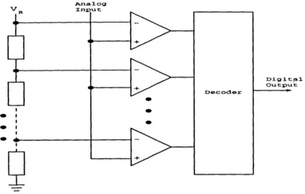
One of the most common type of ADCs is the flash converter. Flash converters can reach very high sampling rates since the only analog building blocks are the comparator and the resistor ladder [1]. Figure 1-1 illustrates the architecture.
As the figure shows, the resistor ladder provides various reference levels for the comparators. Each comparator reads in one reference level and compares it against the analog input, and the collective outputs of the comparators are decoded to form a digital output. The main problem with this architecture is that the number of com-parators increases exponentially with the number of bits. Because of this hardware requirement, the power and area requirements become unreasonably large for a high number of output bits [1]. In addition, because the resistors must be well-matched, extremely precise analog circuitry is needed.
Analo NV tInpl x rl+ Dlecoder Digi tal Ou-tpuIt
Figure 1-1: Flash ADC Architecture
Figure 1-2 shows, the analog-to-digital conversion is done in two stages. In the first stage, a coarse ADC is used to generate N1 most-significant-bits (MSBs) of the output. A digital-to-analog converter (DAC) then converts the output of the coarse ADC and subtracts it from the original analog input to produce a "residue" signal. A second ADC is then used to convert the residue signal and generate N2 least-significant-bits
(LSBs). This ADC architecture is much slower than the flash architecture, but it only requires 2N1 + 2N2 -2 comparators, as opposed to the 2N1+N2 -1 comparators needed
for the flash architecture [1]. However, like the flash converter, semi-flash converters also require high-precision analog circuitry in order to achieve good resolution.
ig Residue
ADC1 DAC
Ni Coars e Bits
ADC2
-N2 Fine Bits
Figure 1-2: Semi-Flash ADC Architecture
There are several other ADC architectures based on the architectures shown so far. The folding and interpolating ADC architecture is similar to the semi-flash
Analo
signal, it uses an analog "folding circuit" that takes in the analog input and produces the same signal. Thus, the coarse and the fine ADCs can convert the input signal almost simultaneously. The multi-stage pipelined ADC is similar to the semi-flash ADC, but it differs in that there are many more stages (Figure 1-2 shows only two), and each stage is pipelined. This variation allows the pipelined ADC to have a much higher sampling rate than the semi-flash ADC [1].
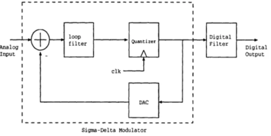
The oversampling sigma-delta ADC architecture is quite different from the ar-chitectures mentioned thus far. Figure 1-3 shows a simplified block diagram of the sigma-delta ADC. ---filter ' Quantizer Analog Digital Input Output clk DAC *- -Sigma-Delta Modulator
Figure 1-3: Sigma-Delta ADC Architecture
As the figure shows, the sigma-delta ADC is divided into two major parts: the delta modulator (SDM) and the digital filter. The basic thought behind sigma-delta modulation is the exchange of resolution in time for resolution in amplitude. As shown in the figure, the quantizer (which can be thought of as a very coarse ADC) quantizes the signal at its input, creating a digital output. This digital output is converted back to an analog signal by the DAC, and the DAC output is compared to the input of the modulator by the subtractor. This negative feedback of the loop suppresses the error caused by the quantizer for the signals falling within the passband of the loop filter [2]. Also, by oversampling the quantizer, noise power is spread over to frequencies beyond the band of interest. Thus, the output of the SDM will have extremely low error in the passband of the ADC (as defined by the loop filter). The digital filter following the SDM has two purposes. First, because the input signal is
oversampled, the output of the SDM must be downsampled to the original analog input bandwidth. However, because there is a large amount of out-of-band noise in the SDM output, simply downsampling the SDM output will result in the aliasing of out-of-band noise into the band of interest. Thus, the digital filter must first remove the out-of-band noise, and then downsample the result. Unlike the architectures based on resistor ladder networks, oversampling sigma-delta converters do not require high-precision analog circuitry. Since its resolution is not limited by imperfections in the circuitry, sigma-delta ADCs are suitable for high-resolution applications that require a complete integration of the circuit onto an application-specific integrated circuit (ASIC) [1]. However, because it oversamples the input, sigma-delta ADCs are more suited for narrow-bandwidth applications. Also, sigma-delta ADCs are much slower than the other architectures mentioned, mostly due to the settling time (the time between the initial reading of the input and the output of the filter becoming valid) of the digital filter.
As mentioned earlier, this section mentions only some of the more commonly-used ADC architectures. Several other architectures not mentioned in this section, such as the successive approximation converters and various types of integrating converters, are still widely used today.
Design Choices
For the application described in the previous section, it was decided that a sigma-delta ADC design would be used. There are several reasons for this choice. One is that sigma-delta ADCs do not require precision analog hardware required by the other architectures, thus reducing cost and complexity of the analog circuitry. The reduction of complexity results in a reduction of area and power. In addition, for low-speed, narrow-band applications, sigma-delta ADCs can achieve a much higher signal-to-noise ratio (SNR) compared to other designs, which makes it suitable for high-precision applications like navigational instruments. One major shortcoming of the sigma-delta design is its large settling time. However, this shortcoming is not a
rate. Because of this low rate of change, even if the multiplexer switchs the input to the sigma-delta ADC at a rate slow enough for the ADC to settle, all of the compensation variables can be digitized at a satisfactory rate.
Prior to the start of this project, the sigma-delta modulator used for the ADC was designed, and the architecture of the filter used for decimation was selected. Some simulation models were created prior to the start of this project to test the feasibility of the planned implementation. The following section discusses the topics covered in this paper.
1.2
Purpose and Organization of this Paper
The main focus of this project is to accurately analyze, model, and simulate the performance of the proposed sigma-delta ADC in order to determine the tradeoff between resolution and the multiplexing of the inputs. This tradeoff can more simply be seen as a tradeoff between resolution and settling time. By understanding this relationship, one can easily design the ADC such that it will achieve the desired resolution for multiple inputs.
The paper is organized as follows. Chapter 2 analyzes the SDM and digital filter mathematically in order to predict its behavior. It also discusses some laboratory work done in order to verify the performance of the SDM. Chapter 3 describes the ADC simulation model created in Simulink and discusses the results obtained in simulation. Chapter 4 discusses the ADC simulation model created in VHDL and the simulation results. It also discusses issues regarding the implementation of the digital filter in hardware, such as synthesizability and power consumption. Chapter 5 is conclusion.
1.3
Definition of Resolution
In order to study the tradeoff between resolution and settling time, the term resolution must be clearly defined. In the analysis shown in the next several chapters, resolution
is defined in terms of effective number of bits (ENOB).
For an ADC with a finite number of bits at the output to represent an analog input signal, some quantization noise at the output is inherent. Given this fact, Engelen [2] determines the maximum possible signal-to-noise ratio (SNR) of an ADC with B output bits, SNRmax, as follows. The maximum amplitude of a sinusoid that does not cause the quantizer to overload is Ama - 2, , where q is the quantization step size. The root-mean-square (rms) amplitude of this sinusoid is then Amax,rms = 2.
The total quantization error power in the Nyquist frequency range is Nq = e. The
12
derivation of this value is explained in Section 2.1.1. The rms amplitude of Nq is
Nq,rms =q. SNRmax is then calculated as
SNRmax = 20 -log10 (A,"r""') = 20 -log10 ( qlV-12)
=B -6.02 + 1.76 (1.1)
For a given B, SNRmax is the highest attainable signal-to-noise ratio. By rear-ranging Equation 1.1, we can solve for B, which can be construed as the effective number of bits for a given SNR.
ENOB = Rmax -1.76 (1.2)
6.02
The concept of ENOB will be used in the following chapters as a guideline for design.
Chapter 2
Analysis of the Draper Design
As mentioned earlier, the sigma-delta ADC design being evaluated is comprised mainly of a second-order sigma-delta modulator (SDM) coupled with a digital low-pass filter. In this section, these components will be analyzed mathematically. The resulting calculations will be used as a guideline to determine the achievable resolution and the associated multiplexing rate.
2.1
Sigma-Delta Modulator
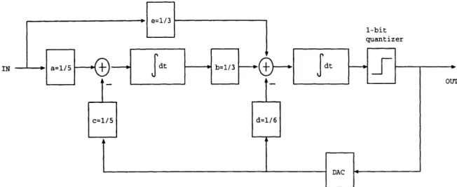
The sigma-delta ADC used in the inertial instrument to convert compensation vari-able signals incorporates the sigma-Delta modulator SD2ADC, a second-order switched-capacitor-based design. This SDM typically runs at a sampling rate of 320KHz and consumes 7mW of power at 5V. Figure 2-1 is a block diagram of the modulator.
Although the SDM is an analog circuit, it operates like a digital circuit and can be analyzed as such. Figure 2-2 is a discrete-time equivalent of Figure 2-1. In this block diagram, the switched-capacitor-based integrators are represented with the ac-cumulator system function G(z) = __. Also, the 1-bit digital-to-analog converter used to feed back the digital output y[n] can be removed since the system is already digital. The gain values a, b, c, d, and e are chosen as such in order to keep the system stable.
e=1/3
1-bit quantizer
IN a=1/5 - dt b=1/3 dt d
§
d=1/6
Figure 2-1: SDM Block Diagram
e [n]
=15G(z) bn G(z)
s[n]= 1-bi
x[n]+t[n] quan izer
c=1/5 d=1/6
2.1.1
Sources of Noise
Quantization Noise
The 1-bit quantizer, which lies at the output of the SDM, produces an output of 2.5V if the input is positive, and -2.5V if it is negative. As shown in Figure 2-2, the effect of the quantizer can be approximated simply as an additive noise sequence e[n]. Typically, given the quantization level A = 5.OV, e[n] can be approximated as a uniformly distributed white-noise sequence, distributed over ± with a probability of A. This distribution is shown by Figure 2-3. The variance of uniformly distributed white noise is calculated as follows:
A 'A2 -2 Te2 de = -=2.0833 (2.1) 2 P (e) 1/5 e -2.50 2.50
Figure 2-3: Distribution of e[n] based on input voltage
In the case of a white noise sequence, its power spectral density (PSD) is constant over all frequency with its magnitude equal to its variance. Thus, for e[n]:
V2
<De(ejw) = 2.0833- (2.2)
rad
In reality, the quantization error sequence e[n] is not exactly a white noise sequence due to the fact that e[n] is correlated with the input x[n]. However, the white noise approximation is made more valid by the fact that other sources of noise in the SDM act as a dither signal that randomizes the input.
Thermal Noise
Because the SD2_ADC is a switched-capacitor-based design, it is also susceptible to thermal noise. According to Norsworthy [3], thermal noise is caused by the random fluctuation of carriers due to thermal energy. Because thermal noise is present even at equilibrium (e.g., in a turned-on MOSFET with zero average current flow), it needs to be taken into account for both the switches and op-amps in a switched-capacitor circuit. Thermal noise can be approximated as having a flat spectrum and a wide band that is limited by the time constants of the switched capacitors (which is determined by the size of the capacitors and the on-resistance of the switches) or the bandwidth of the op-amps. Thermal noise spectrm is flat because it is generally uncorrelated with the input. Because the sampling rate of the circuit is typically lower than the
bandwidth of the thermal noise, the effect of the noise is worsened by aliasing. The thermal noise performance of an SDM is determined mainly by the switch noise and the op-amp noise of the first integrator (that is, the integrator closest to the input) because of the gain this integrator provides for the lower in-band frequencies [3]. Thus, as shown in Figure 2-2, thermal noise can be modeled as additive noise t[n] at the input of the SDM.
As mentioned earlier, thermal noise is generally uncorrelated with the input [2]. Because of this fact, thermal noise can be modeled as a normally distributed band-limited white noise sequence. Previous testing of the SDM indicate that the thermal noise level is approximately -1 1 4dBv 2 1
HZ
Other Sources of Noise
In addition to quantization and thermal noise, there are several other sources of noise in the SDM. They are not considered in the analysis because they are insignificant compared to thermal and quantization noise. Aliasing noise and idle tones are two such sources of noise. Because the input signal is bandlimited by a low-pass filter, the effect of aliasing due to SDM sampling is minimized. In this analysis, this type
of aliasing noise will be simply grouped with thermal noise. Idle tones can become a noticeable noise source in the passband for constant inputs near the rail. Such inputs cause problems because a constant positive input near the rail may produce an output pattern that consists mostly of I's with an occasional, periodic 0, while the converse will occur with a constant negative input. These occasional O's or l's have low periodicity and are reflected as spikes in the passband. In order to avoid this form of noise, the input voltage to the SDM is limited to +2. Thus, this source of noise need not be considered.
2.1.2
Signal and Noise Transfer Functions
The behavior of the SDM is characterized by its signal transfer function (STF) and noise transfer function (NTF). As the name suggests, the STF determines how the input signal x[n] is affected by the modulator, while the NTF determines how the quantization noise sequence, in this case e[n], is shaped. By using superposition, the STF X(z) YN)and the NTF Y E(z) can be determined independently. Based on Figure 2-2,
the STF is determined as follows:
Y(z) = V(z)G(z) (2.3)
V(z) = eX(z) + bG(z)W(z) - dY(z) (2.4)
W(z) = aX(z) - cY(z) (2.5)
which combine to form:
Y(z) _ abG2(z) + eG(z)
(2.6) X(z) - 1+dG(z)+bcG2(z)
Substituting in appropriate values for a, b, c, d, e, and G(z):
2 _ 1-1
STF(z) = 37 - 3 (2.7)
13 Z-1 + Z-2
The NTF of the SDM can be determined similarly. To determine the NTF:
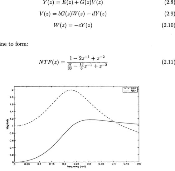
Y(z) = E(z) + G(z)V(z) (2.8)
V(z) = bG(z)W(z) -dY(z) (2.9)
W(z) = -cY(z) (2.10)
which combine to form:
1 - 2z-' + z-2 NTF (z)--7-13 z-1 + z-2 (2.11) TO- 6 2-T 1.8-1.6 - 1.4- 0.8-0.6 0.4- 0.2-0 0.05 0.1 0.15 0.2 0.25 0. 3 0.35 0.4 0.45 0.5 frequency (rad)
Figure 2-4: Signal and noise transfer functions of the SD2_ADC
The frequency characteristics of the STF and the NTF can be examined by re-placing the variable z in Equations 2.7 and 2.11 with ej'. The variable W ranges from 0 to 27r, which is equivalent to 0Hz to the sampling frequency
f,.
Figure 2-4 shows the magnitude response of the STF and the NTF, with the x-axis being the radian frequency w. It can be seen from Figure 2-4 that at low frequencies, the signal x[n] will be minimally affected by the SDM since it is shaped by the STF. However, the quantization noise will be shaped by the NTF such that it is minimized at low frequencies.2.1.3
Performance
The performance of an SDM is typically measured in terms of its signal-to-noise ratio (SNR), a ratio of the signal and the noise power. Before introducing the non-idealities associated with the actual filter used in the Draper Laboratory design, a
100Hz brick-wall low-pass filter can be applied in order to get a good sense of the SDM performance.
In [4], total power in signal g[n], P9 is defined as:
P9 = E(g2[n]) = Ogg [0] = 1
jD.,(eiW)dw
(2.12)where E(g2[n]) is the expected value of g2[n], qgg[r] is the autocorrelation of g[n], and
4bg,(eiw) is the fourier tranform of
#gg
[7]. bgg(eiw) is also the power spectral density(PSD) of the sequence g[n].
In determining the power of the input signal x[n], the signal transfer function of the SDM, STF(ew), and the low-pass filter must also be taken into account.
Px = -Lfw_". (ew) -ISTF(w)|2 dW (2.13)
w, = 27rfcT = 27r(lOOHz)(3 2 KH 0.2rad (2.14)
Some simplifying assumptions can be made with regards to Equation 2.13. In this analysis, the input x[n] is simply a 5Hz, 4V peak-to-peak sinusoid. Thus, the signal is unaffected by the low-pass filter. Also, since the signal is a at relatively low frequency, the STF can be approximated as unity. This simplification makes power easy to determine. If x[n] = 2 cos(t), then using Equation 2.12
Px = E([2cos(t)]2) = 4. E( 1[1 + cos(2t)]) = 2V2 (2.15)
shaped by the noise transfer function rather than the signal transfer function.
Pe = -Lf_', 'De(ew) -INTF(w) 2dw (2.16) = f_"': -(2.0833) - INTF(ew) 2 dw
= 8.62 x 10⁻¹³V2 (2.17)
It can be seen from Equation 2.16 that quantization noise in the low-pass-filtered region is significantly reduced by the noise transfer function. Given the power of the signal and the quantization noise, the SNR of the SDM due to the quantization noise can be determined.
SNRq = 10- log10 (Pi) ~ 123.66dB (2.18)
Pe
Using the definition of effective number of bits (ENOB) described in Section 1.3, 123.66dB translates to approximately 20 bits of resolution. However, thermal noise further limits the effective resolution of the SDM. In fact, because thermal noise is not shaped by the NTF, it could actually be more significant at lower frequencies.
Earlier, the thermal noise level was given as -114 Hz2. The value -114dbV 2 can also
be represented as follows.
-114dB VdB12 = 10. log1o ((V\ 2 V22) (2.19)2.
x = 3.98 x 10~2 V2
bth (f) = 3.98 x 1 0-12V 2 (2.20)
As shown above, the thermal noise level can also be expressed as 3.98 x 10⁻¹²V Hz For a 100Hz band, the resulting thermal noise power is:
Pth = 0 Pth (f)df = 3.98 x 10- _- 100Hz = 3.98 x 10~10V2 (2.21)
resulting in a signal-to-noise ratio of
S NRh = 10 -log y 0 ~ 97.01dB (2.22)
(Pth
This value, which is significantly lower than SNRq, is equivalent to approximately 16 bits of resolution.
These calculations assume an ideal filter in order to focus on the performance of the SDM. In reality, non-idealities associated with the digital filter actually used further limit the achievable resolution. This relationship is examined in later sections.
2.2
Digital Filter
2.2.1
Overview
The output of the SDM represents an oversampled input sequence along with various in- and out-of-band noise. The purpose of the digital filter is to preserve the original input while removing the out-of-band noise. Once the filtering is done, the signal must be downsampled in order to reflect the original input. Insufficient filtering can result in significant noise penalty due to aliasing caused by downsampling.
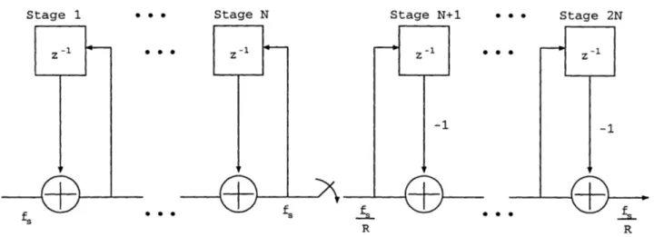
In the Draper sigma-delta ADC design, the architecture used for digital filtering is a finite-input-response (FIR) low-pass filter implentation known as the cascaded integrator-comb (CIC) filter [5]. This implementation is used for two main reasons. First, it has a simple hardware implementation. As mentioned earlier, one of the main design considerations for the Draper sigma-delta ADC is low power consumption. As shown in the next section, the CIC filter is extremely hardware efficient, requiring only adders and registers. Because of its hardware simplicity, it consumes less power than FIR architectures that require multipliers. Second, the filter architecture is such that a separate decimator is not needed. The downsampling rate can simply be specified as a filter parameter.
Integrator Section Stage N Z-1 f fs -.s R Stage N+1 S Z-1 * * -1 * *
Figure 2-5: CIC Filter Block Diagram
2.2.2
Architecture
A block diagram of the CIC decimation filter is shown in Figure 2-5. As the figure shows, the filter is divided into two main sections, the integrator section consisting of a set of N integration stages and the comb (differentiator) section formed by a set of N differentiation stages.
Each integration stage is implemented as a one-pole filter with a unity feedback coefficient. It runs at the high sampling rate of f8, which is the same as the clock rate of the SDM. The system function of each integrator stage is
1
Hi(z) = 1 (2.23)
As seen from Figure 2-5, the comb section receives only every Rt" dati sample from the integrator section. Also, each differentiation stage runs at the downsampled frequency of L. This reduced clock-rate operation of the comb section effectively results in the downsampling of the output data by a factor of R. The system function of a single differentiation stage, relative to the high sample rate
f,
isStage 1 Z-1 fs * S S OSO OSS Stage 2N Z-1 -1 R Comb Section
Hc(z) =1 - z- (2.24) Combining equations 2.23 and 2.24, the system function of the overall filter can be determined.
N N 1 -Z-R )N -1 lN
H(z) = HIN(z)HC = -g-1 = [ -k] (2.25)
( ) k=O
It can be seen from Equation 2.25 that a CIC filter with N stages in each section is essentially an Nth-order FIR filter. The magnitude response of the Nth order CIC filter is as follows.
|H(ejw)I2 _ _ n)N _ 1N N (sin N
(e ± -2j sin t)N 2
~ N
_ (2.26)
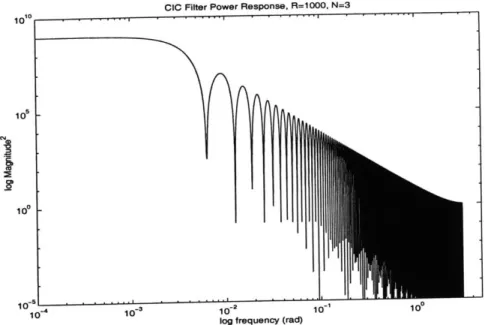
As Equation 2.26 shows, the magnitude response of a CIC filter is approximately equal to an Nh -order sinc function. The shape of the sinc function is dependent solely on the order N and the downsampling rate R. Thus, these variables can be manipulated to provide the desired passband and rolloff characteristics of the filter. Figure 2-6 is an example with N = 3 and R = 1000.
It should be noted that the system functions of the CIC filter shown above apply to the filter operating at the high sample rate
f,.
The operation of the CIC filter can be viewed as a two-step process. First, the SDM data, which is sampled atf,
= 320KHz, is shaped by the function shown in Equation 2.26. The variable W inthis function is calculated relative to the sampling rate of the SDM (the high sample rate). Next, output of the filter is resampled at the low sample rate of L'. This resampled output is the final output of the filter. The effect of decimation, as well as the details regarding the hardware implementation of the filter, are discussed in later sections.
CIC Filter Power Response, R=1000, N=3 1010
10
10-51
-4 2 0
log frequency (rad)
Figure 2-6: Magnitude response of a CIC filter with N=3, R=1000.
2.3
Combined Analysis
In this section, the results of the SDM analysis and the CIC filter analysis will be combined to estimate the performance of the Draper sigma-delta ADC.
2.3.1
Signal and Noise Power
In the case of the ideal 100Hz brickwall filter, the signal remained unchanged, while noise remained only in the passband. However, because the CIC filter exhibits some attenuation in the passband, signal power must be reevaluated. Also, noise must be evaluated over the entire spectrum since out-of-band noise cannot be removed
completely by the CIC filter.
The input signal in this analysis is a
fi,
= 5Hz, 4V peak-to-peak sinusoid. Since all of its power is contained at one frequency, the filtered signal power, P'f, is calculated simply asPxf = Px -jH(ewaig)12 (2.27)
where IH(ej')I is from Equation 2.26. As long as the design of the filter is such that
W,8g is less than the cutoff (-3dB) frequency of the filter, the attenuation of the signal
in the passband is not significant.
Out-of-band quantization noise power is significantly reduced by the CIC filter, but it cannot be completely removed. Power of the shaped quantization noise is calculated as:
Pef = +Jc e(e3) -|NTF(w)12 - H(ejw) dW (2.28)
2,7r - w
While most of Pef comes from the noise in the passband, filtered out-out-band noise covers a wide frequency band and cannot be ignored for several reasons. One is that the out-of-band noise covers a much wider spectrum than the in-band noise. More importantly, the out-of-band noise is shaped by the NTF, which increases according to the order of the SDM at high frequencies. The filter must be good enough to attenuate the rising noise.
It was previously stated that the thermal noise level of the SDM running at 320KHz was - 1 1 4dbv, Hz 7Hzwhich is equal to 3.98 x 10⁻¹²V2 (Equation 2.20). Given this information, the thermal noise PSD in radians, cJth(ejw), and thermal noise power after filtering, Pthf, can be calculated.
foo4 Dth(f)df = ot (2.29)
= (3.98 x 10⁻¹²) -
(
) = 6.368 x 10⁻⁷V2Noting that Dth (eiw) is also constant over the entire spectrum,
2 = _L~T~j'r
=th 2 Jr Dth (ejw)dW (2.30)
4Dth(ejw) = a2 (2.31)
Pthf = -Lf, rIth(ejw) - |STF(w)12 -_IH(ejw)12 dw (2.32)
Equations 2.29 and 2.31 can be found in [6] and [4], respectively. The above equations assume that thermal noise, like quantization noise, is white. While both quantization and thermal noise are approximately white, out-of-band thermal noise
is less significant than quantization noise due to its shaping by the STF rather than the NTF.
Using Equations 2.27, 2.28, and 2.32, the signal-to-noise ratio of the overall SDM can be calculated as:
SNR = 10 - log 0 (2.33)
\Pef + Pthf
(
2.3.2
Downsampling
As mentioned earlier, the CIC filter not only low-pass-filters the signal but also down-samples the output by a factor R relative to the input. In order to prevent the aliasing of the passband that could result from downsampling, R must satisfy the following inequality.
2f >fp b
R < 2 (2.34)
fpb
fpb in the above equation represents the highest frequency in the passband. In the
case of the input signal a~n], fpb can be replaced with
foig
= 5Hz, resulting in the Rnax = 32, 000.Even if R is less than Rmax and the signal in the passband is not aliased, because the CIC filter cannot completely remove out-of-band noise, aliasing of noise outside of the passband cannot be avoided. As a result, the out-of-band noise essentially "folds into" the passband after downsampling, resulting in an increase in the noise level in the passband. However, the total signal and noise power in the spectrum remains unchanged after downsampling. Since the equations in the previous section take into consideration the signal and noise power over the entire spectrum rather than just the passband, the analysis need not be altered.
2.3.3
Obtaining Filter Parameters
Given a desired ADC resolution in terms of ENOB (effective number of bits), the equations for signal and noise power in the previous section can be used to determine the necessary filter parameters. However, because it is exceedingly difficult to come up with a closed form expression to solve for the filter parameters N (filter order) and R (decimation rate) given the ENOB, a Matlab script was created to automate this task. This script, rn-choose.m, can be found in Appendix A.1.
The following parameters are specified in the script. " Desired ENOB
" SDM sampling rate f, * SDM order p
" SDM transfer functions STF(ew) and NTF(ew) " Signal frequency
f
8ig" Quantization noise PSD <I,(ew) =a,. * Thermal noise PSD bIth(e=w) _h
Given this information, the script iteratively produces the CIC filter magnitude re-sponse IH(eiw)l and calculates the values Pj1, Pef, and Pthf in order to determine
the ADC signal-to-noise ratio. As the starting point, the script chooses N = p + 1.
Setting N as such is to ensure that the rolloff of the filter, which is determined by its order, is greater than the rate at which the NTF rises. For each value of N, R starts from 0 and is incremented by 1 until the calculated SNR is high enough to obtain the desired ENOB. In case the given ENOB cannot be achieved due to the limitations of the SDM and the filter, the script also stops running when increasing R lowers the SNR (which would happen when the cutoff frequency of the filter is low enough to severely attenuate the input signal). The script produces matching R values for
N = p+1....-, p + 3. Multiple R-N pairs are obtained in order to find a pair that produces the optimal settling time.
2.4
Results
2.4.1
Filter Parameters
Using the Matlab script rn-choose.m, filter parameters were obtained for ENOB of 14 bits and higher. The resulting filter parameters and the corresponding signal-to-noise ratio are summarized in Table 2.1.
ENOB (bits)
R
SNR (dB) N=3 N=4 N=5 N=3 N=4 N=5 14 243 207 186 86.20 86.21 86.17 15 387 333 300 92.07 92.10 92.11 16 1171 1021 916 98.08 98.09 98.08 17 5587 4875 4381 104.10 104.10 104.10 17.26 (max) 12550 10909 9781 105.66 105.65 105.64Table 2.1: Filter parameters for various ENOB values
As shown in Table 2.1, for a 5Hz input signal, the maximum possible resolution is approximately 17.26 bits according to this analysis. There are two reasons why the ENOB cannot be increased beyond this point. One is that the filter cutoff frequency cannot be less than fig, which results in an unavoidable minimum amount of noise power. The other reason is that the filter's passband gets narrower with increasing R. Since the passband attenuation is greater at higher frequencies, increasing R results in greater input signal attenuation.
The calculations also show that the downsampling rate R increases significantly for each additional bit of resolution, regardless of the choice of N. Thus, this filter architecture, and perhaps the overall ADC design, may not be suitable for achieving a significantly higher resolution.
2.4.2
Multiplexing
Much analysis and calculation were done so far in order to determine what the filter parameter needs to be for a given resolution of the ADC. This data can now be used
multiplexed into one ADC.
In order to determine the optimal rate of switching the multiplexer, the settling time of the ADC must be determined. In this analysis, settling time is defined as the amount of time it takes for the output to reach a steady-state value given a step input. The settling time of the ADC is determined by the settling time of the SDM,
tsdm, and the settling time of the digital filter, tfilt. Because these are the dominant
delays in the ADC circuit, settling time of the ADC is approximately
tadc = tsdm + filt (2.35)
The filter settling time tf il can be determined quite easily. In the case of an FIR filter, the settling time of the filter is simply the amount of time it takes to fill every tap of the filter with new data. That is, when the multiplexer switches the input to the ADC from one source to another, the settling time of the filter is the amount of time it takes for all the taps of the filter to contain a data sample of the new source. Thus, in the case of the CIC filter (or any other FIR filter), the settling time can be regarded as being independent of the inputs being multiplexed. In Equation 2.25, the transfer function of the CIC filter was expressed as a summation notation. This equation can be expanded as such.
H(z) = 1 + aiz-1 + a2z~2 + ... + a(R-1)Nz-(2)36)
As expressed by this equation, a CIC filter with order N and downsampling rate R will have (R - 1)N taps. Given this value, the settling time of such a CIC filter is:
1
tfilt= N (R - 1) - 1 (2.37)
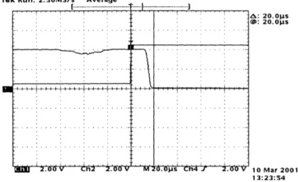
The settling time of the SDM is harder to derive analytically. Thus, the settling time of the SDM was obtained by testing it in the laboratory. The details of the laboratory setup is discussed in a later section. The SDM settling time was estimated by injecting the SDM with a 20Hz, 4V peak-to-peak square wave. Figure 2-7 is a
screen capture of the oscilloscope with this setup. As seen in Figure 2-7, the SDM
Tek Run: 2.50MS/s Average
MM 2.65v L25 2OV M7W2.OJJs 4
A: 20.Opis @D: 20.Ops
2.UV V10Mar 2001 13:23:54
Figure 2-7: Laboratory measurement of SDM settling time
seems to settle approximately 20pus. However, this value is somewhat inaccurate and will be discussed in more detail in Section 3.4.1.
Table 2.2 summarizes the settling times for different ENOBs and filter order. Because the SDM settling time is orders of magnitude smaller than the filter settling time, the values in this table only reflect the filter settling time. As the table shows,
ENOB (bits) Settling time (s)
N=3
N=4 N=5 14 0.0023 0.0026 0.0029 15 0.0036 0.0042 0.0047 16 0.0110 0.0128 0.0143 17 0.0524 0.0609 0.0684 17.26 (max) 0.1176 0.1363 0.1528 Table 2.2: Settling time for various ENOB valuessettling time consistently increases as the filter order goes up. Thus, when optimizing the CIC filter for settling time, the lowest possible order filter should be chosen.
For the application in the inertial instrument, it was desired that four multiplexed inputs be switched at a rate of 20Hz, essentially digitizing each input source at 5Hz. This rate of multiplexing would require the settling time of the ADC to be -O-=
.. . . . . . . . . . . . . . .. . . . .
..
...
..
...
..
...
..
..
..
. . . ... ... .. .. ... ... .. .. .. .. ... .
for upto 16 bits of resolution. For higher resolution, the multiplexer must be switched at a slower rate to avoid error.
2.5
Laboratory Setup and Measurements
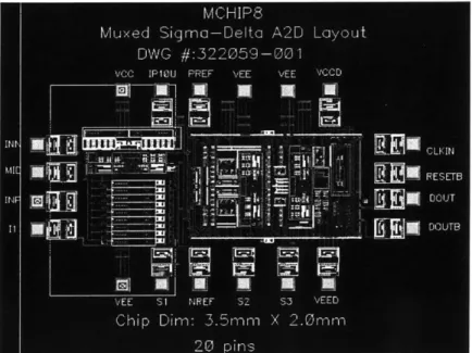
In order to verify the previously measured data and gather new data, various tests were run on the SDM in the laboratory. Due to the lack of availability of the actual inertial instrument electronics, the tests were run on a test chip, shown in Figure 2-8.
Figure 2-8: Layout of the test chip
One of the main difference between the actual SDM chip and the SDM in the analysis is that the actual SDM does not produce output signals ranging from -2.5V to +2.5V but rather produces t2.5V centered around a DC offset of
+2.5V.
This offset, known as MID, can be seen as one of the inputs to the SDM core in Figure ??. Both MID and the reference signal PREF are supplied by the a power source, while the SDM clock was generated by the HP3325B Synthesizer/Function Generator.In order to examine the settling behavior of the SDM, the SDM input was con-nected to a 20Hz, 4V peak-to-peak square wave generated by the HP3325B function generator. The output was viewed with a Tektronix TDS 754D Digital Phosphor
Os-cilloscope. In order to view the settling behavior in the SDM output, the averaging function of the oscilloscope was used. This function reduces random noise in periodic signals by storing the waveforms generated after each trigger event and then display-ing the average of the collected waveforms. Thus, the output of the oscilloscope does
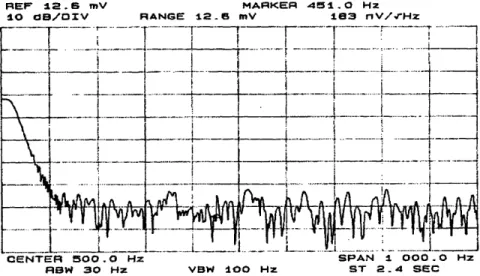
not exhibit any time delays. Figure 2-7 shows the result of averaging 100 samples. Another test of interest was to verify the previously measured thermal noise level of -114dY2 HZ . Because sine waves generated by the function generator HP3325A has a harmonic distortion of upto -65dB relative to the fundamental in the frequency range of interest, the input to the SDM was simply tied to MID for this test. Also, in order to reduce the noise associated with PREF, PREF was first passed through a passive low-pass filter with a cutoff of 1KHz (R = 5KQ, C = 100pF). The output of the SDM was viewed using the spectrum analyzer HP3585B. In order to improve the resolution on the spectrum analyzer, a passive low-pass filter with a 1KHz cutoff (R = 1.5KQ, C = 0.1puF) was used to reduce the noise level in higher frequencies. Figure 2-9 shows the output of the spectrum analyzer.
REF 12.6 mV MARKER 451.0 Hz 10 dB/OIV RANGE 12-6 mV 183 nV/.rHz .-... ...-... .. ...-... 1- ----.
.-
i---
i1
i..._..
---
...
_ _ ..
.L...
CENTER 500.0 Hz SPAN 1 000.0 Hz RBW 30 Hz VBW 100 Hz ST 2-4 SECFigure 2-9: SDM Thermal Noise Plot
The plot shows the thermal noise level to be approximately 180 V Since a 1oX probe was used, this value is actually 1.8--, which is approximately equal to
2
___2
-115dBvy. Hz This value closely matches the previously measured value
2
Chapter 3
Simulation Using Simulink
3.1
Overview
In order to determine the validity and the accuracy of the analysis shown in the previous section, the sigma-delta ADC was simulated using Simulink, a graphical, block-diagram-based tool that facilitates modeling and simulating dynamic systems in Matlab. Simulink was used to simulate the design before implementing and simulating the hardware in VHDL because of its speed and flexibility. The original Simulink model of the overall compensation variable electronics was created by Ed Balboni of Draper Laboratory, and the model was modified in order to focus on the SDM-CIC filter interaction.
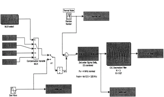
The top-level block diagram of the Simulink ADC model is shown in Figure 3-1. As the figure shows, the model is comprised of the inputs, multiplexer, SDM, CIC filter, a random number generator, and blocks to capture the data at various points of the design. The switch s is used to choose between a single input or a multiplexed input based on the type of simulation. All of these components operate on a common clock running at of 320KHz.
The following sections discuss the implementation of each component in Simulink and the results of simulation.
Corpensaton WriableAD Swimjtion 11heraW os 31 2nd order Sna-Deka sMW Fs =4 MHzwwmW Fsdmn=Ms125= 320Khz sintWe
CIC Decmtn Fier N=3
R=1167
__4
Figure 3-1: Top-level Simulink Model Block Diagram
3.2
Sigma-Delta Modulator
The SDM model created in Simulink is a discrete-time approximation of the actual SDM design. Although it does not exhibit the various non-ideal qualities of an actual SDM, this model does produce realistic quantization noise. Thus, its output is much
more reliable than the white noise approximation used in the previous section. Figure 3-2 is the block diagram of the SDM. In this figure, The quantizer block is followed by a gain of 2.5 in order to simulate a quantization level of 2.5V. The two "stage" blocks are identical except for the inputs they take. Figure 3-3 shows the components of the Stage 2 block.
Each stage associates its inputs with the appropriate gain and integrates them. The discrete-time switched-capactior integrator is simulated by a continuous-time adder with a unit delay in its feedback loop. A saturation block is used to keep the integrator from going above or below ±2.5V.
Figure 3-2: SDM Block Diagram abcd24 In2 abcd2l + Y12 +1-2.5 Ot In3 > Wbc25
Figure 3-3: Details of "Stage 2" of the SDM SDM kn
lnn00
--Stage I
Stage 2
3.2.1
Thermal Noise
As mentioned earlier, this SDM model does not exhibit any non-ideal behavior. Thus it does not include thermal noise, which puts a significant limit on the resolution of the ADC. In order to incorporate thermal noise into this model, a pseudorandom number generator (PRN) block was added to the input of the SDM.
The PRN block used in the model generates a pseudorandom number with a Gaussian distribution on every SDM clock cycle using a table lookup algorithm to generate the output. This algorithm is similar to the Fortran function RNOR de-scribed in [7] but uses a different uniform random number generator to produce the index to the table. The period of this algorithm is much larger than 21, providing suf-ficient randomness even for very long simulations. The mean and the variance of the pseudorandom number sequence was set to 0 and 3.98 x 10⁻¹² -160000 = 6.368 x 10⁻⁷, respectively.
3.3
CIC Filter
The Simulink model of the CIC filter, like the model used in the analysis section, is ideal. As shown in Figure 3-4, ideal delay units are used in the feedback and feed-forward paths instead of the finite number of registers used in the actual hardware. This substitution could mask the potential rounding errors associated with having finite number of registers in the hardware. However, the purpose of this model is to verify the correctness of the analysis in the previous section, which did not take such matters into consideration. Thus, this model is sufficiently accurate.
The registers a, b, and c are clocked at the same rate as the SDM,
f,
= 320KHz, while registers d, e, f, and g are clocked at the downsampled rate of L. Register d in this model essentially acts as the switch shown in Figure 2-5. Since CIC filters have an inherent gain of RN, the gain block G found at the input of the filter reduces the gain by g = g, thus allowing the output magnitude to correctly reflect that of the input.3d order CIC fler
G
p. . dawneaMh by R
ab C +
d
Figure 3-4: Simulink CIC Filter Implementation
3.4
Results
3.4.1
SDM Settling Time
Although an estimate for SDM settling time was obtained in the lab, this value is somewhat unreliable due to the resolution limiation of the instrument used. However, a more accurate settling time value can be obtained through simulation.
It is difficult to measure the settling time of the SDM because it is hard to observe a settling behavior from an output that is strictly digital in the time domain. However, this problem can be remedied by replacing the quantizer with a gain block. Such
replacement is valid since the quantizer does not affect the dynamics of the SDM loop but simply adds noise. This replacement effectively removes the quantization noise, making it possible to observe and measure the settling behavior.
Figure 3-6 shows the settling of the SDM when the input transitions from negative rail to positive rail. Although a quick transition occurs in the output approximately
(6samples) - ( 1second );t~ 19ps after the input transitions from low to high, (sim-ilar to - 20ps observed in the lab), the plot shows that the output oscillates for quite
GD-5DM hn Outi - -t 1n2 Stage I Mn2Outi Sten quantizer replaed by
Figure 3-5: Modified SDM Block Diagram
2 0 -1
4.8 4.801 4.802 4.803 samples~n]
Figure 3-6: SDM Settling Response
SDM Out
SDIF I Iput
SDK Output
4.804 4.805
was found to decay at the rate expressed by Equation 3.1, where
f,
is the sampling rate of the SDM.x(t) = 7.38.- e~0 3 7
f-,(3.1)
This decay is shown in Figure 3-7.
- SDM Output 5----4 - 0-5 10 15 20 25 30 35 40 45 50 samples (n)
Figure 3-7: Decay of the SDM output oscillation
In order to determine the exact settling time of the SDM, it is important to first come up with an accurate definition for the SDM settling time. For this analysis, SDM settling time will be defined as the amount of time it takes for the SDM output to reach a value that is within -- LSB (least-significant-bit) of the output of the2 ADC when the input transitions from negative rail to positive rail. The half-LSB value is calculated as (*sitg" 2 ,iloltage), where Bout is the number of bits at the
ADC output (which is not necessarily ENOB). Using this definition and Equation 3.1, the settling time of the SDM can be estimated for various ADC output widths. Table 3.1 summarizes this information.
In Table 3.1, the upper bound for ADC output width is set rather generously at 30 bits. Thus, this entry is labeled "Max", and the corresponding settling time value will be considered the maximum settling time of the SDM.