Analog-Digital Co-existence in 3D-IC
by
Gilad Yahalom
B.Sc., Technion - Israel Institute of Technology (2008)
S.M., Massachusetts Institute of Technology (2012)
Submitted to the Department of Electrical Engineering and Computer
Science
in partial fulfillment of the requirements for the degree of
Doctor of Philosophy in Electrical Engineering
at the
MASSACHUSETTS INSTITUTE OF TECHNOLOGY
February 2016
c
° Massachusetts Institute of Technology 2016. All rights reserved.
Author . . . .
Department of Electrical Engineering and Computer Science
January 29, 2016
Certified by . . . .
Anantha P. Chandrakasan
Vannevar Bush Professor of Electrical Engineering
Thesis Supervisor
Accepted by . . . .
Leslie A. Kolodziejski
Chair, Department Committee on Graduate Theses
Analog-Digital Co-existence in 3D-IC
by
Gilad Yahalom
Submitted to the Department of Electrical Engineering and Computer Science on January 29, 2016, in partial fulfillment of the
requirements for the degree of
Doctor of Philosophy in Electrical Engineering
Abstract
Ubiquitous mobile communication creates an increasing demand for high data rates, complex modulation schemes and low power design. The cost and performance benefits of conventional lithographic scaling are diminishing as process cost increases exponentially. 3D integration has the potential to keep driving performance forward while keeping cost down. The possibility to integrate separate dies with low-parasitic, dense interconnect and shorter routing provides area and power benefits. However, new challenges must be addressed in order to enable design in this new dimension and provide system level improvements. This thesis explores the impact, challenges and advantages of using 3D integration for combining digital and analog circuits for RF applications.
The use of a vertical solenoid inductor in a Voltage Controlled Oscillator (VCO) is proposed. The inductor design utilizes the through-silicon-vias of the 3D stack as part of its geometry. The solenoid inductor exhibits a 28% larger inductance and a 6 dB higher quality factor compared to a conventional planar inductor occupying the same area. The VCO circuit phase noise is improved by 6 dB and exhibits an improved immunity to coupling from adjacent digital clock lines routed on the bottom tier of the 3D stack.
An efficient hardware implementation is presented for an LTE uplink channel. The proposed design processes input data for cellular transmission. The core of the computation includes a variable-length, high-order, mixed-radix FFT and IFFT blocks. The use of energy efficient circuits and algorithms enables achieving an energy efficiency of up to 95 pJ/Sample and additional power savings of up to 24% for different operation modes.
Both designs are combined along with digital-to-analog conversion to create a partial cellular transmitter in 3D-IC. Highly flexible and configurable design allows for various partitioning of the system. The 3D design has a digital link energy efficiency of up to 0.37 pJ/bit, compared to the 33.3 pJ/bit consumed in a multiple die partitioning and 0.83 pJ/bit for a 2.5D interposer emulated design. The use of the solenoid VCO along with digital-analog partitioning between the die tiers enables high immunity to noise and reduction of spurs at the VCO output.
Thesis Supervisor: Anantha P. Chandrakasan
Acknowledgments
During my time at MIT I had quite a bit of unique and wonderful experiences. Studying under world-renowned professors, hearing lectures from great thinkers, visionaries and leaders, witnessing some quirky and impressive hacks. But the best feature of MIT is its amazing, spectacular collection of individuals. People from all over the world, with a great passion for knowledge, learning and collaboration. People who I could learn so much from and share so much with. I am so grateful that I had the privilege to meet these people and to be part of this vast energetic vibrant MIT community.
First and foremost, I would like to thank and express my deepest appreciation and gratitude to my research advisor Professor Anantha Chandrakasan. His continual guidance and support were invaluable in my journey. Anantha, despite his extremely busy schedule and myriad of responsibilities, always found the time to discuss my research and is always sure to provide a valuable piece of advice. Whenever I needed, Anantha was there with an interesting direction to explore and encouragement on the best way to frame and present my work. I have learned a lot from Anantha’s mentorship and guidance. The wonderful, collaborative atmosphere among the students in Anantha’s lab is a true testament to his leadership and character. Thank you Anantha for having faith in me, supporting my research and enabling me to explore new and uncharted territories.
I would like to thank my committee members, Prof. Hae-Seung (Harry) Lee and Prof. Ruonan Han for their advice, feedback and support. I would also like to thank Prof. Dina Katabi and Prof. Luca Daniel for fruitful discussions and advice which helped shape the direction of my thesis work.
This work could not have been done without the tremendous help, cooperation and generosity of MediaTek Inc. and especially Dr. Alice Wang and Dr. Uming Ko. I would like to thank them profusely for helping define, mold and finance this research and their dedication and commitment. I would also like to thank Hugh Meir, Chang Huang and Maria Lawinson of MediaTek’s Austin TX offices for help in the design and fabrication of the 3D solenoid inductor test chip. Further thanks go to Stacy Ho, CC Hsiao, Susheel Bhalabhadra, Zoran Zvoran and Lubna Ikram at the offices in Woburn MA. Their continuous help and
support in providing feedback and reference designs made it possible to create such a complex and thorough test chip of the 3D LTE transmitter chain.
A special thanks goes out to all the students, postdocs and other members of the extended Anantha group lab. Thanks to Arun Paidimarri, Phillip Nadeau and Nachiket Desai for countless useful discussions and debugging sessions. Many thanks to Dr. Nathan Ickes for help in design and debug of PCBs and test setups. My deep gratitude goes out to Mehul Tikekar for helping me in promoting and creating the new Anantha group Wiki and repository, and for being my on-call Unix and Git guru. Many thanks also go out to Avishek, Bonnie, Chiraag, Chu, Dina, Frank, Georgios, Ishwarya, Michael, Mohamed, Omid, Preet, Priyanka, Rahul, Sirma, Sungjae, Utsav and Yildiz for being such a great and supportive group, making it a delight to come every day to the lab. A special warm thank you also goes out to Margaret Flaherty, our group’s administrator, which skillfully coordinates and manages all the workings of the lab and makes sure everything is operating smoothly and efficiently.
Many other great friends and colleagues also deserve recognition. Radhika, Zhipeng, Yan and SungWon, as well as other students in Prof. Weinstein, Sodini and Lee groups. Sunghyun Park was a close companion in the design of the first 3D test chip and helped on many of the initial trouble-shooting of the layout and fabrication at MediaTek.
This work was carried out both at MediaTek as well as the Microsystems Technology Laboratory at MIT, and I would like to thank Michael Mcllarath for assisting with CAD tool support and setup, Mike Hobbs for assistance with IT and computing resources and Deborah Hodges-Pabon for making MTL such a warm and inviting home to all students, faculty and staff. On the administrative side I am most grateful to Janet Fischer, Alicia Duarte and the rest of the EECS HQ members for being so helpful in assisting in all administrative and pedagogical matters.
Aside from the vast amount of people, which only few of them were mentioned above, and helped further my academic research, others here at MIT helped balance out my day and maintain a semblance of normality. Thank you Sarit and Yair, Noa and Jonathan, Inbal and Roy for being fantastic friends and companions. Thanks for endless hours of card games and countless Friday night dinners. Thanks for hikes, road trips, movie nights and
the occasional award ceremony viewing parties.
Although physically far away, my parents’ support helped fuel this long and arduous journey. I know that without the education and values instilled from an early age I would never have embarked on such a journey to begin with. Thank you Mom and Dad for always being there for me.
Lastly, but definitely not least, my biggest thanks, devotion and appreciation go out to my one true friend and soul-mate. My courageous, patient, loving and thoughtful wife Emanuel. All my accomplishments are made possible by her. She makes everything clear and focused and helps put everything in to the right perspective. I would be lost in a vast sea of incomprehensibility without you. Thank you for being by my side always. I love you with all my heart.
Contents
List of Figures 13 List of Tables 19 List of Acronyms 21 1 Introduction 27 1.1 Motivation . . . 271.2 Three Dimensional Integration . . . 28
1.3 Previous work on 3D-IC . . . 33
1.4 Thesis Contributions and Outline . . . 35
2 Passive Structures 41 2.1 Introduction . . . 41 2.2 Analog-Digital Integration . . . 43 2.2.1 Noise Contributors . . . 43 2.2.2 Isolation Techniques . . . 44 2.2.3 Isolation in 3D-IC . . . 46
2.3 Test Chip Design . . . 47
2.3.1 3D Stacking . . . 47
2.3.2 Inductor Design . . . 48
2.3.3 VCO Design . . . 51
2.3.4 Clock Lines . . . 53
2.3.6 Coupling Transfer Function Calculation . . . 59
2.4 Measurements . . . 61
2.5 Conclusion . . . 69
3 Data-Dependent Signal Processing 71 3.1 Introduction . . . 71 3.2 LTE . . . 72 3.3 FFT Overview . . . 78 3.3.1 FFT Algorithm . . . 79 3.3.2 General Radix FFT . . . 81 3.3.3 Bit Reversal . . . 87 3.3.4 Hardware Implementation . . . 88
3.4 Digital Baseband Implementation . . . 97
3.4.1 Hardware Efficient Processing . . . 100
3.4.2 QAM Mapping . . . 102 3.4.3 DFT . . . 104 3.4.3.1 Butterfly Structure . . . 105 3.4.3.2 Delay Lines . . . 107 3.4.3.3 Memory Sharing . . . 109 3.4.3.4 CORDIC Rotation . . . 112 3.4.3.5 Angle Generation . . . 116 3.4.3.6 Index Counter . . . 117 3.4.4 Resource Mapping . . . 119 3.4.4.1 Interpolation . . . 120 3.4.4.2 Transform Decomposition . . . 124 3.4.5 IDFT . . . 126
3.4.6 Cyclic Prefix Addition . . . 127
3.4.7 Upsampling . . . 128
3.4.8 Snapshot Memory . . . 137
3.5.1 Data Path . . . 139 3.5.2 Power . . . 144 3.5.3 Comparison . . . 149 3.6 Conclusion . . . 150 4 Analog-Digital 3D Integration 153 4.1 Introduction . . . 153
4.2 Transmitter Chain Design . . . 154
4.2.1 Chip Layout and Partitioning . . . 155
4.2.2 Digital Baseband . . . 164
4.2.3 Digital Buffering and Level Shifting . . . 165
4.2.4 Clock Distribution . . . 167
4.2.5 Digital Routing . . . 171
4.2.6 Analog Routing . . . 173
4.2.7 Digital to Analog Conversion . . . 176
4.2.8 LO Generation . . . 178 4.2.9 Upconversion . . . 180 4.2.10 Bias . . . 182 4.2.11 External I/O . . . 183 4.3 Measurements . . . 186 4.3.1 Digital Baseband . . . 187 4.3.2 DAC . . . 187 4.3.3 VCO . . . 191 4.3.4 Mixer . . . 192 4.3.5 System Partitioning . . . 194 4.4 Conclusions . . . 198
5 Conclusion and Future Directions 201 5.1 Summary of Contributions . . . 202
5.1.1 Passive Devices in 3D-IC . . . 202
5.1.3 Analog-Digital 3D Integration . . . 204
5.2 Future Directions . . . 206
5.2.1 Full Transceiver Design . . . 206
5.2.2 Power Generation in 3D-IC . . . 208
5.2.3 Heterogeneous Integration . . . 209
A QAM Mapping 211 B Configuration 215 B.1 Scan Chain Architecture . . . 215
B.2 3D Scan Chain . . . 216
B.3 Configuration Options . . . 219
List of Figures
1-1 Peak data rates for various wireless communication standards . . . 28 1-2 (a) Gate count and wafer cost per technology node leading to trend change
in (b) cost per gate . . . 29 1-3 Illustration of different stacking approaches (not to scale) (a) Interposer
stacking (2.5D), (b) 3D stack using F2F and (c) 3D stack using B2F assembly 32
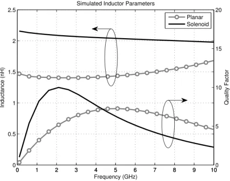
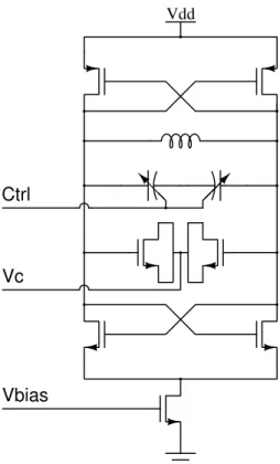
2-1 Illustration of Back-to-Face 3D die stack (not to scale) . . . 47 2-2 3D-IC stack illustration . . . 48 2-3 Monolithic integrated inductor equivalent circuit model . . . 50 2-4 Simulated inductor parameters extracted from field solver simulation results 51 2-5 CMOS VCO core schematic used with both the planar and solenoid inductor
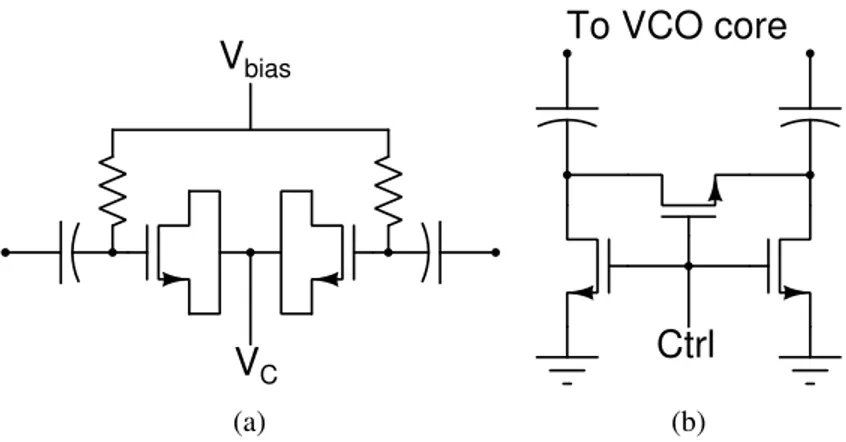
structures . . . 52 2-6 Frequency tuning of VCO achieved via (a) continuous MOS varactor and
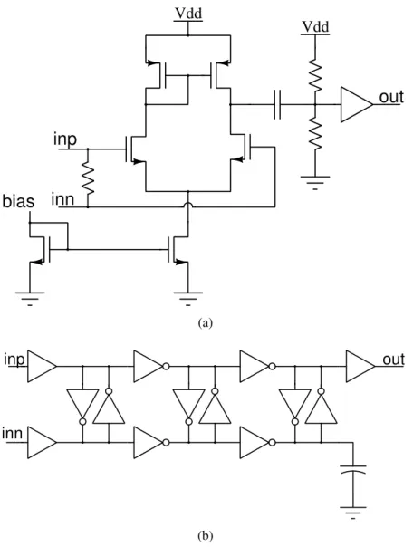
(b) switched capacitor bank unit cell . . . 53 2-7 Differential capacitive divider source follower output buffer schematic . . . 54 2-8 Clock input buffer (a) differential amplifier and (b) pseudo differential
buffer chain schematics . . . 55 2-9 Clock divide by 16 circuit schematic . . . 55 2-10 Controllable clock lines location relative to inductors’ dimension and schematic
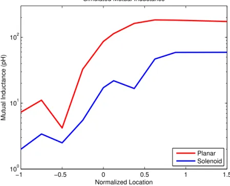
of line switch control . . . 56 2-11 Simulated mutual inductance between clock lines and inductor structures
as a function of normalized clock line offset location . . . 57 2-12 Simplified coupling model between clock lines and VCO LC tank . . . 58
2-13 Die micrograph (a) top tier (b) bottom tier . . . 61
2-14 PCB used for testing and measurements . . . 62
2-15 Measured tuning range for planar and solenoid VCOs . . . 63
2-16 Measured phase noise of planar and solenoid VCOs . . . 64
2-17 VCO output power spectral density with spurious tones caused by coupling from digital clock lines . . . 65
2-18 Clock signal spur power as a function of relative frequency to VCO free-running frequency . . . 65
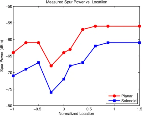
2-19 Clock signal spur power as a function of clock line location . . . 66
2-20 Clock signal spur power as a function of coupling strength . . . 67
2-21 Clock signal spur power vs. aggregate coupling strength . . . 68
2-22 Phase noise measurement with noise coupling from a 1 MHz clock signal . 69 2-23 Output power spectral density of VCO with close-in clock line noise. Planar inductor VCO exhibits injection locking to the clock signal . . . 70
3-1 LTE FDD frame structure . . . 73
3-2 Time domain slot structure with (a) normal and (b) extended cyclic prefix addition to SC-FDMA symbols . . . 74
3-3 LTE uplink (a) resource grid and (b) channel configuration illustration . . . 75
3-4 LTE PHY layer . . . 77
3-5 (a) Localized and (b) Interleaved SC-FDMA subcarrier mapping . . . 79
3-6 Radix-2 decimation in frequency FFT . . . 82
3-7 Radix-2 butterfly . . . 83
3-8 Radix-3 butterfly structure . . . 84
3-9 Radix-5 butterfly structure . . . 85
3-10 Radix-4 butterfly structure . . . 86
3-11 FFT memory architecture block diagram . . . 90
3-12 FFT pipeline architecture block diagram . . . 90
3-13 R2MDC block diagram for 16 point FFT . . . 91
3-15 Radix 2 type I butterfly . . . 92
3-16 R4SDF block diagram for 16 point FFT . . . 92
3-17 R4MDC block diagram for 16 point FFT . . . 93
3-18 R4SDC block diagram for 16 point FFT . . . 93
3-19 Radix 2 (a) type II butterfly and (b) 90◦rotation block diagrams . . . 94
3-20 R22SDF block diagram for 16 point FFT . . . 94
3-21 Radix 2 (a) type III butterfly and (b) 45◦rotation block diagrams . . . 95
3-22 R23SDF block diagram for 64 point FFT . . . 95
3-23 Baseband block simplified architecture . . . 97
3-24 Double buffer handshake process (a) simplified schematic and (b) timing diagram . . . 99
3-25 Constellation mapping block diagram . . . 104
3-26 Variable size UL LTE DFT pipeline topology . . . 106
3-27 Control signal timing for (a) radix-2, (b) radix-3 and (c) radix-5 butterflies with a delay of Tdelayclock cycles . . . 106
3-28 SRAM based delay line schematic . . . 108
3-29 Latch based memory schematic . . . 109
3-30 CORDIC block schematic . . . 115
3-31 CORDIC schematic of (a) quadrant rotator and (b) micro-rotator block . . . 116
3-32 Angle generation for CORDIC following (a) general radix butterfly and (b) simplified architecture for radix 23butterfly block . . . 117
3-33 Mixed radix reverse digit counter for DFT output indexing . . . 118
3-34 Simplified multiplier blocks for (a) 2 bit and (b) 3 bit multipliers . . . 119
3-35 Block diagram of filter re-sampling by a factor of N/M . . . 122
3-36 Reconstructed samples from resampling filter with length (a) L = 12801 and (b) L = 128001 . . . 123
3-37 EVM of reconstructed samples as a function of resampling filter length. 10 sets of 1200 random 64-QAM points using a 2048 point IDFT . . . 123
3-38 Transform decomposition procedure for an FFT calculation with a subset of the inputs . . . 125
3-39 Fraction of operations required in TD-FFT as a function of non-zero sample
ratio . . . 126
3-40 IDFT block architecture . . . 127
3-41 Zero order hold impulse response in the (a) time and (b) frequency domain . 129 3-42 Power spectrum of 10 MHz channel LTE signal in (a) baseband) and (b) at RF around a 2 GHz carrier, with ZOH D/A with no oversampling . . . 130
3-43 Power spectrum of 10 MHz channel LTE signal in (a) baseband) and (b) at RF around a 2 GHz carrier, with ZOH D/A with x8 oversampling and interpolation . . . 132
3-44 Integer rate conversion upsampling system . . . 133
3-45 Low pass interpolation FIR filter (a) time and (b) frequency response . . . . 133
3-46 N tap FIR segment . . . 134
3-47 Expander filter Noble identity . . . 135
3-48 Polyphase decomposition for an interpolating filter using the Noble identity 136 3-49 Polyphase implementation of the x8 interpolation filter . . . 137
3-50 Micrograph of (a) chip and (b) zoom-in of implemented LTE digital baseband chip . . . 138
3-51 Measured 480 64-QAM modulated input symbols . . . 139
3-52 FFT output symbol index . . . 140
3-53 FFT output after zero padding (a) w/o and (b) w/ the use of transform decomposition . . . 141
3-54 IFFT output symbol index . . . 142
3-55 IFFT output power spectral density . . . 142
3-56 Interpolator output power spectral density . . . 143
3-57 Internal trigger signals (a) w/o and (b) w/ the use of transform decomposition144 3-58 FFT block power consumption (a) all FFT sizes and (b) separated into homogeneous radix butterfly blocks . . . 146
3-59 Relative total power when using transform decomposition as a function of FFT size (i.e. number of non-zero samples at input) . . . 147
4-1 Partial transmitter chain block diagram . . . 154
4-2 Schematic illustration of 3D-IC packaging process (dimensions not to scale) 156 4-3 Block diagram of single cube tier in 3D stack . . . 157
4-4 Single die, SoC-like operation emulation (only top tier of cube shown) . . . 158
4-5 Two dies, partition at (a) digital boundary and (b) analog boundary (only top tier of cubes shown) . . . 160
4-6 2.5D operation emulation with partitioning at (a) digital boundary and (b) analog boundary . . . 161
4-7 3D-IC operation with partitioning at (a) digital boundary and (b) analog boundary . . . 162
4-8 Schematic of (a) tri-state buffer and (b) scalable controlled buffer . . . 166
4-9 High-VDD to low-VDD level shifter schematic using thick-oxide inverter cell . . . 166
4-10 Low-VDD to high-VDD level shifter schematic . . . 167
4-11 Clock input differential amplifier schematic . . . 168
4-12 Clock divider schematic . . . 168
4-13 Clock distribution for (a) single and (b) two cube operation . . . 170
4-14 Clock generation and distribution block diagram for two tiers in 3D-IC . . . 171
4-15 Digital crossbar (a) Tx column and (b) Rx column . . . 172
4-16 Digital signal multiplexing block diagram . . . 173
4-17 Analog crossbar schematic . . . 174
4-18 Voltage-to-Current conversion and signal multiplexing schematic . . . 175
4-19 Analog signal path multiplexing block diagram . . . 176
4-20 General schematic of binary-unary current steering DAC segmentation topology177 4-21 DAC data and clock synchronization schematic . . . 177
4-22 First-order, adjustable low-pass filter schematic . . . 178
4-23 Quadrature VCO core schematic . . . 179
4-24 VCO differential buffer driver schematic . . . 180
4-25 Simplified RF mixing DAC schematic . . . 181
4-27 High-speed I/O (a) serializer and (b) deserializer schematics . . . 185
4-28 Micrograph of test chip (same layout used for both top and bottom tiers) . . 187
4-29 DAC voltage output for 11 bit codeword input . . . 188
4-30 Calculated DAC (a) DNL and (b) INL . . . 189
4-31 DAC output spectrum for 5 MHz BW LTE signal . . . 190
4-32 VCO frequency tuning range . . . 191
4-33 Measured VCO phase noise for Planar and Solenoid inductor structures . . 192
4-34 Example of time domain output of solenoid quadrature VCO . . . 193
4-35 Phase difference between VCO quadrature outputs . . . 193
4-36 External mixer output spectrum of 5 MHz BW LTE signal . . . 195
4-37 Digital link power consumption comparison . . . 196
4-38 VCO output spectrum using different partitioning schemes . . . 198
B-1 Scan chain unit cell for (a) writing configuration bits and (b) reading chip data . . . 215
B-2 Scan chain topology for 3D test chip . . . 217
List of Tables
1.1 Summary of Select Previous Work on 3D-IC . . . 39
2.1 Summary and comparison of results . . . 64
3.1 Transmitter available resource blocks for different channel bandwidths . . . 74
3.2 Radix-2 FFT output bit reversal . . . 87
3.3 Mixed radix digit reversal example . . . 89
3.4 Pipeline FFT architecture resource comparison . . . 96
3.5 Valid DFT sizes for LTE UL symbol generation . . . 105
3.6 FFT butterfly memory requirements . . . 111
3.7 FFT memory bank size and grouping . . . 113
3.8 Design Specification Summary . . . 139
3.9 Power and energy consumption summary . . . 149
3.10 Comparison to other LTE OFDMA signal generation processors . . . 151
4.1 System partitioning summary . . . 163
4.2 DAC specification summary . . . 188
4.3 Summary of VCO performance . . . 194
A.1 BPSK modulation mapping . . . 211
A.2 QPSK modulation mapping . . . 212
A.3 16-QAM modulation mapping . . . 212
A.4 64-QAM modulation mapping . . . 213
B.2 General configuration bits . . . 219
B.3 Baseband module configuration bits . . . 221
B.4 DAC module configuration bits . . . 226
B.5 VCO module configuration bits . . . 227
B.6 Mixer module configuration bits . . . 227
B.7 Bias module configuration bits . . . 228
List of Acronyms
3D-IC Three Dimensional Integrated Circuits
3GPP 3rd Generation Partnership Project
AC Alternating Current
ACLR Adjacent Channel Leakage Ratio
ADC Analog to Digital Converter
AMPS Advanced Mobile Phone System
ASIC Application Specific IC
B2B Back-to-Back
B2F Back-to-Face
BEOL Back End Of Line
BPSK Binary Phase Shift Keying
BS Base Station
BW Bandwidth
C4 Controlled Collapse Chip Connection
CAD Computer Aided Design
CORDIC COordinate Rotation Digital Computer
CP Cyclic Prefix
CPU Central Processing Unit
CSD Canonical Signed Digit
DAC Digital to Analog Converter
DC Direct Current
DDR Double Data Rate
DFT Discrete Fourier Transform
DL Downlink
DMIPS Dhrystone Million Instructions Per Second
DRAM Dynamic RAM
DNL Differential Non-Linearity
DSP Digital Signal Processing
DVFS Dynamic Voltage-Frequency Scaling
EDGE Enhanced Data Rates for GSM Evolution
EM Electro-magnetic
ESD Electrostatic Discharge
E-UTRA Evolved Universal Terrestrial Radio Access
EVM Error Vector Magnitude
F2F Face-to-Face
FDMA Frequency Division Multiple Access
FEC Forward Error Correction
FEOL Front End Of Line
FF Flip Flop
FFT Fast Fourier Transform
FIR Finite Impulse Response
FOM Figure of Merit
FPGA Field Programmable Gate Array
GPIO General Purpose I/O
GPS Global Positioning System
GSM Global System for Mobile Communications
HSPA High Speed Packet Access
IC Integrated Circuit
ICI Inter-Carrier Interference
IDFT Inverse Discrete Fourier Transform
IF Intermediate Frequency
IFDMA Interleaved FDMA
IFFT Inverse Fast Fourier Transform
IIR Infinite Impulse Response
INL Integral Non-Linearity
IoT Internet of Things
ISI Inter-Symbol Interference
ISM Industrial, Scientific and Medical
KVL Kirchhoff’s Voltage Law
LDO Low Dropout Regulator
LFDMA Localized FDMA
LNA Low Noise Amplifier
LO Local Oscillator
LPF Low Pass Filter
LSB Least Significant Bit
LTE Long Term Evolution
LTE-A LTE Advanced
MCM Multi-Chip Module
MEMS Micro-Electro-Mechanical System
MIMO Multiple Input Multiple Output
MOM Metal-Oxide-Metal
MOS Metal-Oxide-Semiconductor
MSB Most Significant Bit
MU-MIMO Multi-User MIMO
NMOS N-type MOS
OFDM Orthogonal Frequency Division Multiplex
OFDMA Orthogonal Frequency Division Multiple Access
OpAmp Operational Amplifier
PA Power Amplifier
PAPR Peak to Average Power Ratio
PC Personal Computer
PCB Printed Circuit Board
PE Processing Element
PHY Physical Layer
PLL Phase Lock Loop
PMOS P-type MOS
PUSCH Physical Uplink Shared Channel
QAM Quadrature Amplitude Modulation
QFN Quad Flat No-leads
QPSK Quadrature Phase Shift Keying
R2MDC Radix-2 Multi-path Delay Commutator
R2SDF Radix-2 Single-path Delay Feedback
R22SDF Radix-22Single-path Delay Feedback
R23SDF Radix-23Single-path Delay Feedback
R4MDC Radix-4 Multi-path Delay Commutator
R4SDF Radix-4 Single-path Delay Feedback
RAM Random Access Memory
RB Resource Block
RF Radio Frequency
SC Subcarrier
SDF Serial Delay Feedback
SC-FDMA Single Carrier Frequency Division Multiple Access
SerDes Serializer/Deserializer
SiP System in Package
SoC System on Chip
SRAM Static Random Access Memory
TCAM Ternary Content-Addressable Memory
TD Transform Decomposition
TDD Time Division Duplexing
TSV Through Silicon Via
UE User Equipment
UL Uplink
UMTS Universal Mobile Telecommunication System
VCO Voltage Controlled Oscillator
Chapter 1
Introduction
1.1
Motivation
The development of integrated circuits has allowed for the proliferation of powerful personal computing and communication solutions. The prediction (or observation) set forth by Gordon Moore that the transistor density will double every 18 months [1] proved to be both quite accurate and a major force in driving this revolution. Cellular and wireless communication today is ubiquitous and albeit its relative short history it’s hard to imagine our lives today without being continuously connected to one another.
Along with the advancement in lithographic scaling of integrated circuits, the demand for increased data rate and lower latency increased tremendously as well. From humble beginnings of the analog cellular network at 1984 in the form of the Advanced Mobile Phone System (AMPS), where peak data rates were a mere 14.4 Kb/s [2], the evolution of cellular and wireless communication took on exponential form, much like the growth in semiconductor technology. Fig. 1-1 plots the peak Downlink (DL) data rates for various cellular and wireless communication protocols throughout history. We see that today, current standards such as LTE Advanced (LTE-A) and WiFI 802.11ad call for data rates in the range of a few Gb/s.
However, evidence from recent years suggest that the trends of semiconductor scaling can no longer keep up with such a demanding scaling rate. Most importantly, it may not be economically beneficial to do so even if the technological obstacles can be overcome. Fig.
1980 1985 1990 1995 2000 2005 2010 2015 104 105 106 107 108 109 1010 Year
Peak DL Rate (bit/s)
AMPS 3GPP 3GPP2 IEEE
Figure 1-1: Peak data rates for various wireless communication standards. Reproduced using data from [3]
1-2a plots the cost per wafer for different technology nodes along with the amount of usable transistors per wafer due to reduced yield and effective usable area. While the amount of fabricated gates rises as the feature dimension becomes smaller, issues such as defect density, leakage, doping uniformity, line edge roughness and other physical parameters which are sensitive to minute variation reduce the amount of actual usable gates in the fabrication process. The cost per wafer continues to rise sharply, but the amount of usable devices does not scale as fast. As a result, as can be seen in Fig. 1-2b, the price per transistor is not scaling as it used to in the past. And according to some estimations might even be reversing the trend, making it impractical to continue the strive for further scaling of the process node below 22nm [4].
1.2
Three Dimensional Integration
An alternative to further process scaling is functional diversification. By adding higher degrees of functionality and achieving more diverse integrated systems we can overcome this bottleneck and continue pushing the performance envelope further out. One of the key areas which can enable this approach is 3D packaging. Three Dimensional Integrated Circuits (3D-IC) are an emerging solution to achieve higher functionality diversification in
90 65 40 28 20 14 0 2000 4000 6000 8000 10000 12000 14000 Process Node (nm) Gates/mm 2 (KU) 1200 1700 2200 2700 3200 3700 4200 4700 Cost/Wafer ($) Actual Gates/mm2 Total Gates/mm2 Cost/Wafer (a) 90 65 40 28 20 14 0 0.005 0.01 0.015 0.02 0.025 0.03 0.035 0.04 0.045 Process Node (nm) Cost/M Gates ($) (b)
Figure 1-2: (a) Gate count and wafer cost per technology node leading to trend change in (b) cost per gate. Reproduced from data by [4]
integrated circuits [5].
3D-IC is a relatively new technique, and as such it does not refer to any one specific type of processing, but rather to a broader set of packaging and post-processing techniques used [6, 7]. In general, it is customary to distinguish between package level technologies and technologies which include the use of Through Silicon Vias (TSVs). In package level technologies, which combine several dies in a single package (also known as System in Package (SiP) or Multi-Chip Module (MCM)), the connections are made at the package level interconnect, such as wirebonds and flip-chip bumps (also known as Controlled Collapse Chip Connection (C4)), resulting in connections on the order of a few hundreds of micrometers. Use of TSV technology allows connecting of several dies to a common passive silicon interposer substrate (usually referred to as “2.5D integration”) or vertically stacking several dies. This interconnect level may be below ten micrometers in size resulting in highly dense, low-parasitic interconnect. As the technology matures, we will expect to see the TSV diameter and pitch shrink to the size of a mere few micrometers [8].
Even within the vertical “True 3D” integration process family one may find a myriad of different approaches and variants. In one approach, the dies are fabricated separately, the wafer of one tier is thinned before inserting the TSVs, and only then are the tiers stacked. In another approach, the tiers are grown one on top of each other, creating a new active silicon layer on top of a formed wafer. This allows for denser interconnect and avoids the processing and handling of the thinned wafer. The former approach may be viewed as a parallel manufacturing process resulting in a polylithic structure, while the latter is a sequential process, resulting in a monolithic structure.
Further differences are found at the direction of the die stacking. Whether two adjacent dies will be stacked Face-to-Face (F2F), through micro-bumps, where the top metal layer of each die is connected to the other, and the signals are routed outside of the die stack using TSVs. Or alternatively Back-to-Back (B2B) connection, through the back side silicon substrate of each die or alternatively connected Back-to-Face (B2F). Each connection style entails different constraints over connection size, pitch, density, impact on available active die area as well as the scalability of the connection [9].
die-to-wafer or die-to-die. Again, each choice results in a different trade-off in the manufacturing process which affects yield, testability and flexibility. The TSVs themselves may be added at different points in the fabrication process, dubbed via-first, via-middle and via-last. This pertains to the step in the fabrication process when the TSVs are inserted. Via-first adds the TSVs before the Front End Of Line (FEOL) step and the addition of active devices, via-middle adds the TSVs between the FEOL and Back End Of Line (BEOL) steps. This is the most common approach since it usually gives the best trade-off in terms of cost, yield and manufacturing complexity. The via-last option adds the TSV structures after the BEOL step has completed and all metal routing layers were formed on top of the active die area. Figure 1-3 illustrates schematically a few of the aforementioned techniques and approaches to 3D-IC integration. The figure only illustrates a few representative scenarios for illustration purposes, and only depicts two tier die stacking. The above mentioned 3D stacking techniques are also utilized to stack a larger number of die tiers (as much as 32 in some cases [10]).
Apart from the up-front reduction in foot-print area of the 3D stack compared to conventional planar 2D dies, 3D-IC offers a great advantage in reduced interconnect length which may dominate the chip’s power consumption [11, 12], limit its clock frequency [13] and incur area overhead [14].
Three dimensional integration further opens up the possibility for closely integrating units specialized for different functionalities. This leads to heterogeneous integration, either in the sense of different functionality, different process nodes or completely different materials. Such examples include integrating logic with memory [15–17], optics [18– 20], Micro-Electro-Mechanical System (MEMS) [21–23], power [24, 25], as well as III-V materials with Si [26,27] and so forth. The close vertical integration of active silicon layers gives the designer a new degree of freedom in the system and block level partitioning [28, 29] which enables new architectures for both traditional logic blocks [30], and more complex systems such as Network on Chip (NoC) [31, 32] and Field Programmable Gate Arrays (FPGAs) [33, 34].
Along with these opportunities and advantages 3D integration introduces new challenges [35]. Some of these challenges stem from the new processing techniques required to
FEOL BEOL Si Package FEOL BEOL Si FEOL Die 1 Interposer C4 Bumps µ-Bumps Die 2 TSV Thin Si BGA Bumps (a) FEOL BEOL Package FEOL BEOL Si Die 1 C4 Bumps TSV Die 2 µ-Bumps Thin Si BGA Bumps (b) FEOL BEOL Package FEOL BEOL Si Die 1 C4 Bumps TSV Die 2 µ-Bumps Thin Si BGA Bumps (c)
Figure 1-3: Illustration of different stacking approaches (not to scale) (a) Interposer stacking (2.5D), (b) 3D stack using F2F and (c) 3D stack using B2F assembly
correctly create the die stacks with acceptable yield [36, 37]. The stacking of dies can create thermal hot-spots which might degrade performance. The TSVs and back-grinding of the silicon wafer can cause mechanical stresses and local variation of device parameters [38–44]. Coupling of TSVs amongst each other [45–47] and to substrate [48–50] as well as capacitive and inductive coupling between the two dies [51, 52] may give rise to power and signal integrity issues [53, 54]. Furthermore, reliability and yield might increase overall cost [55–57]. Adding to these issues is the increased complexity of testing [58], as well as relatively new and immature Computer Aided Design (CAD) tools and software for design and validation [59–62].
1.3
Previous work on 3D-IC
There is abundant research on improvement in timing and power for digital systems due to shortened interconnect [28, 63–65], as well as achieving higher system level performance. Such improvements were shown through architectural re-partitioning of digital blocks [66– 68]. Integration of different functional blocks in a 3D stack also shows great potential as seen in examples of integrating digital logic and memory. Below is a partial review of notable recent work which has a greater focus on the circuit and system level potential and challenges of 3D-IC design.
As early as 2004 there has been research carried out by Intel corp. to explore the potential benefits of 3D die stacking for improved system performance in microprocessor design. These initial studies, exploring re-partitioning of deeply pipelined IA32 microprocessors have shown the potential to gain improvements on the order of 15% while reducing power by 15% due to the potential shortening of critical paths and reduced clock routing [66]. Further research focused on integration of logic and memory, combining a multi-core die with an SRAM memory chip to achieve a very high speed interconnect of 1.62 terabits/s and 3x reduction of off-die memory [69].
Professor Eby Friedman’s group at Rochester university has been exploring three dimensional integrated circuits for over a decade and have made significant contributions to the field. Among the circuit level exploration, they have demonstrated the use of distributed transmission
lines in a 3D stack to be used as the inductive element in a DC-DC buck converter, enabling reduction of required capacitor size [70]. This technique allows integration of the power control and generation modules on die without the need for external energy storage components. Also explored were architectures for 3D NoC, analyzing the different trade-offs involved and demonstrating a potential of up to 33% performance improvement over 2D NoCs [31] and designs with 12.8 Gb/s bandwidth and down to 0.9 pJ/bit I/O link power efficiency [71]. Two additional topics explored, which have a tight connection to the proposed research are clock distribution topologies in 3D-IC and power distribution and integrity issues. Their research analyzes the impacts of clock tree topology on metrics such as clock frequency, skew, delay and power dissipation [29]. Similarly, they have shown the impact of different power routing topologies on the overall power delivery response of the design [72]. Others have shown potential for power supply integration and routing in 3D demonstrating such benefits as 45% reduction in DC noise and 65% reduction in overhead power consumed by power supply [73], 13.3% reduction in dynamic noise [74] and 12% improvement in power efficiency when using interposer thick metal lines [25].
Davis et. al demonstrated the potential benefits of re-partitioning conventional 2D circuits in a 3D topology. They showed that by re-designing the circuit architecture across several die tiers, splitting functionality and memory between them they are able to show power and performance benefits. Such improvements include a 22% reduction in cycle-time and 18% reduction in energy/FFT for an 8192 point FFT processor [75] and a 23% power reduction for a Ternary Content-Addressable Memory (TCAM) implementation [67]. Other similar circuit re-partitioning research has shown 16% reduction in delay time for a 3D floating point adder [30], as well as 2x speed improvement and 2.8x reduced interconnect in 3D tree-based FPGA design [34] compared to their 2D counterparts. These results are mainly driven as explained previously by the possibility to significantly reduce the circuit interconnect length in the 3D stack, which can be reduced by up to 51% [76].
Implementing the concepts previously discussed, Dae Hyun Kim et. al [15] demonstrated the benefits of integrating a multi-core processor and memory in a single 3D stack. This massively parallel integration allowed achieving a bandwidth of up to 64 GB/s while consuming 4W of power. Similarly, David Fick et. al [77] demonstrated a similar concept of parallel
cores stacked with memory to achieve 3930 DMIPS/W.
Several companies, including IBM [78], Samsung [79] and Micron [80], have also designed commercial products utilizing 2.5D and 3D technology for memory applications including DRAM and flash. As demonstrated previously they claim to achieve high data bandwidth and high memory density while maintaining low power consumption.
An example of integrating digital and analog functionality has been demonstrated by Xilinx in their recent FPGA products. In this work they have used a silicon interposer to place four 28nm FPGA dies side by side, as well as additional Analog to Digital Converter (ADC) and Digital to Analog Converter (DAC) circuits fabricated at a 65nm process node [81]. This integration enabled them to achieve high data rates of up to 400 Gb/s with an interface power consumption of 0.3 pJ/bit and demonstrate competitive performance of the analog blocks in the presence of the digital FPGA dies. It should be emphasized that this work consists of 2.5D, silicon interposer integration and not true 3D vertical die stacking.
Several other publications dealt, as this work does, with potential noise caused in 3D-IC by TSV-TSV or TSV-device coupling and ways to mitigate it. Several techniques, which we will discuss in greater length in Chapter 2, provide some degree of isolation. Use of ground planes between tiers results in a crosstalk reduction of 8 dB [82]. Guard ring structures provide up to 17 dB coupling reduction at 100 MHz and up to 10 dB reduction at 1 GHz [83].
1.4
Thesis Contributions and Outline
This thesis will attempt to take forward the existing body of research by exploring the potential benefits and key challenges of 3D integration of digital and analog circuits. Whereas much research has been done on logic and memory integration in 3D there is still relatively many unknown aspects of mixed signal integration. The research will demonstrate possible new passive structures enabled by 3D integration, their attributes as well as how they can be incorporated and modeled in circuit design. Issues of circuit, block and system level partitioning will be studied to identify key trade-offs and create better design methodologies. Complementary issues of efficient signal processing will be presented which will enable
taking advantage of the high bandwidth and low power benefits promised by 3D integration. These goals are achieved by building the work on top of previously done research in the literature as well as creating incrementally more complex designs. Findings and lessons learnt from earlier work and test chips will be re-used and implemented in larger systems to both utilize, re-validate and build upon them. This approach has enabled to create a relatively complex and broad system to help better explore the main goals of the research to determine key potential benefits and challenges of system level integration of Radio Frequency (RF) circuits in 3D-IC.
The main contributions of this thesis are in the following areas
• Passive structures in 3D-IC. The analysis of inductive coupling between passive structures in 3D-IC is presented in Chapter 2. Voltage Controlled Oscillator (VCO) circuits are ubiquitous in many cellular and RF communication systems and are a prime example of a frequency selective, sensitive analog block, which is at a great risk to suffer from spurious noise caused by digital circuits. Noise coupling between noisy digital blocks and sensitive analog circuits is a key design challenge in many highly integrated systems. In this chapter we explore key contributors to noise and various techniques to model and mitigate noise propagation and coupling. A circuit modeling approach is presented and studied in oder to aid in the design of new structures utilizing the 3D vertical domain for noise mitigation. A proposed inductor structure helps reduce the noise coupling from adjacent clock lines while still maintaining and even improving circuit performance. The small scale test chip helps illustrate both the potential hazard of neglecting to model and consider such effects as electromagnetic coupling in 3D design as well as the potential benefits of taking advantage of the new vertical dimension. The proposed approach exhibits more than an order of magnitude reduction in noise coupling compared to a conventional planar inductor, while also providing twice the quality factor and phase noise performance.
• Energy-efficient data-dependent signal processing. Modern communication protocols employ extensive, complex modulation and coding schemes in order to achieve high spectral efficiency and optimal utilization of the available spectrum. Such elaborate
computation also leads in turn to specific signals which share common statistics and characteristics unique to them. An approach designed to take advantage of such properties in the signal data in order to carry out energy efficient computation in hardware is presented in Chapter 3. The work emphasizes the use of the signal generation process to identify key points where power saving can be achieved. This is done at the algorithm, block and circuit level. Savings are achieved by utilizing specialized algorithms which have computational benefit for the specific conditions and data properties. Recognizing the limits of the modes of operation enables to re-use and share hardware blocks more efficiently. Implementing specialized, computation circuits dedicated for the data being processed creates a robust, low-power computation processor for the desired signals. This approach was implemented in the design of a Long Term Evolution (LTE) baseband signal processor to create Single Carrier Frequency Division Multiple Access (SC-FDMA) signals. The combination of these techniques, along with conventional energy-efficient strategies such as clock gating and voltage and frequency scaling enabled to create a very power efficient design. The proposed processor exhibits more than 4x reduction in energy per sample compared to other similar processors reported. Although not directly related to 3D integration, this is a necessary step in the overall system level optimization which is the ultimate goal of the work. In order to demonstrate system level benefits we must make sure that we are designing all system blocks, from the passive structures, through the digital processing and the system level architecture to be as efficient as possible.
• System level analog-digital integration in 3D-IC. The potential benefits of 3D integration for form factor reduction and power saving are an appealing feature for future low-power systems if the new arising challenges can be dealt with. The design of part of a direct conversion to RF transmitter for LTE cellular communication in 3D-IC is presented in Chapter 4. The design demonstrates the superior performance of the system and improved isolation by utilizing the 3D integrated process. By partitioning the circuit blocks as to separate the frequency domain operations of the different segments and utilizing the inherent built-in substrate separation of the
3D process, we are able to achieve the required performance without the use of area-consuming isolation techniques while still maintaining high bandwidth and a small form factor and area cost. In order to benefit from overall system level power savings, all parts of the chain must be optimized for power efficiency. In such designs, the dense, low-power interconnect gives an overall system level power benefit. The proposed 3D design exhibits a 0.37 pJ/bit digital link energy efficiency compared to 33.3 pJ/bit for a multiple-chip partitioning and 0.83 pJ/bit for a 2.5D interposer emulated design.
Table 1.1 summarizes several of the key previous research discussed in Section 1.3 which touches along the same themes as this thesis. The main contributions in 3D integration of this work are also listed for comparison. We are able to present both circuit as well as system level improvements by using a holistic, bottom-up approach in our work.
Each chapter in the thesis begins with an introduction and overview of the background information regarding the discussed topic. An extensive account of the analysis and design procedure of each implementation is given, followed by key measurement results. A brief summary of the main findings is given at the conclusion of every chapter. A final summary of all conclusions and several topics which show promise for taking this work even further are presented in Chapter 5.
Table 1.1: Summary of Select Previous Work on 3D-IC
Work Description Key Results
Ishida et. al [25] 2.5D interposer inductor design for a buck converter
12% improvement in power efficiency by utilizing interposer thick metal Kim et. al [82] Ground planes between active layers in
3D for noise reduction
8 dB crosstalk reduction Cho et. al [83] Guard ring structure to mitigate TSV-TSV
and TSV-device coupling
Up to 17 dB coupling reduction at 100 MHz and 10 dB reduction at 1 GHz Erdman et. al [81] 2.5D integration of FPGA, ADC and
DAC
400 Gb/s BW, 0.3 pJ/bit interface, 1.6 GS/s DAC, 500 MS/s ADC
Dutoit et. al [71] Stacked NoC and memory 12.8 GB/s BW, 0.9 pJ/bit I/O link power efficiency
This work Vertical solenoid inductor for RF VCO 2x higher quality factor, -6 dB phase noise, -14 dB coupling from adjacent digital clock lines at 1.9 GHz compared to planar inductor
3D digital-analog transmitter chain integration
0.37 pJ/bit digital power link, reduction in noise coupling compared to one-tier implementation
Chapter 2
Passive Structures
2.1
Introduction
3D-IC have the potential to meet the demand for higher system performance and data rates while avoiding the increase in cost of scaled CMOS technologies. 3D integration opens up the possibility for closely integrating units specialized for different functionalities, such as logic [77], memory [15], optics, power and so forth. The close vertical integration of active silicon layers gives the designer a new degree of freedom in the system and block level partitioning which enables new architectures [28, 29]. The short interconnect between device layers enables high throughput of data and lower power usage due the smaller interconnect parasitics.
The three dimensional environment, including the added Through Silicon Vias (TSVs), enable fabrication of new types of passive devices. Previous work has extensively researched physical and thermal properties of TSVs [84]. The electrical properties of TSVs were also thoroughly analyzed offering many empirical formulas as well as circuit level models at varying degrees of complexity which capture the self parasitic properties of the structures at various frequencies [43, 85–87]. Extended models also allow capturing of the coupling effects between TSVs at different frequency ranges [88–90]. Furthermore, passive structures utilizing TSVs have been explored and analyzed, among them the use of TSVs in creating vertical solenoid inductors [91–96]. These previous studies explore the modeling of such structures as well as demonstrate the potential for higher quality factor inductors and
reduced inductive coupling compared to their planar counterparts.
In this work we explore 3D integration of logic devices with RF circuits. Such coexistence might be hindered due to inductive and capacitive coupling between the tiers. Noise coupling is not unique to such 3D structures and is present also in 2D System on Chip (SoC) design, mainly through substrate noise [97]. The common solution for such issues is to have a high degree of spatial separation between the circuits along with large guard rings [83], resulting in area consumption and increased interconnect length. 3D integration allows creating a high degree of separation and isolation of substrate between domains on the one hand, but on the other hand it brings the two domains into very close vertical proximity of a few dozen microns due to the vertical stacking which may otherwise degrade circuit performance [98]. Large passive structures as on-chip inductors are a potential source of such coupling and performance degradation [99]. A technique is presented to utilize a vertical solenoid inductor in 3D-IC in order to improve the quality factor of the structure and minimize coupling between tiers.
Full 3D Electro-magnetic (EM) solvers, as well as fast field solves and analytic formulas will be used for the analysis of structures and building of intuitive understanding. The results will be used to formulate design guidelines as well as suggest techniques for mitigating coupling and interference between circuit blocks. The new 3D structures will also be compared and contrasted to more conventional passive structures such as planar integrated inductors in silicon.
The outline of the chapter is as follows. An overview of noise contribution and propagation mechanisms as well as a review of commonly used isolation techniques is given in section 2.2. The details of the technology, circuit implementation and analysis are presented in section 2.3. Section 2.4 presents the measurement setup and results, as well as a comparison to the theoretical derivations and simulations. We present our final conclusions in section 2.5.
2.2
Analog-Digital Integration
Modern high performance communication systems are required to perform many functions while maintaining high signal integrity with stringent dynamic range requirements, often in excess of 100 dB. The signal processing blocks consist of such elements as Phase Lock Loop (PLL), VCO, Mixer, Low Noise Amplifier (LNA), Digital baseband, DAC, ADC and power conversion among others.
The signal processing functions can be physically separated into different Integrated Circuits (ICs), packaged individually, as is commonly done in many applications today such as hand held mobile devices. In this manner it is possible to obtain the required isolation between the blocks, however we incur a penalty in terms of the required system area, placing separate packages on a Printed Circuit Board (PCB) as well as possible maximum bandwidth due to the need to traverse through package and board interconnect with high parasitic inductance and capacitance.
2.2.1
Noise Contributors
Integrating several blocks onto one die, forming a more complete SoC, allows reduction of the area and bandwidth limitations. However, this solution introduces a myriad of new design issues to consider including thermal distribution, power integrity and signal integrity. Focusing on signal and power integrity issues, these mainly stem from the degraded isolation between the blocks. The most dominant aggressors in such a system will be the Power Amplifier (PA) and the digital clock. While the PA is relatively frequency selective, since it is usually a highly tuned circuit, the clock has a wide spectral range due to its square wave shape and sharp transition edges. The digital I/O signals may also act as a noise source similar to the digital clock, however the clock will likely be more dominant in the general case due to its wider routing and high power. Furthermore, the nature of the clock signal, desired to swing rail-to-rail leads to the fact that even for a clock operating at a few hundreds of MHz there are harmonic components with non-negligible power levels at RF. The noise created by these harmonics is propagated to the rest of the die through EM coupling (via line-to-line capacitance or radiating inductive elements) and substrate
coupling via the shared bulk. Following are some typical examples of issues that might arise from such coupling and noise injection [100, 101].
Large signal tones which lie inside the RF band of interest can couple into parts of the front-end. This will cause for example elevation of the noise floor for a LNA, or even de-sensitization leading to saturation if the coupling is strong and the LNA linearity is not high. It will also appear as spurs at the output of a VCO and degrade the linearity of the mixer or PA. The noise generated by the digital system clock is coupled into the die substrate and propagates to couple into other system elements.
The coupled noise will create a DC offset at the output of devices such as an ADC or mixer. In direct-conversion systems this is a more severe problem since the baseband data contains a DC component which can be affected by such an offset.
In some cases, when the noise frequency is close enough to the frequency of the local oscillator and powerful enough, it may cause frequency pulling, causing the oscillator to lock to a different frequency than desired due to the injection of the interferer [102].
Additionally, coupling through the substrate might yield oscillatory loops and unwanted feedback between separate system parts. This is especially true in direct-conversion systems since they have a high gain at a single frequency band. Heterodyne systems alleviate this problem somewhat due to the fact that the system gain is partitioned over several frequencies.
2.2.2
Isolation Techniques
In order to mitigate these effects several design approaches are used. Presented below are several common techniques which aim to minimize the interference by separation in frequency, time or space. These include layout, circuit and system architecture modifications.
In order to improve isolation it is common to ensure a substantial amount of physical planar separation between noisy digital blocks and sensitive analog blocks on the die. This however incurs an area penalty and also causes the interconnect between the blocks to be much longer, thus degrading the bandwidth of the system and increasing the dissipated power.
Another isolation technique often found in such mixed-signal chips is the use of guard rings around sensitive or noisy blocks in order to improve the isolation. In this regard it is important to distinguish between epitaxial (epi) and non-epitaxial (non-epi) wafers. In epi wafers, there is a shallow (∼10µm) epitaxial layer which is lightly doped presenting a high resistivity of approximately 10-20Ω · cm on top of a highly doped, low resistivity (10-20 mΩ · cm) thick bulk. The non-epi wafer offers a bulk which is entirely lightly doped with high resistivity. The epi wafer offers better avoidance from latch-up issues by preventing parasitic voltage drops over resistive substrate, where as the non-epi wafer reduces inductor losses due to substrate eddy currents and presents better substrate isolation by avoiding the equi-potential bulk node. Therefore, in an epi wafer, guard rings will offer little to no protection and isolation between noise sources and circuits [103]. In a non-epi wafer, a guard ring around the noisy or sensitive circuit offers some degree of isolation which is dependent on the size of the guard ring, the distance between the blocks, the size of the blocks themselves and further parameters such as the number of ground connections to the guard ring and their individual inductance path to ground [104]. Overall typical values are in the range of 20-25 dB of isolation [105]. The addition of the large guard rings however, requires a substantial area cost, in some cases up to about 10% of the total die area [104].
Further physical isolation can be gained in some processes which allow for the use of deep N-well (or triple well) [106]. Separating the NMOS device’s bulk connection from the general substrate typically achieves an isolation of about 40-50 dB. The use of such a process does require though additional mask layers in the BEOL process for fabrication.
Since these isolation techniques are not always sufficient in achieving the desired sensitivity and dynamic range, other approaches should be used. One such approach is to ensure that the digital clock frequency is offset to a frequency which has minimal harmonic content at the operating frequency and harmonics of the analog/RF blocks [102]. This implies a dependence between the operation of the domains (RF, Intermediate Frequency (IF) and baseband) and will also limit the possible operating frequencies of the system. This is likely to be a drawback in modern systems where we see a greater tendency towards multi-band, multi-standard systems which are expected to handle various frequency scenarios.
Other techniques include reducing the harmonic content of the clock by introducing intentional jitter [102] (and as a consequence sacrificing digital performance). A variant of the former includes adjusting the phase of the clock during operation to avoid pulling of the oscillator [107]. And yet another technique would be minimizing the impact of even harmonics by using differential topologies with high common mode rejection ratios.
The aforementioned techniques and isolation methods are used in conjunction in order to achieve the required sensitivity levels and performance metrics of the system. However, much of the information regarding such adverse effects is available only at relatively late stages of the design, requiring macro models for blocks and physical layout for parasitic extraction and will also require additional EM modeling in order to capture the effects and ensure that the system requirements are met [108].
2.2.3
Isolation in 3D-IC
One of the potential advantages of 3D-IC is the separation of substrate between die tiers and thus alleviating some of the coupling and noise sources discussed previously. The physical separation however is not enough in order to mitigate coupling since signal and power lines may still connect the different tiers and capacitive and inductive coupling may still exist. The fact that the die tiers are in very close vertical proximity of a few dozen micrometers makes coupling effects potentially more dominant and also difficult to model and predict.
Several techniques have been proposed to mitigate such coupling effects. These include mostly shielding in various topologies in order to confine the electric field lines from propagating and capacitively coupling to other metal lines and the substrate. One approach is to create a complete “Faraday Cage” around sensitive TSVs [109]. Other approaches try to reduce the area overhead by implementing a more limited approach such as using shielding metal ground planes [82], or a modified TSV formation process to create a miniature coaxial style structure [110]. Other approaches utilize known approaches from conventional planar ICs and utilize guard rings to protect sensitive circuits [83].
These techniques however do not assist in the mitigation of inductive, magnetic coupling. Since the magnetic field is not terminated on conductive metal shields these are not suitable
to mitigate such effects. In this work we will explore alternative options to reduce the effects of inductive coupling between die tiers among other noise coupling mechanisms.
2.3
Test Chip Design
2.3.1
3D Stacking
The 3D stack used in this work is depicted in Fig. 2-1. Each die in the 3D stack was designed and fabricated separately in a conventional planar 28 nm bulk CMOS process with 7 metal layers and a redistribution layer. The stack consists of two tiers. The top silicon wafer is back grinded and the silicon substrate is thinned to approximately 60 µm. TSVs are drilled from the backside, filled with copper and connect to the polysilicon layer of the top die. On the backside, the TSV connect via micro-bumps to the top metal layer of the bottom tier die. This process may be extended further to include more tiers stacked vertically to extend the system.
The TSV diameter used in this process was 10 µm with a TSV-to-TSV pitch of 40 µm. The TSVs enable passing of signals between the die tiers and allows utilizing both stack tiers as active silicon layers for circuit fabrication. The overall die stack results in close proximity of the die circuits and metal layers to each other on the order of a few dozen micrometers.
2.3.2
Inductor Design
Fig. 2-2 shows an illustration of two stacked dies. The bottom tier die contains signal lines which emulate a part of a high-speed digital clock tree which would be an integral part of any large digital block and would likely be the most dominant aggressor in such a scenario to sensitive analog circuits. Directly above the clock lines, two different integrated inductor structures were fabricated - the proposed solenoid for noise mitigation and a conventional planar structure as a reference design.
Figure 2-2: Illustration of 3D-IC stack with clock lines, planar and solenoid inductor structures, along with current directions and magnetic field lines (figure not to scale)
A typical shielded clock line, consisting of a signal line and a return path will generate a magnetic field around the lines. Due to the proximity of the lines, the strongest magnetic field will appear between the lines and will be directed in the vertical Z direction, while the magnetic field outside that area will be much weaker due to the cancellation caused by the opposite currents of the signal and return path. When routed underneath a structure such as a planar inductor which also has a strong vertical magnetic field component, we expect a high degree of coupling between them causing spurious tones on one to be coupled to the other [111]. This is usually an undesired effect and is often avoided by simply clearing the entire area underneath the inductor [112] at the cost of unused area, similar to the 2D
spatial separation. The solenoid structure however has a magnetic field mainly aligned in the XY plane along its axis, perpendicular to the clock line magnetic field, thus minimizing their coupling. There still exists coupling due to the outside fields, and mainly due to edge effects where the fields do not cancel each other. This will result in greater coupling when the clock lines are parallel to the solenoid turns in contrast to an orthogonal pattern. Analysis of the topologies using field solvers shows that due to the perpendicular magnetic field, the inductive coupling to orthogonal lines routed beneath the solenoid would be at least twice as weak than that of a conventional planar inductor.
The planar inductor utilizes the top metal redistribution layer and has a patterned ground shield in the polysilicon layer. The solenoid inductor uses the TSVs themselves as part of the inductor structure and the redistribution layers on both the top and bottom die tiers. In both cases the area directly underneath the inductor structure on the bottom die is free for use for other active devices with the exception of the top metal layer in the case of the solenoid inductor. Both inductors were designed to occupy an area of 200 µm x 200 µm.
The use of the vertical domain further enables us to gain a substantially larger loop area for the solenoid and thus obtain a higher inductance per the given occupied planar area. Furthermore, the use of the TSVs as part of the inductor structure allows reduction of the serial resistance of the inductor and obtain a higher quality factor.
The monolithic inductors are electrically modeled as shown in Fig. 2-3 [113]. The two-port admittance matrix is written as
Y =
Ysub+Yind −Yind −Yind Ysub+Yind
. (2.1)
The component values were derived from a two port 3D EM field solver simulation via the following equations [114]: Yind = −Y12= 1 Rs+ jωLs (2.2) Ysub= Y11+Y12= jωCox(1 + jωRsubCsub) 1+ jωRsub(Cox+Csub) (2.3)
Ls= ℑ©1/ Yind ª ω (2.4) Rs= ℜ ©1 /Yind ª (2.5) Q= ℑ{Y11} ℜ{Y11} . (2.6) Cox Ls Rs
Rsub Csub Rsub Csub
Cox
Yind Ysub
Figure 2-3: Monolithic integrated inductor equivalent circuit model
The oxide capacitance Coxmodels the capacitance from the inductor windings through the dielectric layers to the substrate in the planar inductor case, and also the TSV capacitance to substrate for the solenoid inductor. Csuband Rsubrepresent the substrate lossy capacitance. The series resistor Rs captures both the series metal resistance of the inductor windings as well as the losses due to the substrate induced eddy currents. It should be noted that the use of the patterned ground shield [115] of the planar inductor helps to reduce the substrate capacitance but does not reduce the eddy current induced losses since the ground shield terminates the electric field but does not block the magnetic field from entering the substrate.
Fig. 2-4 plots the simulated inductance and quality factor of the structures as obtained from a field solver and derived using Eq. (2.1)-(2.6). The solenoid structure indeed exhibits a superior quality factor by almost 2x around 2 GHz consistent with previous findings [93, 116].
The main drawback of using such a solenoid inductor compared to a planar one is the fact that the structure is now dependent on both die tiers. This means that the top metal layer of the bottom tier die is appropriated to the inductor structure and may not be used by the designer of the bottom die. Furthermore, this topology is more susceptible to
![Figure 1-1: Peak data rates for various wireless communication standards. Reproduced using data from [3]](https://thumb-eu.123doks.com/thumbv2/123doknet/13942783.451876/28.918.182.723.108.395/figure-peak-rates-various-wireless-communication-standards-reproduced.webp)