HAL Id: tel-01717396
https://tel.archives-ouvertes.fr/tel-01717396
Submitted on 26 Feb 2018HAL is a multi-disciplinary open access archive for the deposit and dissemination of sci-entific research documents, whether they are pub-lished or not. The documents may come from teaching and research institutions in France or abroad, or from public or private research centers.
L’archive ouverte pluridisciplinaire HAL, est destinée au dépôt et à la diffusion de documents scientifiques de niveau recherche, publiés ou non, émanant des établissements d’enseignement et de recherche français ou étrangers, des laboratoires publics ou privés.
a digital or mixed-signal circuit
Soundous Chairat
To cite this version:
Soundous Chairat. Asynchronous network service for distributed control in a digital or mixed-signal circuit. Micro and nanotechnologies/Microelectronics. Université Grenoble Alpes, 2017. English. �NNT : 2017GREAT058�. �tel-01717396�
DOCTEUR DE LA
COMMUNAUTÉ UNIVERSITÉ GRENOBLE ALPES
Spécialité : NANO ELECTRONIQUE ET NANO TECHNOLOGIESArrêté ministériel : 25 mai 2016
Présentée par
Soundous CHAIRAT
Thèse dirigée par Marc BELLEVILLE , Directeur de Recherche , CEA, et
codirigée par Edith BEIGNE CEA
préparée au sein du Laboratoire CEA/LETI
dans l'École Doctorale Electronique, Electrotechnique, Automatique, Traitement du Signal (EEATS)
Réseau de service asynchrone pour contrôle
distribué dans un circuit numérique ou mixte
Asynchronous network service for
distributed control in a digital or
mixed-signal circuit
Thèse soutenue publiquement le 23 octobre 2017, devant le jury composé de :
Madame Lorena ANGHEL
Professeur, Grenoble INP, Président
Monsieur Jean Didier LEGAT
Professeur, Université Catholique de Louvain , Rapporteur
Monsieur Pascal BENOIT
Maître de conférences, Université de Montpellier, Rapporteur
Monsieur Olivier SENTIEYS
Professeur, Université de Rennes 1, Examinateur
Monsieur Marc BELLEVILLE
Directeur de recherche, CEA GRENOBLE, Directeur de thèse
Madame Edith BEIGNE
people, as such, I would like to start this manuscript by acknowledging their contribution. First and foremost are my thesis director Marc Belleville and my supervisor Edith Beigne. It was an incredible opportunity to work with people like Edith and Marc, who are not only technically savvy, but wonderful people, who helped me a lot during my work. Their involvement was crucial in advancing my work.
I also want to thank the members of the jury for their interest in my work: Jean-Didier Legat and Pascal Benoit for reviewing the manuscript, Lorena Anghel and Olivier Sentieys for contributing to the discussion and evaluation of this work.
Having great supervisors is as important as having great people surround you in your daily work life. That is why I want to thank Fabien Clermidy and Jerome Martin for welcoming me in the LISAN laboratory and for all their support. I would also like to thank everyone in the laboratory, for their help and friendship. These 3 years would not have been the same without the kindness shown towards me. A special thanks goes to Jean-Fred, Ivan, David, Marie-Sophie and everyone else from the LIOT team.
Of course, my time in the laboratory would not have been as awesome as it was without the other "jeunes" and PhD students, especially Alex, Julie, Florent, Melanie and Vincent. My heartfelt thanks also to the memory team with whom I did my internship and on whose support I can always count on.
Finally, my thanks go to my family and friends, whose support was important in keeping me focused and grounded. It was thanks to you that I found the strength to progress. All my love and my thanks for my parents, my sister and brother, my uncles, and my friends Ihda, Monty and Armande.
Acknowledgment . . . i
Table of Contents . . . iii
List of figures . . . vi
List of tables . . . ix
General Introduction . . . 1
Context and Motivation . . . 1
Objective . . . 3
Contributions . . . 3
Doctoral dissertation Organization . . . 3
I State of the Art and Motivation 5 1 Evolution towards adaptive systems . . . 6
1.1 Introduction . . . 6
1.2 Sources of energy efficiency loss in an integrated circuit . . . 6
1.3 Variations affecting the performances and power consumption of an inte-grated circuit . . . 7
1.3.1 Process variations . . . 8
1.3.1.1 Variation at die level . . . 8
1.3.1.2 Device level variations . . . 8
1.3.1.3 Interconnect geometry variations . . . 10
1.3.1.4 Conclusion . . . 10 1.3.2 Environmental variations . . . 10 1.3.2.1 Voltage variations . . . 10 1.3.2.2 Thermal variations . . . 11 1.3.2.3 Circuit’s aging . . . 12 1.3.2.4 Circuit’s environment . . . 12
1.3.2.5 Dynamic variations due to the application . . . 13
1.3.3 Variations affecting a Wireless Sensor Network Node (WSNN) . . . 13
1.3.3.1 Wireless sensor nodes specifications . . . 13
1.3.3.2 Variations and energy efficiency in a WSNN . . . 14
1.3.4 Conclusion . . . 15
1.4 Technological solutions to counter variation . . . 15
1.4.1 FDSOI technology for adaptation and targeted applications . . . 16
1.4.1.1 Introduction to the UTBB FDSOI technology . . . 16
1.4.1.2 UTBB FDSOI technology in Near Threshold . . . 18
1.4.1.3 Poly Biasing in UTBB FDSOI . . . 19
1.4.1.4 Conclusion . . . 20
1.5 Architectural solutions for performance and energy efficiency . . . 20
1.5.1 Voltage supply and frequency adjustments . . . 20
1.5.2.1 Digital solutions and functions . . . 23
1.5.2.2 Analog and radio-frequency functions . . . 24
1.5.3 Block’s adaptation for energy efficiency . . . 25
1.5.3.1 Dynamic adaptation . . . 25
1.5.3.2 Monitoring . . . 25
1.5.3.3 Adaptive blocks . . . 26
1.6 Conclusion . . . 28
2 State of the art of on-chip communication networks . . . 29
2.1 Introduction . . . 29
2.2 On-Chip communication network Structures . . . 29
2.2.1 BUS-based architecture . . . 31
2.2.2 Network on Chip (NoC) architecture . . . 32
2.2.3 Network’s types of topologies . . . 33
2.2.4 Routing, framing and signaling strategy . . . 37
2.2.5 Communication protocol . . . 40
2.3 Design choices of a communication network . . . 40
2.3.1 Arbitration . . . 40
2.3.2 Slave interface . . . 41
2.3.3 Transfer Mode . . . 43
2.3.4 Clocked and self-timed strategies . . . 44
2.3.5 Low level physical circuit implementation . . . 46
2.3.6 Bus and NoC comparison . . . 47
2.3.7 Conclusion . . . 48
2.4 Dedicated Communication Networks . . . 48
2.4.1 Communication networks for test and debug . . . 49
2.4.2 Communication networks for configuration . . . 50
2.5 Conclusion . . . 53
II Integrated Asynchronous Communication Networks for Circuit Reconfiguration 54 3 Proposed asynchronous dedicated communication network for digital reconfiguration . . . 55
3.1 Introduction . . . 55
3.2 Asynchronous QDI logic . . . 56
3.2.1 Asynchronous logic basics . . . 56
3.2.2 Quasi Delay Insensitive (QDI) asynchronous circuits . . . 57
3.2.3 Asynchronous QDI circuit implementation . . . 58
3.2.3.1 Data encoding . . . 58
3.2.3.2 Hardware implementation . . . 58
3.2.3.3 High level implementation of asynchronous circuits . . . 60
3.2.4 Conclusion . . . 62
3.3 Dedicated asynchronous communication network . . . 62
3.3.1 Network’s micro architecture . . . 62
3.3.2 Network framing choice . . . 63
3.3.3 Network’s topology . . . 65
3.4 Network block implementation . . . 67
3.4.2 Serial Asynchronous Service Network (ASN) . . . 67
3.4.2.1 Serial Interface Controller (SIC) architecture . . . 67
3.4.2.2 Network’s interface architecture . . . 69
3.4.3 Hybrid asynchronous dedicated network . . . 73
3.4.3.1 Hybrid network’s SIC . . . 75
3.4.3.2 Hybrid network’s interface . . . 75
3.5 Design of the test circuit . . . 76
3.5.1 General architecture . . . 76
3.5.2 Blocks description . . . 76
3.5.3 Design flow . . . 77
3.5.4 Circuit description post Place&Route . . . 79
3.6 Tests and characterization . . . 79
3.6.1 Test setup . . . 79
3.6.2 Test results . . . 81
3.6.2.1 Serial network test result . . . 81
3.6.2.2 Hybrid network test result . . . 82
3.7 Conclusion . . . 84
4 Evolution towards a low complexity service network compatible with analog functions . . . 85
4.1 Introduction . . . 85
4.2 Simplified digital network . . . 85
4.2.1 New network structure . . . 86
4.2.2 Network architecture and its components . . . 87
4.2.2.1 New SIC architecture . . . 87
4.2.2.2 New interface architecture . . . 87
4.3 Distributed analog-to-digital conversion . . . 91
4.3.1 Conversion Principles . . . 91
4.3.2 Architecture of the new mixed-signal network . . . 93
4.3.2.1 New SIC architecture for analog functions . . . 94
4.3.2.2 Mixed network’s Interface . . . 95
4.3.3 Results . . . 97
4.3.4 Circuit’s functionality . . . 97
4.3.5 Voltage variation impact . . . 98
4.4 Conclusion . . . 99
General Conclusion and Perspectives . . . 100
Contributions and Conclusion . . . 100
Perspectives . . . 101
Publications related to the manuscript . . . 103
References. . . 104
1 IoT Growth predictions [1] . . . 1
2 Technical Constraints facing IoT [2] . . . 2
1.1 Path delay standard deviation to mean ratio for D2D and WID variations versus path type for different gates [3] . . . 9
1.2 (a) Cross-sectional view of metal dishing and erosion effects after CMP (Chemical–mechanical planarization) process, (b) Simulations showing the dependence of RC parasitics on dishing and line width [4] . . . 9
1.3 (a)The litho/etched profile vs. layout (top view), (b) 3D profile for an elbow conductor[5] . . . 10
1.4 Logic path delay as a function of the supply voltage [6] . . . 11
1.5 Influence of the temperature on the characteristics of a transistor and on path delay [6] . . . 12
1.6 Hot carrier injections in an n-type MOSFET . . . 12
1.7 Bias Temperature Instability in an n-type MOSFET . . . 12
1.8 Path loss, shadowing and multipath vs distance [7] . . . 13
1.9 Typical architecture of a WSNN . . . 14
1.10 Energy needs of IoT application [8] . . . 15
1.11 Duty cycling in a WSN . . . 15
1.12 Layout and cross section of a Finfet device [9] . . . 16
1.13 (a) CMOS in bulk, (b) UTBB FDSOI MOS device, (c) cross section of a MOS device [10] . . . 17
1.14 (a) cross section of a CMOS device, (b) body biasing range . . . 17
1.15 (a) Frequency at different FBB Vbb, (b) Leakage current for different RBB Vbb . . . 18
1.16 Minimum Energy point for RVT and LVT FDSOI technologies . . . 19
1.17 Energy and delay at MEP: a technology comparison . . . 19
1.18 Energy at MEP for different poly biasing options and RVT . . . 20
1.19 (a) Clock gating of a block, (b) Power gating of a block . . . 21
1.20 DVFS implementation [11] . . . 21
1.21 Voltage-frequency for DVFS strategies. (a) Vdd-hopping, (b) Vdd-dithering [12] . . . 22
1.22 Energy and performance as a function of the supply voltage in the ULC, NTC and nominal operation range [13] . . . 23
1.23 Multiprocessor system with a low power (LP) dedicated memory and pro-cessor, and a high power (HP) processor and associated memory . . . 24
1.24 Exemple of an On-Chip timing slack monitoring system [14], (a) monitor system on a path, (b) transition detection chronogram . . . 26
1.25 Global architecture of a Sense&React system . . . 27
2.1 Wire delay vs logic delay [15] . . . 30
2.2 Gate delay evolution with decreasing process nodes [16] . . . 30
2.4 Typical architecture of a NoC 2D mesh network . . . 32
2.5 Split bus topology . . . 34
2.6 Hierarchical bus topology . . . 34
2.7 Point-to-point topology . . . 34
2.8 Crossbar topology . . . 34
2.11 Daisy chain topology . . . 35
2.12 Star topology . . . 35
2.9 Ring topology . . . 35
2.10 Tree topology . . . 35
2.13 Mesh topology . . . 36
2.14 Torus topology . . . 36
2.15 Circuit switching diagram . . . 38
2.16 Packet switching frame . . . 39
2.17 (a) Centralized arbiter/decoder structure, (b) Distributed arbiter/decoder structure . . . 41
2.18 Typical architecture of a NoC router . . . 42
2.19 Single non-pipelined transfer mode . . . 43
2.20 Single pipelined transfer mode . . . 43
2.21 Single non-pipelined and single pipelined transfer mode . . . 43
2.22 Burst transfer mode . . . 44
2.23 Split transfer mode . . . 44
2.24 Single non-pipelined and single pipelined transfer mode . . . 44
2.25 Synchronous implementation of an interconnect . . . 45
2.26 Asynchronous implementation of an interconnect . . . 45
2.27 ANoC circuit architecture [17] . . . 45
2.28 AND-OR based implementation . . . 46
2.29 Tri-state based implementation . . . 47
2.30 MUX based implementation . . . 47
2.31 Typical architecture of a chained JTAG . . . 49
2.32 Coresight components (DAP, ETM, CTM, CTI) [18] . . . 51
2.33 (a) Ring interconnect proposed in [19], (b) Tree interconnect proposed in [20] 52 2.34 MnoC interconnect proposed in [21] . . . 52
3.1 Communication setup in an asynchronous handshake protocol . . . 56
3.2 2 phase protocol . . . 57
3.3 4 phase protocol . . . 57
3.4 Bundle data encoding . . . 58
3.5 Dual rail encoding . . . 58
3.6 3 state encoding . . . 59
3.7 3 state encoding . . . 59
3.8 Muller Gate implementation, symbol and truth table . . . 59
3.9 Half buffer . . . 59
3.10 Binary half buffer . . . 59
3.11 Half buffer propagation . . . 60
3.12 Architecture of the asynchronous service network . . . 63
3.13 Network in a bus topology . . . 66
3.14 Network in a daisy chain topology . . . 66
3.15 Serial Interface Controller architecture . . . 68
3.17 Network’s interface FSM . . . 70
3.18 Network’s Interface architecture . . . 71
3.19 Two daisy chained Interfaces . . . 72
3.20 Diagram of for Write,Read and Bypass operations . . . 73
3.21 Dual rail to wire encoding . . . 73
3.22 Wire to dual rail encoding . . . 74
3.23 Interface of the hybrid network . . . 75
3.24 Communication network connected to four FLLs for reconfiguration and performance estimation . . . 77
3.25 Elaborated design flow . . . 78
3.26 Final architecture of the circuit with all the test components . . . 79
3.27 View of the the fully Placed and Routed network . . . 80
3.28 Test of the ASN chip setup: (a) test board of the ASN chip, (b) FPGA board used for testing the ASN chip . . . 81
4.1 Architecture of the network’s SIC . . . 87
4.2 FSM of the new network’s interface . . . 88
4.3 New architecture of the network’s interface . . . 89
4.4 Handshaking protocol . . . 89
4.5 Bit propagation in the new interface . . . 90
4.6 Sigma-Delta ADC block diagram . . . 93
4.7 Typical serial ADC architecture [22] . . . 93
4.8 Architecture of the new proposed network . . . 94
4.9 Architecture of the SIC in the mixed asynchronous network . . . 94
4.10 Architecture of the Count&Convert block . . . 95
4.11 Diagram of the time-to-digital conversion . . . 95
4.12 Architecture of the analog-to-time converter . . . 96
4.13 Analog-to-time conversion . . . 96
4.14 New mixed interface architecture . . . 97
2.1 Network topologies . . . 37
2.2 NoC and bus based architecture comparison . . . 48
3.1 Structure of the frame sent . . . 64
3.2 Frame comparison . . . 64
3.3 Microcontroller configuration frame . . . 65
3.4 Configuration frame . . . 65
3.5 Sense frame . . . 65
3.6 Topology comparison . . . 66
3.7 Data sent to the adaptive block . . . 69
3.8 Frame of the data sent from the adaptive block . . . 69
3.9 Frame of the data sent to the adaptive block . . . 74
3.10 Frame of the data received from the adaptive block . . . 75
3.11 Mapping of the Input and Output of the test board for the ASN chip . . . . 80
3.12 Serial implementation performance results post back-end and on silicon @ 0.6V . . . 82
3.13 Serial and hybrid implementation performance results . . . 82
3.14 Hybrid frame structure . . . 83
3.15 Comparison with other networks . . . 83
4.1 Data sent to the adaptive block . . . 86
4.2 Microcontroller configuration frame . . . 87
4.3 Sense frame: data sent to the microcontroller . . . 87
4.4 Performances comparison between the new version and the first serial version 91 4.5 Types of typical ADCs [23][24][22] . . . 92
Context and Motivation
The rise and popularity of the Internet of Things (IoT) and the opportunities it affords are tremendous. As the name suggests, IoT is a way of connecting devices to the internet, allowing easy access to the data picked up by this device. It has application in almost every domain, be it automotive [25], smart cities [26], wearable [27], agriculture [28][29], health [30], and several other industries [31]. It is expected that by 2020, over 26 billion connected objects will be in circulation [32], some estimating that it can reach 50 billion devices (Figure 1).
Figure 1: IoT Growth predictions [1]
The backbone of this development is wireless sensor networks (WSN) and sensor de-vices. A WSN is an array of sensor nodes spread across a particular area. Each node of the network is capable of sensing, computing and communicating, effectively creating a a network of interconnected devices. The data from this devices is gathered, analyzed, and subsequent actions are taken. Although IoT devices are available thanks to the minia-turization and technological scaling down, they still have to overcome several challenges summarized in figure 2, chief among them is communication, security and energy efficiency.
Security & Privacy Issue Software & Algorithm Issue PasswordL mechanism ArchitectureR&RNetworkR ManagementRIssue
Hardware CongestionR& Overload Issue Routing Protocol Issue Networking Issue Power & Storage Issue Addressing & Sensing Issue Standardization Technical Interoperability Syntactic Interoperability Semantic Interoperability Organizational Interoperability Interoperability PowerL ScavengingLtech. M2M IPV6 SecurityLtech. Protocol BatteryLtech. sensing TechnicalRconstraints Congestion Control Traffic Control Data Buffering Connection Setup 5G,LLTELetc.
Figure 2: Technical Constraints facing IoT [2]
Each IoT device, or smart device, needs to connect to the internet, however, due to the small size of the device, it is limited in the bandwidth it can use, its packet size and how secure the data or the data transfer are. Also, many applications require an autonomous system, therefore making energy efficiency one of the most important challenges of IoT platforms.
There are several ways to ensure energy efficiency in a WSN node, such as the im-plementation of an Energy Management Unit (EMU) with an energy scavenging system [33][34], a well controlled duty cycle, and even dedicated hardware for IoT [35]. However, depending on the application, the energy scavenging system needs to be adjusted, while the sleep mode of the duty cycle is subject to leakage power, making energy efficiency harder to attain. One possible solution to the energy efficiency problem is to use adaptive blocks.
Moreover, the IoT market is expected to be very fragmented, due to the diversity of the applications. Also, the IoT device needs to be low cost, and to achieve that, high volume manufacturing is necessary, which is not possible if each IoT device is specialized in one application only. Thus, an IoT circuit has to cover several applications with different needs. Adaptive or reconfigurable blocks are also an effective solution for that.
These blocks are digital or analog circuits capable of adjusting their performances to their environment, the application and the energy budget, making them a good candidate to solve the energy efficiency budget by trading performances for energy. However, most of these blocks function in a Sense&React fashion through a local and global control loop, a local one to adjust their own parameters, and a global one to achieve adaptability and
energy efficiency across the chip. Moreover, adaptive blocks can be both analog and digital, and so can the control signals or the Sense&React data. As such, the way to handle the transfer of control signals needs to be taken into consideration to obtain optimal energy efficiency in a system integrating several adaptive blocks, as is the case of a WSN node.
Objective
The use of adaptive blocks in wireless sensor network nodes for IoT applications is an interesting prospect, as these blocks can adjust and adapt their performances depending on the energy budget, the environment or the application. They can respond effectively to any variations that the circuit can be subjected to, either intrinsic or environmental, but their integration is also challenging. These adaptive blocks are controlled by both local and global control loops, since they need to be aware of both their status, but also other blocks’ status, in order to achieve a maximum energy efficiency. This leads to a necessity of information sharing and control signal transferring that is efficient and compatible with many blocks. The objective of this work is to deal with the transfer of control signals to and from these adaptive blocks, in a way that is both energy efficient and performing, by implementing a dedicated communication network that can answer these needs, and allow for a plug&play approach.
Contributions
The contributions presented in this manuscript are as follow:
* Study, analysis and implementation of both a serial and hybrid asynchronous com-munication network for reconfiguration of digital adaptive blocks.
* Implementation and tape out of a test circuit in 28nm FDSOI technology of the proposed serial dedicated network. Test and measurement of the chip.
* Architectural proposal and design of a mixed signal communication network for transfer of analog sense data and for low complexity adaptive blocks.
Doctoral dissertation Organization
This manuscript is organized in two parts, each part further divided into two chapters. The first part deals with the motivation driving this work, as well as its state of the art, while the second part presents the work done during this thesis. The state of the art addresses two "issues", each "issue" presented in a different chapter. The first chapter deals with the necessity to go towards adaptive circuits as a way of achieving energy efficiency, especially for wireless sensor network IoT applications. However, integrating several adaptive blocks in the same SoC can be quite challenging, as explained in the first chapter of this thesis. Especially in the local and global control loops of adaptive circuits, reconfiguration signals have to be transferred and managed in an efficient way. Thus, the second chapter gives an overview of communication networks and Network-on-Chip, their architecture and structure, and how communication is usually handled on-chip. It also discusses its limitations in the perspective of our application.
The third chapter introduces the first communication network implemented for the purpose of digital adaptive block’s reconfiguration. The chapter presents the structure of
the chosen communication network: its general architecture, topology, frame used and the reasons behind these choices. A First chip has been designed and fabricated: measure-ment results in latency, throughput and energy are also given. A second possible hybrid implementation is also presented.
The fourth chapter tackles the problematic of how to efficiently transfer analog sense data into the network from the adaptive blocks to a microcontroller. It presents a new structure of the mixed-signal communication network, as well as improvements and ad-justments to the first version.
State of the Art and Motivation
Evolution towards adaptive
systems
1.1
Introduction
In today’s market, low power and energy efficiency is an important factor in circuit design. A circuit that is extremely performing but can only run for a few minutes is not a viable circuit and represents a challenge for the community. Also, with the advent and expansion of the IoT applications, solving the power consumption issue has become more urgent, as many of these devices are autonomous and need to sustain their operations on batteries alone. Moreover, IoT applications are very diverse, covering a wide range, and requiring multi-application dedicated circuits.
There are many reasons why energy efficiency is lost in a circuit, technological and design problems, streaming from PVT1 variations affecting the circuit, to designing with
margins, which leads to energy inefficiency for the sake of making sure that the circuit is always functioning. One solution is to design circuits which take into account these variations, and are not designed with margins. Instead, these adaptive circuits can adapt their performances depending on the application, the environment and the effect of the PVT variations.
In this section, I will present the most common types of variations affecting a circuit and its consequences, as well as the offered solutions to deal with these problems. Section 1.2 presents the major power loss sources in an integrated circuits. Section 1.3 presents all the variations affecting an integrated circuits, both intrinsic and environmental. In section 1.4 technological solutions proposed to overcome these problems and achieve energy efficiency are introduced. In section 1.5, the architectural and design solutions are presented, with a focus on adaptation as a viable solution.
1.2
Sources of energy efficiency loss in an integrated circuit
Typical integrated circuits in the industry are made with CMOS2 technology, where thedevices used are a pair of complementary MOSFET3, a PMOS (p-type) and an NMOS
(n-type) A MOS device, regardless of whether it is a PMOS or NMOS has the same structure, only the majority carriers differ. The MOS has four terminals, a Source, a
Drain, a Gate and a Substrate. The current flows from Source to Drain (in the case of an
NMOS) through the channel, and the amount of current is controlled by the Gate voltage.
1
Process, Voltage and Temperature
2Complementary Metal-Oxide-Semiconductor 3
Metal Oxide Semiconductor Field Effect Transistors
In digital design, the MOS is used as a switch, controlled by the Gate Voltage Vg in CMOS logic, its Vdd and Gnd are acting as high and low levels respectively.
Because the CMOS technology is controlled through voltage rather than current, and the channel is isolated from the Gate, the power consumption is rather low compared to other technologies such as the bipolar. However, it still has some consumption sources, which can be categorized as dynamic and static, due to the activity of the device and the technology imperfection. The dynamic component is caused by the switching activity of the device, with a Short Circuit Power (Psc) caused by the non-zero rise/fall time and a
Switching Power (Psw) due to the charging and discharging of the output capacitances.
The static component is due to technological limitations, creating a leakage current and thus a static power PL. Equations 1.1 and 1.2 gives the average power of a circuit as a function of these three components, with α representing the activity of the circuit, f the frequency, ISCmax the short circuit current peak, ∆t is the switching time, CL and IL the
load capacitance and the leakage current respectively:
PAverage = PSC + PSW + PL (1.1)
PAverage = α12∆tISCmaxVDDf + αCLV
2
DDf+ VDDIL (1.2)
From this equation, we can deduce several methods to reduce the power consumption or increase the energy efficiency. The first and most obvious one is to decrease the supply voltage VDD, especially as it will decrease quadratically the dynamic power. However, the dynamic power is also dependent on the operating frequency f of the circuit and its activity α. It becomes then necessary to find a voltage/frequency trade-off point where the ∆t is minimized. At the technological level, the capacity CL can be minimized by decreasing the gate area, or using lowK dielectrics in the metal interconnects, but the first one would increase the leakage current IL. Also, with the downscaling of transistors, the IL is increasing and the leakage power is becoming a major power loss source. A play on the threshold voltage VT His also possible, since increasing it reduces the leakage power, but decreasing it boosts the performances.
Moreover, design with margins for worst case scenarios also affects the circuit energy efficiency, as this forces the circuit to work at a VDD higher than necessary and for longer times than necessary, in order to make sure that even at worst case scenario, the circuit will be working. However, as the circuit is rarely operating in worst case scenario condition, this is a big waste of energy and energy efficiency.
Because the power consumption and energy efficiency depend on both the design and the technology, variations affecting the technology or design strategies can play an impor-tant role in affecting them. In the following sections, the variations affecting the circuit as well as the technological and design solutions used to both reduce the power and improve the performances are described.
1.3
Variations affecting the performances and power
con-sumption of an integrated circuit
The problem of variations affecting a circuit rose at the same time as the creation of the first circuit, with W. Shockley presenting a paper untitled Problems related to p-n junctions
in silicon. These variations lead to changes in the characteristics and performances of the
circuit, as well as affecting its power and energy efficiency. The variations can be both intrinsic and environmental. The intrinsic ones stream mainly from Process Variations
(PV), and lead to a necessity of adaptation both at technological level and at design level. The environmental changes are caused by the environment in which the circuit is placed, as well as the load it handles and the type of application it is geared towards. All these variations can drastically change the characteristics of the circuit and especially its performances.
1.3.1 Process variations
Process variation is the changes affecting an integrated circuit during the manufacturing process. The variation can happen at transistor level (transistor channel length, width, oxide thickness) that translate at circuit level, with analog circuits more affected than digital circuits because of mismatch. There are many sources of process variations, and as the technological downscaling continues, these variations become more important and affect the operation of the circuit [36], as they are not affected by the scaling at the same rate. In this section, we will detail the types of process variations and how they affect the operation, yield and performance of a circuit.
1.3.1.1 Variation at die level
Intra-die variations, also called within die variations, are the differences affecting the
transistors of the same die, causing changes in their parameters and disrupting their func-tioning. The level of variation can change from die to die, wafer to wafer and lot to lot, which makes it harder to identify and control these changes. The variation can come from any step of the manufacturing process. Some are identified and recurrent, such as the aberrations in the stepper lens during lithography process, and a careful adjustments in the process or design can limit their effect or correct them. Others are sporadic and cannot be easily identified or countered, for example, the random dopant placement in the MOS channel [37]. The within-die variations cause changes of the electrical characteristics across the chip, which notably affects the threshold voltage and leads to an exponential impact on timing and leakage [38].
Inter-die variations, also called die-to-die, are the variation affecting all elements of
the chip in the same manner. For example, the resist thickness across the wafer can differ randomly from wafer to wafer, but is consistent in a single wafer. Die-to-die fluctuations used to represent the biggest concern in the microelectronics community, however, as the technological downscaling continued and the wavelength of light used in the optical lithog-raphy process exceeded the channel length, intra-die fluctuations became significant, and the concern shifted towards them, as they severly affected the performance and function-ality of complex circuits[39].
Both the intra-die and inter-die variations result from fluctuations during specific pro-cesses. The variations affecting the die or the chip can have different impact on the same parameter, as is shown in figure 1.1 and they can be further divided into device variation and interconnect variations.
1.3.1.2 Device level variations
Device level variation is the parameter fluctuations at transistor level. They can be either due to die-to-die or within-die variations, and can be divided in three categories: geometry,
material parameters and electrical parameters variations.
The device geometry variations come from the fluctuations in the oxide thickness level and from changes affecting the width (W) and length (L)of the device. The variations
Figure 1.1: Path delay standard deviation to mean ratio for D2D and WID variations versus path type for different gates [3]
affecting the oxide thickness are mainly die-to-die variations, while the W,L variations can be within-die and die-to-die variations, caused primarily by the lithography and the etching process. They cause behavioral changes to the device and affect its performance [40].
Material parameter variations come from process that are hard to control precisely,
whether because of the intrinsic behavior of the material, or because a slight change in one process parameter can have a big impact. Such is the case with doping process or the deposition and anneal process. During the doping process, the dopants intrinsic characteristics as well as the changes in energy or implant dose contribute to the material’s parameter variations, which impacts the matching of NMOS and PMOS transistors.
The Electrical Parameter Variations are a direct result of the geometry and material parameters variations. The most important electrical parameter affected is the threshold voltage (Vth). It is dependent mostly on the oxide thickness, the temperature and the dopants.
(a)
(b)
Figure 1.2: (a) Cross-sectional view of metal dishing and erosion effects after CMP (Chemi-cal–mechanical planarization) process, (b) Simulations showing the dependence of RC parasitics on dishing and line width [4]
1.3.1.3 Interconnect geometry variations
The other type of variations affecting the circuit, is the interconnect variations, which can in turn be divided into geometrical variations and material’s parameters variations.
Geometrical variations can come from line width and space fluctuations, metal and
dielectric thickness variations and contact and vias size variations. These variations are caused mainly by lithography, etching and deposition processes as is shown in figure 1.2 or 1.3. These geometrical variation affect the resistance of the interconnect, whether the line resistance or contacts and vias resistance, but also affect its capacitance like the line to line coupling.
The material’s parameter variations such as the metal resistivity and dielectric constant fluctuations can also have some affect on the device interconnect. For example, after a deposition or annealing process, variation in grain structure or poly and metal lines are observed, and they can lead to line resistance variations. However, the processes involved are generally well controlled and the variations are more die-to-die variations.
−1000 −500 0 500 1000 1500 2000 −1000 0 1000 2000 x(nm) y(nm) C1 C2 Etched Profile Layout (a)
(a) Layout (b) Litho/Etched
(b)
Figure 1.3: (a)The litho/etched profile vs. layout (top view), (b) 3D profile for an elbow conductor[5]
1.3.1.4 Conclusion
Process variations translate into circuit variations [41][42], like path delay variations, which are a big research subject [43], since they affect the clock distribution and the integrity of the signal. However, variations affecting the signals and the circuit can also come from sources other than process, and are discussed in the following section.
1.3.2 Environmental variations
Environmental variations are variations affecting a circuit once it is manufactured. Since the circuit must be able to handle and perform at the worst case scenario, these variations need to be taken into account. They can be related to the temperature, the voltage fluctu-ations, the load of the circuit, the medium in which the circuit is placed, the application or the dynamic variations the circuit is subject to, and have a direct impact on the expected performances of the circuit. There are several causes of environmental variations, which will be presented in the following sections.
1.3.2.1 Voltage variations
The voltage variations have a severe impact on the path delay of a CMOS logic gate. Voltage variations are due mainly to the current flow in parasitic resistances and
induc-tances in the power grid and the package, which leads to IR drop and to di/dt noise [44]. These effect, also called power noise, are fast changing and can lead to voltage drops but also to voltage overshoots if there is any resonance. Figure 1.4 shows this effect and its impact on gate delay. Other sources of voltage variation can be caused by the ripple of the voltage regulators, whether from the voltage reference or from the DC-DC regulators or the battery voltage.
Figure 1.4: Logic path delay as a function of the supply voltage [6]
1.3.2.2 Thermal variations
Thermal variations are one of the variations with the most impact on the chip. It can come from the outside temperature or by the circuit’s self heating. Typically, a circuit is characterized and capable of working up to 120° Celsius, and beyond that, special mate-rials for high temperatures need to be used to insure that the circuit can still function. Concerning the self-heating, as the power dissipates, the temperature of the chip rises inconsistently, and depending on the activity of the chip, the thermal profile can be ex-tremely different and lead to hot-spots, which are region of high-activity which dissipate the most power. The new phenomena of dark silicon, where parts of the silicon chip have to remain powered-off because the thermal budget, is a notable example of how the temperature affects the circuitry and can affect many performance.
Indeed, an increase in the chip temperature can lead to the circuit slowing down, caused by a decrease in carrier’s mobility and an increase in the interconnect resistance [45]. Figure 1.5 shows the dependence of the gates path delay to the temperature. It is worth noting that in some technologies and for low voltage supply, an inverted phenomenon happens, where the threshold voltage decreases with increased temperature, which leads to the circuit running faster with increased temperatures [6].
(a) Temperature influence on MOSFET
charac-teristic (b)Path delay as a function of temperature
Figure 1.5: Influence of the temperature on the characteristics of a transistor and on path delay [6]
1.3.2.3 Circuit’s aging
Although aging can be considered a process variation, it is categozized as an environmental variation as it happens after manufacturing. The aging problem has become more pro-nounced with the downscaling of transistor nodes, leading to fast transistor wear out due mainly to Hot Carrier Injection (HCI) and Bias Temperature Instability (BTI)[46]. Both phenomenons affect carriers which get into the dielectric layer and increase the threshold voltage Vth, reducing the switching speed of the device. In the case of HCI, carriers are accelerated by the lateral field and injected into the gate dielectric. The trapped charges reduce the current drivability of the device. For BTI, the carriers are moved by the vertical field, which are high when the device is in the linear region under a high Vgs and low Vds. Figures 1.6 and 1.7 illustrate both HCI and BTI phenomenons [6].
Figure 1.6: Hot carrier injections in an n-type
MOSFET Figure 1.7: Bias Temperature Instability in ann-type MOSFET
1.3.2.4 Circuit’s environment
The medium in which the circuit is placed can also affect its performances. Whether it is the medium’s temperature, or the propagation channel in the case of wireless applications, e.g. the propagation channel especially is a medium which is susceptible to multiple problems that can be quite energy consuming to counter, especially shadowing which cause fluctuations in the received signal power, due to material blockades which attenuate the signal intensity. This lead the sender and the receiver to spend much power into sending a high powered signal, that can be integrally reconstituted on the receiver side. Figure 1.8 shows the effect of distance and shadowing on the power of a transceiver.
Figure 1.8: Path loss, shadowing and multipath vs distance [7]
1.3.2.5 Dynamic variations due to the application
Dynamic variations are also considered environmental variations, but they concern mainly the application that the circuit is used for. Differences in computation loads, standards and working mode are generally the main variations a circuit faces.
For a circuit, the computation load is not always the same, especially if the same circuit is versatile and can be used for different application. In order to make sure that the circuit is capable of handling all types of computation loads, it is designed for the worst case scenario, and as such its supply voltage is fixed depending on the worst case scenario which in turn increases the power consumption when not necessary, but also accelerates the aging process.
Moreover, the variation can be caused not by the application, but by its characteristic, as is the case with the RF applications were several standards are used, and as such demand from the circuit to accommodate both the application load, but the application standard as well. The circuit may need to change its characteristics and support several working mode, which again can be a great source for power loss.
1.3.3 Variations affecting a Wireless Sensor Network Node (WSNN)
Since this work targets mainly WSNN and IoT4 applications, it is necessary to also take
into account the specific variations that a wireless sensor node is faced with. 1.3.3.1 Wireless sensor nodes specifications
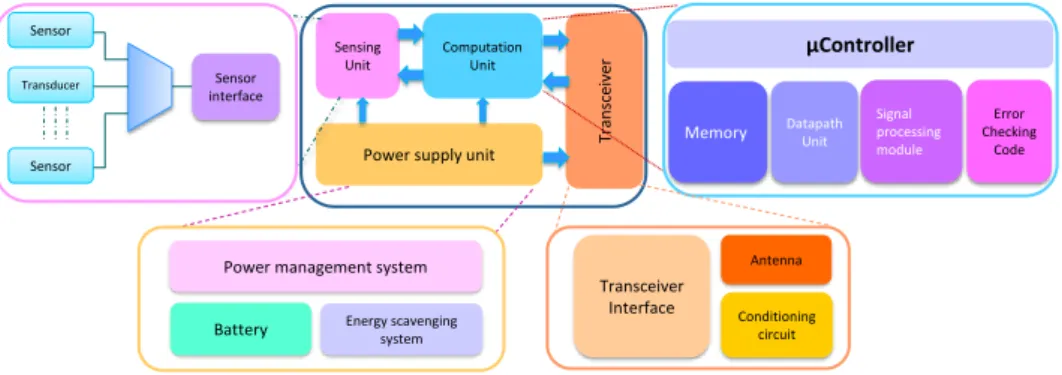
Wireless Sensor Networks (WSN) are networks of distributed sensors used to monitor environmental conditions such as motion and temperature [47][48] and can extend to other measuring and monitoring endeavors. The collected data is then sent through this network until it reaches a sink, where it can be analyzed. A node in a WSN combines sensing,
4
computing and communication tasks, and is usually structured as shown in figure 1.9. The sensor or actuator in the sensing unit can be any type of sensor, and a WSNN can have either one type of sensors or a complex mix of different sensors, depending on the application. Because sensed values are analog, there needs to be an analog-to-digital converter (ADC) or some sort of convertion interface to allow the sensors to communicate with the rest of the circuit. The digital collected data is then sent to the computation
unit, which then analyses and evaluates the data. If the data is to be sent to the sink (a
message), then the transeiver sends it to the nearest neighbor WSNN in the network (or depending on the communication algorithm used), which upon receiving it, transfers it in turn to the next WSNN until it reaches the sink. However, this scenario represents the ideal case. A more frequent and easier to implement scenario is the one where the sink is central node and the wireless sensor network nodes are directly connected to it.
Nevertheless, which ever the scenario, a node in a WSN has two jobs, the first is to monitor the environment, and the second is to transfer the data through the network. Once one of these is finished, the node goes to sleep, and wakes up only at scheduled times to either check if it has to pass along a message, or to collect environmental data. This duty cycling allows the node to be more power efficient, especially in the case of autonomous WSN placed in remote [49] or difficult to access areas [50].
Sensing Unit
Power supply unit
Computation Unit Tr an sc eiver Memory µController Error Checking Code Datapath Unit Signal processing module Antenna Transceiver Interface Conditioning circuit Sensor Sensor interface Transducer Sensor Energy scavenging system Battery
Power management system
Figure 1.9: Typical architecture of a WSNN
1.3.3.2 Variations and energy efficiency in a WSNN
The variations affecting a WSN are variable and depend on the type of WSN or its ap-plication. We can however generalize some of them. The first type of variations are PVT variations, which affect all circuits. Since some of the WSN applications are in remote areas or in harsh environments [50], these variations can have a big impact on the node’s operation.
The second type of variations affecting a WSN are the applications variations. The first level of variations occur when there are different sensors on the same node, each with its own energy needs. An imager may consume a hundred times more than a simple temperature sensor. The node needs to adapt its energy expenditure depending on the type of application. The second level of variation is within the application itself. Taking the example of an imager, we may need to simply detect the presence of something in the place being monitored, or we may need facial recognition as well. The difference in accuracy can have an important impact on the energy as shown in figure 1.10. Moreover, as the demand for more efficient IoT systems grows, there needs to be circuits capable of covering many WSN applications, especially the ones used in the Internet of Things (IoT) at a low cost and capable of handling different energy needs.
Applications
Video surveillance Smart Camera Secure communications
Data Fusion Tracking and Monitoring
Energy needs
pW-μW area mW area
Figure 1.10: Energy needs of IoT application [8]
On top of the variations, energy efficicency in a WSNN is compromised due to the nature of the WSN, and the duty cycling, where the node is woken up and put back to sleep at scheduled intervals (figure 1.11). If there is no information to pass along, then the energy for waking up the node is lost. On the other hand, if data is sent during the sleep time of the node, it cannot be received and is lost. The sink will request this data again, prompting another operation, which is wasteful. The duty cycling has to adapt to the network and be as efficient as possible. The introduction of more efficient communication algorithms for WSN [51][52] as well as the increase of wake up radios [53][54] integration may be a viable solution to this problem.
P(W) t(s) t t actif sleep
Figure 1.11: Duty cycling in a WSN
1.3.4 Conclusion
The variations affecting the circuit described above are becoming increasingly present in complex and modern circuits. Several solutions are proposed to avoid them. One of the most promising method is based on the assumption that by monitoring these variations, we can adapt the circuit to perform at its best instead of working with a rigid set of constraints and margins.
In the following sections, technological and architectural design proposal are presented, focusing mainly on proposals geared towards adaptation, as it not only answers the vari-ations problem, but does it in an energy efficient way.
1.4
Technological solutions to counter variation
Several technological propositions to overcome the problems of variability and energy efficiency were proposed, some at process level while other at device level. At process level, a constant improvement of the processes through modeling [45] and technique enhancement [55], as well as a better understanding of the physics is always occurring. At device levels, several candidates to replace the traditional MOSFET device has been proposed, chief among them the thin film technology on which is based the UTBB FDSOI5 technology
5
and the FINFET6[56].
The FINFET is a 3D structure, of which a first version was persent by Berkeley pro-fessor Chenming Hu and his team [57] in 2000. Its gate is elevated and forms a fin (hence the name) nearly surrounding the device as shown in figure 1.12. In this architecture, the channel is extremely thin and the gate is used to control the leakage. The device can have several gates instead of one, as is the case with Intel and their tri-gate FINFET [58]. Al-though this technology is very promising and has already been used in several chips from Intel[59], GlobalFoundries[60] and AMD[61], it is still not mainstream and faces many challenges.
Another interesting device is the UTBB FDSOI , which thanks to its Back Biasing, can control and change its characteristics, and allow a more adaptive use of the device. In this work, we chose to use the UTBB FDSOI 28nm technology, as it offers the best compromise between power and performance.
Figure 1.12: Layout and cross section of a Finfet device [9]
1.4.1 FDSOI technology for adaptation and targeted applications
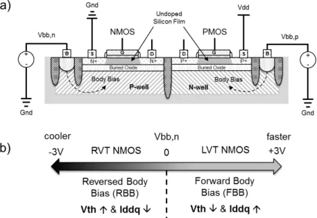
UTBB FDSOI was introduced by LETI and STMicroelectronics as one of the most ad-vanced technological answers to mitigate the effect of variability on a circuit and to achieve better energy efficiency and control over the circuit. This technology provides several op-tions for controlling the speed and the leakage of a device thanks to the Back-Biasing (BB) technique. It offers the possibility of dynamically increasing the speed of the device through Forward Back Biasing (FBB), and as such increase the performances, or using the Reverse Back Biasing (RBB) to decrease the leakage current. In the following section, an overview of the UTBB FDSOI technology is given, most of which were reported in [62], [63] and [8].
1.4.1.1 Introduction to the UTBB FDSOI technology
As its name indicates, the UTBB FDSOI 28nm technology is characterized by a Silicon-insulator-silicon layer instead of the traditional silicon substrate used, as shown in figure 1.13. The inclusion of the Ultra Thin Buried Oxide (BOX) allows for a better control of the channel, as it separates it from the substrate, allowing for a better Drain/Source-to-Substrate parasitic capacitance and body factor. The channel is thus created in a thin dopant-free silicon layer, and with the raising of the drain and source, the access resistances is also reduced.
6
Source e- Drain
Gate
(a)
Source e- Drain
Gate
Ultra-Thin Buried Oxide
(b) (c)
Figure 1.13: (a) CMOS in bulk, (b) UTBB FDSOI MOS device, (c) cross section of a MOS device [10]
In addition, a back plane (n-type for N-wells and p-type for p-well) is also created under the BOX, in order to improve the Short Channel effect and adjust the threshold voltage (Vth). By using the Back Biasing voltage Vbb, which can range from -3V to 3V, the Vth and the leakage current can be adjusted and fine tuned to the application and achieve the best performance/power trade-off, which is not possible when using the bulk technology.
Finally, to electrically isolate the devices, Shallow Trench Isolation (STI) are imple-mented. Figure 1.14 shows a cross-section of a CMOS device as well as the body biasing range.
Figure 1.14: (a) cross section of a CMOS device, (b) body biasing range
In terms of frequency and energy, the UTBB FDSOI proved to be more efficient than
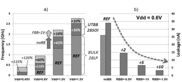
bulk when using either the FBB or RBB. Figure 1.15(a) shows the considerable speed
gain achieved through Forward Back Biasing. Depending on the Vbb used, the gain in frequency can increase by 40%. The same is also achievable when using Reverse Back Biasing, although on the opposite scale, where the leakage current can be decreased by as much as 5 times at a standard standby voltage (Vdd) of 0.6V as shown in figure 1.15(b). Both performance results are extracted from electrical simulations of the critical path of an ARM64.
Figure 1.15: (a) Frequency at different FBB Vbb, (b) Leakage current for different RBB Vbb
during activity periods when necessary, especially when an energy/performance trade-off is necessary to adapt to variations due to applications. In idle mode, back biasing will help decrease leakage power.
1.4.1.2 UTBB FDSOI technology in Near Threshold
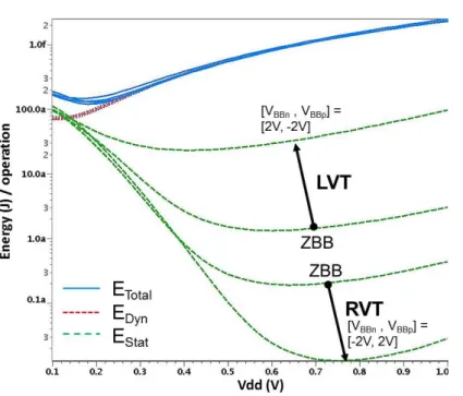
Another interesting characteristic of the FDSOI technology is its low Minimum Energy Point (MEP), which is the operating voltage for which the total energy consumed per operation is minimized. In this case, The MEP is situated in the [0.2V, 0.4V] range for both LVT7 and RVT8 devices, as shown in figure 1.16. The figure also shows us how this
MEP changes when applying Back Biasing. We can observe that although the total energy for both devices is close, the static energy for LVT and RVT is different, and when applying a Back Biasing Voltage, these curves behave differently, where the LVT curves goes up while the RVT curve goes down. The ZBB (Zero Back Biasing) point represents the initial curve in the absence of all back biasing. These results are from electrical simulations of ring oscillators.
7Low Vth 8
Figure 1.16: Minimum Energy point for RVT and LVT FDSOI technologies
Moreover, when comparing leakage and delay of 8bits full adders in different technolo-gies (FDSOI 28nm, FINFET 14nm and bulk 28nm) at different MEPs (figure 1.17), it is clear that the RVT FDSOI technology has the lowest energy levels, even if the delay is considerable compared to the FINFET 14nm technology. The bulk 28nm technology shows the worst results for both the delay and the leakage.
Figure 1.17: Energy and delay at MEP: a technology comparison
1.4.1.3 Poly Biasing in UTBB FDSOI
Another interesting feature of the FDSOI technology is the option for increasing the Poly
Biasingof LVT devices, where the gate length is customized to achieve the best
energy/de-lay compromise. Figure 1.18 shows the MEP for different poly biasing (PB0= no increase, PB4= 4nm gate enlargement, PB16= 16nm gate enlargement) as well as a regular RVT device, as the poly biasing is only applied to LVT devices. We can observe a 15% decrease in energy per operation for the same frequency (500MHz). The PB16 technology is better energy-wise than the RVT.
It is however difficult to integrate both RVT and LVT due to the wells isolation. A co-integration of different poly biasing LVT devices is however possible, and most interesting for IoT and sensor nodes applications. Although RVT is better in case long periods of sleep mode are expected, as RVT reduces the leakage.
Figure 1.18: Energy at MEP for different poly biasing options and RVT
1.4.1.4 Conclusion
UTBB FDSOI 28nm technology represents a good fit for IoT applications and offers a good performance/energy consumption trade off. It has a low variability, is compatible with Ultra Low Voltage (ULV) and Ultra Wide Range Voltage (UWVR), with a low cost production. The possibility of back biasing and poly biasing offer the possibility of adapting the circuit performances as well as its energy expenditure.
1.5
Architectural solutions for performance and energy
ef-ficiency
While the technological innovations to deal with the variations affecting a circuit help resolve the problem of the leakage power, which is predominant in advanced nodes, it needs to be coupled with architectural solutions, that can also address the environmental variations as well as regulate the dynamic power consumption. As mentioned in section 1.2, there are several parameters that can be changed to reduce the power consumption, or deal with the variations.
1.5.1 Voltage supply and frequency adjustments
One obvious way to decrease the power consumption in any circuit but especially in WSN nodes is to duty cycle it, where the node wakes up when requested and processes the data, and upon finishing, goes back to a sleeping mode. During the sleep mode or idle mode, the circuit blocks are disconnected and no longer consume power.
There are several ways to implement an idle mode, depending on the application and the hardware available. The first one is done by clock gating, where the clock of a block or a frequency domain is disabled, which then stops the sequential elements from switching, and thus eliminate the internal activity α, suppressing any dynamic power. Once clock
power gate any block in order to remove the leakage power. Power gating is done by
locally turning off the supply voltage of any block, and reducing the leakage power to almost zero, with the exception of the transistor used for power gating. Figure 1.19 shows how clock gating and power gating can be implemented.
VDD OUT Clk IN GND HW EN (a) VDD OUT Clk IN GND EN HW (b)
Figure 1.19: (a) Clock gating of a block, (b) Power gating of a block
Instead of completely turning off the frequency or the supply voltage, it is possible to change the performances of the circuit by dynamically changing its frequency and voltage through DVFS9 as shown in figure 1.20.
Figure 1.20: DVFS implementation [11]
DVFS is a commonly used technique for power reduction, where the frequency of a block is decreased, to allow for a voltage reduction following the PDynamic = CF V2 law, with α the switching activity. There are several algorithms and methods to detect which frequency/voltage couple is best are used, however, they can be being quite expensive hardware and even energy-wise. Moreover, a strict DVFS is not easy to implement, as the voltage regulators are notoriously difficult and expensive to implement, especially the DC/DC blocks.
Two techniques can be implemented to resolve this problem: Vdd-hopping or Vdd-dithering.
Vdd-hopping is a strategy where the supply voltage is stabilized at a certain point and remains constant for a certain frequency fclk range. Once the frequency is decided, the corresponding supply voltage is applied, and changes as the frequency changes as shown in figure 1.21.a. The problem in this case is that the frequency/voltage couple is not optimal as the fclk moves from the left edge towards the right. To compensate for that, Vdd -dithering can be used instead of Vdd-hopping. Instead of sticking to one voltage value over a certain fclk range, the supply voltage is stabilized at an optimal point of the interval, depending on the switching ratio, which corresponds to the time spent at low Vdd and
9
high Vddas shown in figure 1.21.b. This allows the implemented scheme to follow the ideal DVFS curve.
Figure 1.21: Voltage-frequency for DVFS strategies. (a) Vdd-hopping, (b) Vdd-dithering [12]
One step above DVFS is AVFS10, which is similar to DVFS, but can adapt to to
variations. While in DVFS the voltage/frequency point is pre-determined depending on the application, AVFS eliminates margins entirely, it adapts to the variations, and changes the frequency/voltage couple accordingly at runtime.
Ultimately, the choice between which power reduction technique to use depends on the application and the power budget. Clock gating is a simple logical operation, that doesn’t need any set up time, while power gating operation necessitate an additional amount time when turn on and off, introducing more latency into the circuit and power loss. When powering down, it is necessary to back up the values in the registers and the data in the memory, and when powering up, a set up time to reestablish the correct voltage level is needed. DVFS and AVFS on the other hand demands important additional circuitry and can be quite hard to implement. In this regard, it is the application, the reaction time wanted and the grain(fine-grain or coarse-grain) of the hardware that determines which technique to use. In a majority of circuit, a fine-grain power domain is used, allowing small blocks to be turned on and off when needed.
Another DVFS technique used to adapt the performances of the circuit that doesn’t require additional circuitry, is to adapt the supply voltage value to the application, by choosing in which working range to supply the circuit. As the transistor has three main working ranges: the nominal, the ULV and the NTC11, we can chose in which range to
supply it in order to obtain the best energy efficiency possible. To reduce the power consumption, is it possible to supply the circuit at its MEP12 in the ULV13 range of the
transistor as shown in figure 1.22. The MEP is obtained when the sum of the dynamic and static energy is at a minimum. The MEP also acts as an energy indicator, when the energy is below this point, the static energy is more important than the dynamic energy and vice-versa. As shown in figure 1.22, the frequency at the MEP voltage VM EP can be divided by 25. When supplying the circuit at NTC, the frequency is only divided by 5 and the energy by 4. So by wisely choosing in which range to supply the circuit, it is possible to change it performances significantly.
However, to supply the circuit below the nominal level opens the door to other prob-lems. The more the supply voltage is reduced, the more the Ioncurrent will be sensitive to
10Adaptive Voltage and Frequency Scaling 11
Near Threshold Computing
12Minimum Energy Point 13
the variations of the threshold voltage ∆VT H, which will need to be countered by increas-ing the gate area, as the ∆VT H is inversely proportional to the square of the gate area. Timing problems also abound when the supply voltage is lowered, since the flip-flops and
latches no longer have a proper hold time, and the clock skew is increased. Moreover, in
order to implement multiple power domains, it is necessary to use level shifters, and these are notoriously affected by all PVT variations.
It is however worth noting that these problems only affect synchronous circuit, while asynchronous circuit are robust towards supply voltage variations, which makes it a good candidate for ULV and NTC applications.
Figure 1.22: Energy and performance as a function of the supply voltage in the ULC, NTC and nominal operation range [13]
1.5.2 Architectural solutions for energy efficiency
1.5.2.1 Digital solutions and functions
Other than changing the supply voltage and the circuit frequency, it is possible to play on the architecture of the circuit itself, or the software running on top in order to lower the power and energy consumption.
There are several techniques used to achieve this effect. The first one is to simply dedi-cate different hardware to different application as shown in figure 1.23 and as is the case in the TI CC2650 system, where a Low Power (LP) and High Power (HP) processor coexist. The LP processor deals with the common tasks, while the HP processor is only used when complex computing is needed or for unexpected tasks. In this case, the HP processor can remain on an idle mode until awakened, while the LP processor deals with the mundane tasks and can also be switched to an idle mode, or can awaken the HP processor. While the HP processor is not energy efficient, this partitioning allows for more flexibility and to adapt to different applications while still achieving a maximum of energy efficiency.
LP
Processor
HP
Processor
LP
memory
HP memory
Figure 1.23: Multiprocessor system with a low power (LP) dedicated memory and processor, and a high power (HP) processor and associated memory
It is also possible to use hardware accelerators and dedicated instructions to deport parts of the code that is routinely executed by dedicated hardware via an external mod-ule, such as AES14, CRC15 or an RNG16 as is the case of the STM32L0 [64] or via
dedi-cated DSP instructions like the MAC17or the SIMD18, used extensively for filtering or in
FFT19. These solutions considerably improve the energy efficiency of the system and are
even developed today in general processors like the ARM Cortex-M4 with the ARMV7-M instruction set [65].
It is possible to use other techniques such as load balancing, task mapping or even adequate computing to achieve better energy efficiency. The choice rests solely on the applications targeted and the cost, as these techniques can be quite costly.
1.5.2.2 Analog and radio-frequency functions
Another reason to try to achieve energy efficiency through other methods rather than de-creasing the supply voltage is analog blocks, as they respond poorly to decreased supply voltage. This is especially important as sensor nodes incorporate RF circuitry, which can consumes up to 70% of the node’s power [66], especially in recievers where the frequency synthesis and the amplification path consume more than 60% of the total power consump-tion [67]. A first alternative is to implement a wake-up radio, which is a secondary radio capable of monitoring the channel and instruct the main radio to turn off when there is no activity detected. The goal would be to first eliminate the power lost due to the tran-siever idle listening, and then to minimize the energy expenditure for the common tasks. Extensive duty cycling can be used to resolve the first problem, however, it can lead to the loss of data when in sleep mode. Other methods proposed range from zero margin implementation, self-healing [68] or adaptive radio [69][70]. The problem in most cases is that the performance degradation is not worth the energy saving, as is the case with the ATMEL AT86RF233 which can tune its sensitivity by 50%, but only achieves a 20% in power reduction [71].
14Advanced Encryption Standard 15
Cyclic Redundancy Check
16Random Number Generator 17
Multiply-Accumulate
18Single Instruction Multiple Data 19
In the case of imagers for example, the way to reduce the power consumption comes through the compression and decrease in the transferred data. By only selecting and sending relevant data based on the sensor’s criteria, it is possible to reduce the power consumption of the circuit. Another method for power reduction is to play on the signal quality [72][73]. These methods are however costly and more complex to implement.
The methods used to reduce power in analog blocks are as diverse as the analog blocks themselves, as one solution that works for one analog circuit will not work for a hundred others, and as such, the research is still continuing.
1.5.3 Block’s adaptation for energy efficiency
Another way of viewing things is to react to the application, the environment or the energy budget instead of making them the constraints. In a typical circuit, and in order to enforce a strict QoS20, margins are put in place to respond to the worst case scenario.
However, these margins cause significant power and energy efficiency loss, as the circuit is not always, if ever, confronted to the worst case scenario. The ideal would be to have a system that can react according depending on the scenario. When on a best case scenario, the circuit would be able to adjust its performances in order to spend the less power possible, while an increase in power consumption would be seen as necessary in case of a worst case scenario. By eliminating these margins, it is possible to achieve the best performance/power consumption trade-off. There are several techniques to do that. 1.5.3.1 Dynamic adaptation
Concerning the dynamic adaptation techniques used in almost all the circuits discussed below, two main ones are predominant: the automatic control which is well known and used in the majority of circuit, and the newly expanded field of machine learning. In the first case, the circuit operates under certain assumptions and for certain values. When these values change, the circuit performances evolve to adapt to the new parameters. Depending on the parameters, their changes and the feedback loops used, the circuit already knows how to react, and only reacts when these parameters change. In the case of machine learning however, the circuit’s tasks and responses are not pre-programmed, and the circuit is expected to learn to adapt to the application and environment, which needs complex dedicated computing infrastructures and time to learn.
While the first technique is widely used and recognized, it is not always energy effective, as it allows for certain margins. In the case of machine learning, as it learns, it adapts more quickly and efficiently, however, it may need too many resources before achieving significant results. In most blocks, control loops are integrated to achieve the necessary adaptativity.
1.5.3.2 Monitoring
The first and most used technique for adaptation is circuit monitoring. Monitoring can have many purposes, from thermal monitoring [74] in order not to damage the circuit, to fault monitoring [75] and PVT monitoring[76] to compensate for errors in the circuit and to adjust the circuit parameters when affected by PVT variations. Monitoring the circuit’s parameters allows the circuit to not only correct the issues at hand, but also to adjust its performances and respond to the workload accordingly. When using thermal monitors in
20
![Figure 2: Technical Constraints facing IoT [2]](https://thumb-eu.123doks.com/thumbv2/123doknet/12709500.355973/14.893.154.785.128.667/figure-technical-constraints-facing-iot.webp)
![Figure 1.1: Path delay standard deviation to mean ratio for D2D and WID variations versus path type for different gates [3]](https://thumb-eu.123doks.com/thumbv2/123doknet/12709500.355973/21.893.247.688.156.442/figure-path-delay-standard-deviation-variations-versus-different.webp)
![Figure 1.4: Logic path delay as a function of the supply voltage [6]](https://thumb-eu.123doks.com/thumbv2/123doknet/12709500.355973/23.893.319.610.341.562/figure-logic-path-delay-function-supply-voltage.webp)
![Figure 1.5: Influence of the temperature on the characteristics of a transistor and on path delay [6]](https://thumb-eu.123doks.com/thumbv2/123doknet/12709500.355973/24.893.193.745.135.325/figure-influence-temperature-characteristics-transistor-path-delay.webp)

![Figure 1.22: Energy and performance as a function of the supply voltage in the ULC, NTC and nominal operation range [13]](https://thumb-eu.123doks.com/thumbv2/123doknet/12709500.355973/35.893.164.772.391.654/figure-energy-performance-function-supply-voltage-nominal-operation.webp)
