HAL Id: hal-03017538
https://hal.archives-ouvertes.fr/hal-03017538
Submitted on 20 Nov 2020HAL is a multi-disciplinary open access archive for the deposit and dissemination of sci-entific research documents, whether they are pub-lished or not. The documents may come from teaching and research institutions in France or abroad, or from public or private research centers.
L’archive ouverte pluridisciplinaire HAL, est destinée au dépôt et à la diffusion de documents scientifiques de niveau recherche, publiés ou non, émanant des établissements d’enseignement et de recherche français ou étrangers, des laboratoires publics ou privés.
Molecular Functionalization of Chemically Active
Defects in WSe2 for Enhanced Opto-Electronics
Yuda Zhao, Sai Manoj Gali, Can Wang, Anton Pershin, Amine Slassi, David
Beljonne, Paolo Samori
To cite this version:
Yuda Zhao, Sai Manoj Gali, Can Wang, Anton Pershin, Amine Slassi, et al.. Molecular Functional-ization of Chemically Active Defects in WSe2 for Enhanced Opto-Electronics. Advanced Functional Materials, Wiley, 2020, 30 (45), pp.2005045. �10.1002/adfm.202005045�. �hal-03017538�
1
Molecular Functionalization of Chemically Active Defects in WSe2 for Enhanced
Opto-electronics
Yuda Zhao, Sai Manoj Gali, Can Wang, Anton Pershin, Amine Slassi,David Beljonne, Paolo Samorì*
Dr. Y. Zhao, Dr. C. Wang, Prof. P. Samorì
University of Strasbourg, CNRS, ISIS UMR 7006, 8 allée Gaspard Monge, F-67000 Strasbourg, France
E-mail: [email protected]
Dr. S. M. Gali, Dr. A. Pershin,[+]
Dr. A. Slassi, Prof. D. Beljonne
Laboratory for Chemistry of Novel Materials, University of Mons, 7000-Mons, Belgium
[+]Presnet address: Wigner Research Centre for Physics, PO Box 49, H-1525 Budapest,
Hungary
Keywords: transition metal dichalcogenides, vacancy defect, thiol chemistry, field-effect transistor, photoluminescence
Structural defects are known to worsen electrical and optical properties of two-dimensional (2D) materials. Transition metal dichalcogenides (TMDs) are prone to chalcogen vacancies and molecular functionalization of these vacancies offers a powerful strategy to engineer the crystal structure by healing such defects. This molecular approach can effectively improve physical properties of 2D materials and optimize the performance of 2D electronic devices. While this strategy has been successfully exploited to heal vacancies in sulfides, its viability on selenides based TMDs has not yet been proven. Here, by using thiophenol molecules to functionalize monolayer WSe2 surface containing Se vacancies, we demonstrate that the defect healing via
molecular approach not only improves the performance of WSe2 transistors (>10-fold increase
in the current density, the electron mobility, and the Ion/Ioff ratio), but also enhances the
photoluminescence properties of monolayer WSe2 flakes (three-fold increase of PL intensity at
room temperature). Theoretical calculations elucidate the mechanism of molecular passivation, which originates from the strong interaction between thiol functional group at Se vacancy sites and neighboring tungsten atoms. These results demonstrate that our molecular approach
2
represents a powerful strategy to engineer WSe2 FETs and optimize their optical properties,
paving the way towards high-performance 2D (opto)electronic devices.
1. Introduction
Atomically thick two-dimensional materials display numerous outstanding physical and chemical properties. In particular, their high immunity to short-channel effects have shown promising applications in next-generation field-effect transistors (FETs).[1-3] The star 2D
semiconductor, i.e. MoS2, exhibits high electron mobility ranging from 10 to >100 cm2V-1s-1 at
room temperature and large Ion/Ioff current ratio (>105),[4-6] thereby outperforming Si transistors
with similar channel thickness.[7] Compared with the extensively studied MoS
2 devices, the
transport behavior of monolayer WSe2 FETs shows stronger dependence on the contact metal
and the surrounding dielectric environment, exhibiting different transport modes (unipolar/ambipolar) and varying dominant carriers (electron/hole).[8-10] In addition, large
discrepancies of carrier mobility in 2D transistors between theoretical predictions and experimental results can be found in literature.[11-14] These all inspire researchers to study the
impact of intrinsic and extrinsic defects in 2D materials on their charge transport properties in transistors.[15]
The main type of intrinsic defects in monolayer MoS2 prepared by mechanical exfoliation
method using scotch tape and chemical vapor deposition (CVD) method has been identified as sulfur vacancies.[16-18] The concentration of single sulfur vacancy has been estimated at over 1
× 1013 cm-2 in monolayer mechanical exfoliated samples.[19] This number can reach 8.6× 10¹³
cm-2 in monolayer CVD samples, which corresponds to 3% of S content in MoS2.[20] These
vacancies induce localized defect states and result in the hopping transport of charge carriers in 2D layers.[21]
The molecular approach has been widely exploited to functionalize 2D materials.[22, 23] The
3
performance with band-like transport behavior and the electron mobility as high as 150 cm2V -1s-1.[24-26] On the same time, the passivation of defects can dramatically improve the optical
properties of 2D layers, for example reaching photoluminescence quantum yields in MoS2
approaching the unity.[27] Therefore, it is of vital importance to study the intrinsic defects in
WSe2, analyze the correlation between the defects and the physical properties of WSe2, and
finally explore the molecular methods to passivate the defects in order to improve optical properties and device performance.
In our work, thiophenol molecules are functionalized on intrinsic Se vacancies of WSe2 samples,
which has been directly identified by scanning tunneling microscope (STM) imaging for the first time. The improved charge transport in monolayer WSe2 back-gate FETs and the efficient
photoluminescence (PL) emission of monolayer flake after thiophenol functionalization experimentally demonstrate the successful defect passivation via the molecular approach. WSe2
FET show an over 10-fold increase in the current density, the electron mobility, and the Ion/Ioff
ratio. Theoretical calculations indicate that a strong interaction of thiol functional group with Se vacancies in WSe2 determines the elimination of defect states and the shift of work function
via n-type doping effect. Our combined experimental and theoretical research represents a viable route to engineer defects in the monolayer WSe2 towards high-performance transistors
and high-efficiency photoluminescence materials.
2. Results and Discussion
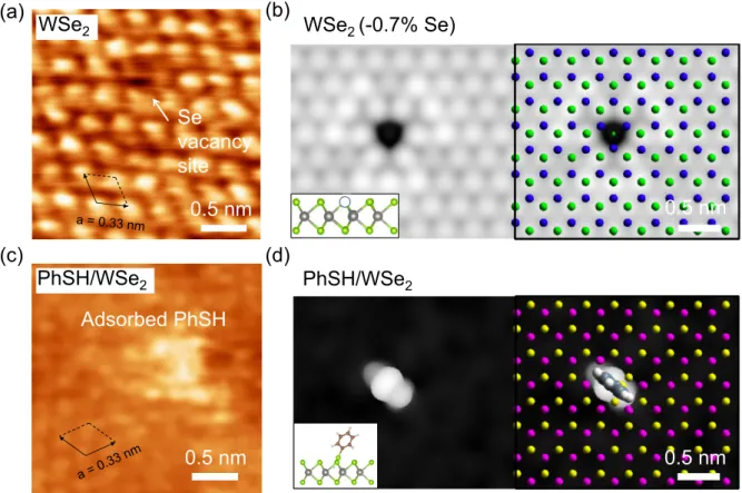
Intrinsic defects in WSe2 are firstly identified by STM imaging in ambient conditions on a
freshly mechanically exfoliated surface of WSe2 crystals. Figure 1a and Figure S1 show the
atomic resolution STM height image of WSe2. It displays a lattice constant of a = b = 0.33 nm
and γ=120°, in good accordance with theoretical lattice parameters. Some point-like defects (dark circular feature in the STM image) are observed in the two-dimensional Se atom arrays. Theoretical calculations reveal that from an energetic viewpoint, the energy required to form
4
Se vacancies, exposed in the outer surface, is lower compared to the generation of vacancies of W, which are embedded in the underlying layer. [28, 29] We infer that the defects observed in the
STM image are most likely Se vacancies, and the simulated STM image showing the surface electron state of WSe2 with 0.7% Se vacancy in Figure 1b further confirms our interpretation.
The strong brightness difference between W and Se atoms indicate the electron rich nature in the Se sites on the crystal surface, and the missing of one bright dot refers to a Se vacancy site. Molecules with hydroxyl, thiol or selenol functional groups are promising candidates to passivate Se vacancies in monolayer WSe2. Considering of the steric effect in Se vacancy sites,
molecules with thiol or selenol functional group are more suitable for passivating single-point Se vacancies. Compared with thiolated molecules, selenol molecules can be easily oxidized and their thermal stability is quite poor,[30] as also demonstrated by our device characterizations in
the latter sections. Therefore, in this work we mainly focus our attention on the use of thiolated molecules, i.e. thiophenol (abbreviated to PhSH in the figures) to repair Se vacancies on WSe2
surface. We implemented a vapor-phase deposition method to exclude the contribution from solvents in the common solution processing.[31] Specifically, the thiophenol molecules are
heated in a sealed bottle with WSe2 samples directly exposed to the molecular vapors. After the
molecular adsorption, the WSe2 surface was immediately covered with a drop of 1-phenyoctane
and characterized by STM at the liquid/solid interface. The high-resolution image in Figure 1c shows a bright dot, which can be ascribed to an adsorbed thiophenol molecule filling the Se vacancy. The weakly bonded physisorbed thiophenol molecules have been dissolved in 1-phenyoctane, thus has desorbed from the WSe2. Hence, they cannot be visualized under our
scanning condition. The adsorption configuration of a thiophenol molecule on the single Se vacancy site was confirmed by the comparison between theoretical simulations and experimental STM images. Two possible adsorption configurations are selected including the vertical (benzene ring arranged perpendicular to the 2D basal plane, Figure S2a) and horizontal (benzene ring lying flat and parallel to the 2D basal plane, Figure S2b) packing of thiophenol
5
on WSe2 surface. By comparing the calculated adsorption energy at the two configurations
(vertical: −0.83 eV and horizontal: −0.60 eV), we conclude that thiophenol molecules are prone to adsorb vertically at the Se vacancy site. The simulated STM images of the adsorbed thiophenol molecule at the vertical stacking configuration (Figure 1d) is consistent with the experimental STM images (Figure 1c). By gradually decreasing the tip-sample distance, the STM tip could reach the position under the phenyl group of thiophenol. As seen in Figure S3, the underneath Se atom arrays become clear with no point defect, while the bright dots referred to thiophenol are still observable. This set of STM images can also demonstrate the vertical stacking configuration of thiophenol on WSe2 surface. Meanwhile, these vertically adsorbed
molecules are quite stably attached to the Se vacancy points.
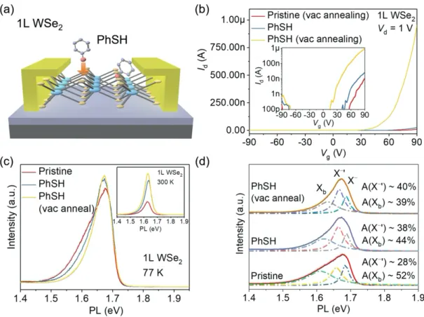
After the successful demonstration of thiophenol functionalization on Se vacancy sites in WSe2
by the STM characterization, it is very important to explore the effect of defect passivation on the material properties and the FET performance. The scheme of the FET device architectures is portrayed in Figure 2a. A back-gate monolayer WSe2 FET was fabricated on the SiO2/Si
substrate with Au metal electrodes. After device fabrication, a vacuum annealing process was performed in order to remove the surface contamination and expose the vacancy sites. Then thiophenol molecules were functionalized on the monolayer WSe2 surface to passivate Se
vacancies. The effect induced by molecules on the transfer characteristics of WSe2 FET is
displayed in Figure 2b. The molecular functionalization increases the on-current level, improves the field-effect mobility (from 0.015 to 0.025 cm2V-1s-1), and enhances the I
on/Ioff ratio
(from 1 × 10⁴ to 3 × 10⁴). In order to increase the density of strongly grafted molecules, a second
vacuum annealing process was conducted to enhance the interaction between molecules and vacancy sites. Compared with the pristine WSe2 devices, the annealing process induces the
increase of the drain current at Vg = 90 V by almost two orders of magnitude, the improvement
of electron mobility from 0.015 to 0.79 cm2V-1s-1, and the enhancement of the I
on/Ioff ratio from
6
increase of electron density by 1.04 × 1012 cm-2, exhibiting the n-type doping induced by the
thiophenol molecules. The output curves (Figure S4a) of pristine WSe2 FET show a superlinear
relationship within 1.5 V drain biases, demonstrating a relatively large contact resistance. The molecular functionalization results in a less superlinear output curves (Figure S4b) due to the increased electron density and the decreased contact resistance. Atomic force microscopy (AFM) imaging (Figure S5) was used to monitor the morphology change of WSe2 surface
before and after the second annealing process, providing unambiguous evidence for the removal of weakly physisorbed molecules. Therefore, the strongly adsorbed thiophenol molecules on the Se vacancy sites induce n-type doping on the channel region and greatly improve the FET performance.
The optical property of monolayer WSe2, i.e. PL spectrum, is known to be very sensitive to the
defect states.[32, 33] Therefore, we further studied the effect of thiophenol functionalization on
PL spectra. The room-temperature PL spectra of monolayer WSe2 (inset of Figure 2c) displays
a broad peak centered at 1.63 eV; the chemical functionalization with thiophenol molecules increases the PL intensity of WSe2 by a factor of 2.6. As the temperature decreases,
electron-phonon scattering becomes weak and PL peaks from localized exciton emissions can be more pronounced. The broad PL peak at 77 K (Figure 2c) can be fitted into three peaks in Figure 2d, including one defect-related peak (Xb at 1.61 eV) and two negatively charged trion peaks (X−
at 1.68 eV and X−' at 1.66 eV).[33] The Xb peak originates from the excitons bound to defects,
which can act as an indicator for defects in WSe2.[15] The negatively charged trion peaks are
attributed to the emission from a localized excitation which consists of three charged particles (two electrons and one hole). The thiophenol molecules and the subsequent annealing process together decrease the spectral weight of Xb peak and increase the spectral weight of X−' peak,
demonstrating the successful defect passivation and n-type doping effect.
X-ray photoelectron spectroscopy (XPS) was used to further verify the doping effect from molecules. Figure S6 compares the binding energies for the W 4f5/2, W 4f7/2, Se 3d3/2, and Se
7
3d5/2 peaks before and after molecular functionalization. The binding energies of two W 4f
peaks and two Se 3d peaks are shifted upward by 0.4 eV and 0.5 eV, respectively. It indicates a shift of the Fermi level towards the conduction band. Therefore, XPS characterizations confirm the n-type doping on WSe2 by thiophenol molecules, which is consistent with PL
results.
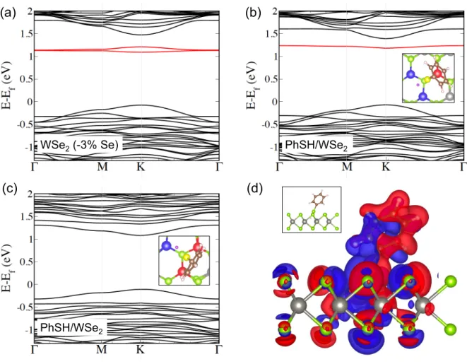
Theoretical calculations were used to study the defect passivation mechanism. Figure 3a shows the electronic band structure of monolayer WSe2 (4 × 4 supercell) with single Se vacancy (3%
Se vacancy concentration, hitherto referred to as WSe2 (–3% Se)) calculated using density
functional theory (DFT). The Se vacancies introduce midgap defect states below the intrinsic conduction band minimum (CBM) at K point by 0.13 eV and 0.18 eV. These relatively deep defect-related localized states should act as traps and limit the electronic charge transport, while simultaneously creating new defect-related optical emission peaks. It explains the inferior performance of FET based on as-prepared WSe2, with low current density and low electron
density (Figure 2b). Furthermore, the defect-related PL peak Xb (Figure 2d) has been observed
at 1.61 eV, which is 0.12 eV smaller than the exciton PL peak X0 at 1.73 eV,[33] in very good
agreement with theoretical prediction of the energy levels of midgap defect states.
The calculated electronic band structure of monolayer WSe2 with thiophenol passivation shows
two possible configurations, as presented in Figure 3b and 3c. While the midgap defect states originating from the Se vacancy were partially recovered in Figure 3b, they are completely recovered in Figure 3c. The atomic configurations pertaining to Figure 3b and 3c were extracted at different time steps along ab initio molecular dynamics (ab-MD) simulations (Figure S7) and differ in the relative positioning of thiol group with respect to the three neighboring tungsten atoms in the vicinity of Se vacancy. As indicated in the inset of Figure 3c, if the sulfur (hydrogen) atom is close to two (one) of the three neighboring tungsten atoms (by ≤ 2.7 Å), a complete recovery of the localized midgap defect states is observed. However, if the sulfur (hydrogen) atom is close to one (two) of the neighboring tungsten atoms, as indicated in the
8
inset of Figure 3b, only a partial recovery of the midgap defect states is observed. This interaction strength between the thiol group and the neighboring tungsten atoms at the Se vacancy site, is further quantified by DDEC6 calculations with specific analysis on bond orders and overlap populations (see Table S1 for details). A non-zero bond order exists between thiol group with neighboring W atoms, which is also responsible for the stability of thiophenol molecule vertically stacked atop Se vacancy. For the atomic and electronic configuration pertaining to Figure 3c (full recovery of midgap defect states), the bond order (overlap population) of sulfur atom with two neighboring tungsten atoms (highlighted in red color in the inset of Figure 3c) is ≥ 0.55 (≥ 0.42), whereas that of hydrogen atom with the remaining tungsten atom (highlighted in blue color in the inset of Figure 3c) is ≈ 0.7 (≈ 0.5). On the other hand, for the atomic and electronic configurations in Figure 3b, the bond order (overlap population) of sulfur atom with two neighboring tungsten atoms (highlighted in blue color in the inset of Figure 3b) is ≤ 0.11 (≈ 0.1), whereas that of hydrogen atom with the same two tungsten atoms is ≥ 0.46 ( ≥ 0.35). For all configurations, the sulfur atom is always connected to the carbon atom (S-C) of the molecule, with a strong covalent character (bond order ≥ 1.0). The main message that ensues from this analysis is that the healing of the midgap electronic states is a dynamic effect, with switching back and forth between configurations like those in Figures 3b and 3c taking place over picosecond timescales. Therefore, it follows that an electron trapped at a given time might be released shortly after when thiolated molecules adopt a more favorable configuration in the vicinity of the Se vacancy. In addition, the calculated work function of pristine and functionalized WSe2 (𝐸!"# in Table S2) is 4.31 eV and 4.10 eV,
respectively. The shift in work function by 0.21 eV, which mostly originates from the axial dipole component of thiophenol molecules, is thus consistent with n-type doping by the molecules. The charge density difference plot of WSe2 with thiophenol in Figure 3d, calculated
as the difference between the total charge density of thiophenol adsorbed on WSe2 (–3% Se)
9
shows a very strong interaction between the WSe2 (–3% Se) surface with thiophenol at the Se
vacancy site.
In contrast, our theoretical calculations (Table S2) show that the stacking of thiophenol molecules on the vacancy-free WSe2 surface and on oxygen passivated Se vacancy can hardly
change the work function of WSe2 layer. Therefore, it is desirable to find a remote control, such
as an external stimulus, to increase the reactivity of the WSe2. This defect engineering process
can be instrumental towards an improved functionalization of the WSe2 layer with thiophenol
molecules to modulate the carrier density of WSe2. We explore the use of a mild etching strategy,
i.e. laser irradiation, to expose and create more vacancy sites. A focused laser beam with a relatively high power density 2.6 × 10⁵ W/cm2 enables to raise the local temperature, promoting
the desorption of molecules physisorbed on the WSe2 surface and even surpasses the
decomposition temperature of WSe2.[34] After 6 min laser irradiation, the transfer curves in
Figure 4a show that the drain current of WSe2 FET at Vg = 80 V decreased by a factor of 4. The
thiophenol functionalization and the following annealing process recovered the drain current and even exceeded the pristine value. Compared with pristine FET device, the drain current, the electron mobility, and the Ion/Ioff ratio increased by a factor of 10. The transfer curves with
different Vg sweep directions in Figure 4b display the change of hysteresis before and after
molecular functionalization. Compared with pristine devices, the hysteresis in the thiophenol passivated devices at Id = 1 nA decreases from 11 V to 7 V, evidencing the reduction of charge
traps associated with vacancies in the WSe2 sheets. Therefore, the improved transistor
performance after thiophenol functionalization including the increased electron mobility and current density can be attributed to the elimination of trap states originated from Se vacancies and the n-type doping effect on WSe2 channel. Control experiments were carried out after laser
irradiation without molecular functionalization. It revealed that the laser irradiation generated more defects and decreased the drain current in the transfer curves. The following annealing
10
process did not recover the drain current (Figure S8), which shows the main function of thiophenol molecules in the defect passivation.
Figures 4c and 4d display the evolution of PL spectra at 77 K after laser irradiation and molecular functionalization. After 1 min laser irradiation, the defect-related peak Xb became
broader and its spectra weight increased from 47% to 61%. After 6 min laser irradiation, another defect-related peak Xb' emerged and the spectra weight of defect-related peaks (Xb and Xb')
further increased to 84%. After the thiophenol functionalization, the defect-related peaks have been greatly suppressed and the intensity of the PL peak originating from trion and exciton emissions increased by a factor of 10. The PL spectra at 300 K (inset of Figure 4c) also show a dramatic intensity enhancement after thiophenol adsorption. From the PL results, we confirm that laser irradiation can induce the desorption of absorbed molecules and the exposure/creation of chemically active defects in WSe2. Moreover, the thiophenol molecules can effectively
passivate the defects, including the intrinsic defects and the created ones. Compared with PL spectra results in Figure 2d, the additional laser irradiation process contributes to a full passivation of defect-related peaks. The "ambient" molecules, i.e. oxygen and water molecules, can be adsorbed on the intrinsic vacancy sites in WSe2, inhibiting the exposure of chemically
active vacancies to thiophenol molecules (Figure S9). The additional laser irradiation process can effectively desorb these adsorbents and promote the interaction of thiophenols with the vacancies.
We extended our study to the use of benzeneselenol molecules to passivate the defect in WSe2
(Figure S10). After molecular functionalization, the drain current at Vg = 80 V dramatically
increased from 8 nA to 276 nA. However, after the vacuum annealing, the drain current at Vg
= 80 V decreased to 62 nA. Compared with thiophenol passivation, benzeneselenol molecules induce a stronger n-type doping effect on WSe2, which is consistent with our theoretical
calculation results (Table S2). However, the thermal stability of benzeneselenol is much worse than that of thiophenol.[30] The decomposition and the desorption of benzeneselenol molecules
11
greatly affected the interaction of molecules with Se vacancy sites. Therefore, we can conclude that thiolated molecules are more suitable to passivate defects and modulate the carrier density in WSe2. Further studies (for example the exploration of molecular deposition conditions) can
be conducted to enhance the selenol/vacancy interaction to enrich the molecular functionalization strategy on transition metal diselenides.
We further test the stability of thiophenol-passivated WSe2 FET. The transfer curves in the
thiophenol-passivated device displayed good drain current stability during the three days of storage in the glovebox (Figure S11). In comparison, the drain current in the transfer curves of the pristine device degraded after three days of storage. This is because the chemically active vacancy sites in the pristine device can be unintentionally doped by gas molecules in the surrounding environment. Therefore, thiophenol can effectively passivate the vacancy defects in WSe2 and improve both the material stability and the device performance.
3. Conclusion
In summary, we have imaged by STM the intrinsic Se vacancies on the freshly exfoliated WSe2
samples and showed the adsorption of thiophenol molecules at the chemically active Se vacancy sites for the first time. By studying the carrier transport in monolayer WSe2 back-gate FETs and
PL spectra of monolayer flake we demonstrated that thiophenol molecules are capable to passivate the defect states in WSe2. The passivated monolayer WSe2 FETs exhibit higher
current density (an increase of Id at Vg = 90 V by a factor of 100), improved electron mobility
(from 0.015 to 0.79 cm2V-1s-1) and increased I
on/Ioff ratio (from 1 × 10⁴ to 1 × 10⁶). A decrease
in defect-related PL peak intensity also indicates the effective passivation of defects in monolayer WSe2. Theoretical calculation provided unambiguous evidence for the formation of
strong interaction between the thiol group of the molecules and Se vacancies in WSe2 yielding
n-type doping and the dynamic recovery of defect states originating from Se vacancies. Furthermore, the defect engineering in WSe2 by laser irradiation enables to create more
12
chemically active defects, which can be effectively passivated by thiophenol molecules. Our molecular approach to engineer defects in WSe2 flakes is a powerful strategy that can be
extended to other transition metal diselenides, enabling functional diversity for high-performance TMD-based electronic devices
4. Experimental Section
Materials: Bulk WSe2 crystals were purchased from commercial vendors (HQ graphene). The
thiophenol (Product No. 240249) and benzeneselenol (Product No. 375152) were purchased from Sigma-Aldrich.
Molecular functionalization on WSe2: The substrates holding WSe2 FETs or monolayer flakes
were fixed onto the lid of a 20 mL glass container filled with 100 μL of thiophenol. The lid was closed with the sample surface facing the liquid, and the container was saturated with molecular vapor by heating at 50 oC for 15 min. All the process was carried out under inert atmosphere
(N2-filled glovebox). Solvent molecules, especially oxygen-containing molecules (such as
ethanol), have the chance to fill in the Se vacancy sites and inhibit the exposure of chemically active Se vacancies to thiol molecules. The vapor-phase deposition of thiol molecules under inert atmosphere can rule out the negative effect of solvent molecules.
Scanning tunnelling microscopy: STM measurements were carried out by using a Veeco scanning tunneling microscope (multimode Nanoscope III, Veeco) operating with a piezoelectric scanner. The substrates were glued onto a magnetic disk and an electric contact was made with (conductive) silver paint (Aldrich Chemicals). The STM tips were mechanically cut from a Pt/Ir wire (80%/20%, diameter 0.25 mm). The images were obtained at room temperature. The raw STM data were processed through the application of background flattening, and the drift of the piezo was corrected using the underlying WSe2 lattice as a
13
Photoluminescence spectroscopy characterization: The PL spectroscopy of monolayer WSe2
were acquired with a Renishaw InVia spectrometer equipped with a 532 nm laser. Monolayer WSe2 flakes were mechanically exfoliated from WSe2 crystals onto SiO2/Si substrate. The
excitation power was kept below 1 mW to avoid the local heating and damaging effect. The Si Raman peak at 520.5 cm-1 was used for normalization. Low-temperature PL spectra were
characterized with the aid of Linkam T95 system controller in an inert (N2) environment. Laser
with a relatively high-power density 2.6 × 10⁵ W/cm2 was used to irradiate on the monolayer
WSe2 flake to expose and create defects.
Device fabrication and characterization: Monolayer WSe2 flakes are mechanically exfoliated
by the scotch tape-based method and transferred to the 270 nm SiO2/Si substrate. Back-gated
FETs were fabricated by e-beam lithography and the Au metal electrodes were thermally evaporated onto the patterned substrate. The lift-off process was carried out in warm acetone (50 oC) and the as-fabricated devices were annealed at 150 oC for 12 h in a high-vacuum
chamber to desorb atmospheric adsorbates. All the devices were kept in a nitrogen-filled glovebox after annealing and electrically characterized in a probe station connected to a Keithley 2636. After the molecular functionalization, the second annealing process was conducted at 150 oC for 12 h in a high-vacuum chamber to desorb physisorbed molecules and
improve the interaction between thiophenol molecules and vacancy sites. The carrier mobility µ was determined by the following equation:
µ = 𝑑𝐼$ 𝑑𝑉%×
𝐿 𝑊𝐶&𝑉$
where L and W are the channel length and width, and Ci is the capacitance per unit area.
The molecule-induced doping density was calculated by: ∆n = 𝐶&∆𝑉
14
where △V is the difference in the threshold voltage (Vth) before and after thiophenol
functionalization.
Theoretical Calculation: DFT calculations were performed with the projector-augmented wave (PAW) basis set, as implemented in the VASP code.[35, 36], with the exchange and correlation
effects treated at the Perdew−Burke−Ernzerhof (PBE) level,[37] incorporating dispersion forces
by Grimme correction (PBE+D2),[37, 38] and dipole moment correction along the ‘c’ axis (Z
direction & perpendicular to the WSe2 surface) with a kinetic energy cut-off of 600 eV and
using a Monkhorst-Pack sampling of 3×3×1 for the Brillouin zone (BZ) integration on a 4×4×1 supercell of WSe2 monolayer with the vacuum space set to be 30 Å to avoid the interaction with
periodic images. Geometries of pristine and defective (−3% Se) WSe2 surfaces, as well as the
thiophenol adsorbed WSe2 were fully optimized prior to calculation of work functions. The
same computational criteria were used for calculations at the hybrid level of theory (HSE06) and also for ab-initio molecular dynamics simulations, which were performed at NVT ensemble for 120 ps - using the optimized geometries as initial configurations. Work function (𝜑) of all the systems was calculated as difference of Fermi energy (Ef, taken as the center of band gap)
and the electrostatic potential at vacuum level (Ep). DDEC6 - bond order and overlap population
analysis was performed using Chargemol program[39-42].
Supporting Information
Supporting Information is available from the Wiley Online Library or from the author. Acknowledgements
Yuda Zhao and Sai Manoj Gali contributed equally to this work. Y.Z. and P.S. conceived the experiment and designed the study. Y.Z. performed the PL, AFM, XPS characterization and carried out the device fabrication and characterization. C.W. carried out the STM study. S.M.G., A.P., and A.S. performed the quantum-chemical calculations. D.B. and S.M.G. supervised the theoretical work. Y.Z. wrote the paper. All authors discussed the results and contributed to the interpretation of data as well as to editing the manuscript.
Device fabrication was carried out in part at the nanotechnology facility eFab (IPCMS, Strasbourg). We acknowledge funding from European Commission through the ERC project SUPRA2DMAT (GA-833707), the Marie-Curie IEF STELLAR (GA-795615), the Graphene Flagship Core 3 project (GA-881603), the Agence Nationale de la Recherche through the Labex
15
projects CSC (ANR-10-LABX-0026 CSC) and NIE (ANR-11-LABX-0058 NIE) within the Investissement d’Avenir program (ANR-10-120 IDEX-0002-02), the International Center for Frontier Research in Chemistry (icFRC). The work in Mons is supported by the Belgian National Fund for Scientific Research (FRS-FNRS), within FNRS-PDR-TOREADOR project (T.0051.18). Computational resources were provided by the Consortium des Équipements de Calcul Intensif (CÉCI) funded by F.R.S.-FNRS under Grant F.R.S.-FNRS under the conventions Nº 2.4.617.07.F and Nº 2.5020.11. DB is FNRS Research Director.
Received: ((will be filled in by the editorial staff)) Revised: ((will be filled in by the editorial staff)) Published online: ((will be filled in by the editorial staff)) References
[1] S. B. Desai, S. R. Madhvapathy, A. B. Sachid, J. P. Llinas, Q. Wang, G. H. Ahn, G. Pitner, M. J. Kim, J. Bokor, C. Hu, H.-S. P. Wong, A. Javey, Science 2016, 354, 99.
[2] B. Radisavljevic, A. Radenovic, J. Brivio, V. Giacometti, A. Kis, Nat. Nanotechnol.
2011, 6, 147.
[3] C. D. English, K. K. H. Smithe, R. L. Xu, E. Pop, "Approaching ballistic transport in monolayer MoS2 transistors with self-aligned 10 nm top gates", presented at 2016 IEEE International Electron Devices Meeting (IEDM), 3-7 Dec. 2016.
[4] S. Das, H.-Y. Chen, A. V. Penumatcha, J. Appenzeller, Nano Lett. 2013, 13, 100. [5] S.-L. Li, K. Tsukagoshi, E. Orgiu, P. Samorì, Chem. Soc. Rev. 2016, 45, 118.
[6] Y. Zhao, K. Xu, F. Pan, C. Zhou, F. Zhou, Y. Chai, Adv. Funct. Mater. 2017, 27, 1603484.
[7] L. Liu, Y. Lu, J. Guo, IEEE Trans. Electron Devices 2013, 60, 4133.
[8] H. Fang, S. Chuang, T. C. Chang, K. Takei, T. Takahashi, A. Javey, Nano Lett. 2012, 12, 3788.
[9] W. Liu, J. Kang, D. Sarkar, Y. Khatami, D. Jena, K. Banerjee, Nano Lett. 2013, 13, 1983.
[10] M.-A. Stoeckel, M. Gobbi, T. Leydecker, Y. Wang, M. Eredia, S. Bonacchi, R. Verucchi, M. Timpel, M. V. Nardi, E. Orgiu, P. Samorì, ACS Nano 2019, 13, 11613.
[11] W. Zhang, Z. Huang, W. Zhang, Y. Li, Nano Res. 2014, 7, 1731. [12] A. Allain, A. Kis, ACS Nano 2014, 8, 7180.
[13] K. Kaasbjerg, K. S. Thygesen, K. W. Jacobsen, Phys. Rev. B 2012, 85, 115317. [14] B. Radisavljevic, A. Kis, Nat. Mater. 2013, 12, 815.
[15] Z. Wu, Z. Luo, Y. Shen, W. Zhao, W. Wang, H. Nan, X. Guo, L. Sun, X. Wang, Y. You, Z. Ni, Nano Res. 2016, 9, 3622.
[16] C.-P. Lu, G. Li, J. Mao, L.-M. Wang, E. Y. Andrei, Nano Lett. 2014, 14, 4628. [17] D. Liu, Y. Guo, L. Fang, J. Robertson, Appl. Phys. Lett. 2013, 103, 183113.
[18] H.-P. Komsa, J. Kotakoski, S. Kurasch, O. Lehtinen, U. Kaiser, A. V. Krasheninnikov, Phys. Rev. Lett. 2012, 109, 035503.
[19] J. Hong, Z. Hu, M. Probert, K. Li, D. Lv, X. Yang, L. Gu, N. Mao, Q. Feng, L. Xie, J. Zhang, D. Wu, Z. Zhang, C. Jin, W. Ji, X. Zhang, J. Yuan, Z. Zhang, Nat. Commun. 2015, 6, 6293.
[20] S. Roy, W. Choi, S. Jeon, D.-H. Kim, H. Kim, S. J. Yun, Y. Lee, J. Lee, Y.-M. Kim, J. Kim, Nano Lett. 2018, 18, 4523.
[21] H. Qiu, T. Xu, Z. Wang, W. Ren, H. Nan, Z. Ni, Q. Chen, S. Yuan, F. Miao, F. Song, G. Long, Y. Shi, L. Sun, J. Wang, X. Wang, Nat. Commun. 2013, 4, 2642.
[22] S. G. McAdams, E. A. Lewis, J. R. Brent, S. J. Haigh, A. G. Thomas, P. O'Brien, F. Tuna, D. J. Lewis, Adv. Funct. Mater. 2017, 27, 1703646.
16
[23] E. P. Nguyen, B. J. Carey, J. Z. Ou, J. van Embden, E. D. Gaspera, A. F. Chrimes, M. J. S. Spencer, S. Zhuiykov, K. Kalantar-zadeh, T. Daeneke, Adv. Mater. 2015, 27, 6225. [24] Z. Yu, Z.-Y. Ong, Y. Pan, Y. Cui, R. Xin, Y. Shi, B. Wang, Y. Wu, T. Chen, Y.-W. Zhang, G. Zhang, X. Wang, Adv. Mater. 2016, 28, 547.
[25] Z. Yu, Y. Pan, Y. Shen, Z. Wang, Z.-Y. Ong, T. Xu, R. Xin, L. Pan, B. Wang, L. Sun, J. Wang, G. Zhang, Y. W. Zhang, Y. Shi, X. Wang, Nat. Commun. 2014, 5, 5290.
[26] K. Cho, M. Min, T.-Y. Kim, H. Jeong, J. Pak, J.-K. Kim, J. Jang, S. J. Yun, Y. H. Lee, W.-K. Hong, T. Lee, ACS Nano 2015, 9, 8044.
[27] M. Amani, D.-H. Lien, D. Kiriya, J. Xiao, A. Azcatl, J. Noh, S. R. Madhvapathy, R. Addou, S. KC, M. Dubey, K. Cho, R. M. Wallace, S.-C. Lee, J.-H. He, J. W. Ager, X. Zhang, E. Yablonovitch, A. Javey, Science 2015, 350, 1065.
[28] Y. J. Zheng, Y. Chen, Y. L. Huang, P. K. Gogoi, M.-Y. Li, L.-J. Li, P. E. Trevisanutto, Q. Wang, S. J. Pennycook, A. T. S. Wee, S. Y. Quek, ACS Nano 2019, 13, 6050.
[29] C. Zhang, C. Wang, F. Yang, J.-K. Huang, L.-J. Li, W. Yao, W. Ji, C.-K. Shih, ACS Nano 2019, 13, 1595.
[30] F. P. Cometto, E. M. Patrito, P. Paredes Olivera, G. Zampieri, H. Ascolani, Langmuir
2012, 28, 13624.
[31] S. Bertolazzi, M. Gobbi, Y. Zhao, C. Backes, P. Samorì, Chem. Soc. Rev. 2018, 47, 6845. [32] Z. Wu, W. Zhao, J. Jiang, T. Zheng, Y. You, J. Lu, Z. Ni, J. Phys. Chem. C 2017, 121, 12294.
[33] A. M. Jones, H. Yu, N. J. Ghimire, S. Wu, G. Aivazian, J. S. Ross, B. Zhao, J. Yan, D. G. Mandrus, D. Xiao, W. Yao, X. Xu, Nat. Nanotechnol. 2013, 8, 634.
[34] Z. He, X. Wang, W. Xu, Y. Zhou, Y. Sheng, Y. Rong, J. M. Smith, J. H. Warner, ACS Nano 2016, 10, 5847.
[35] G. Kresse, J. Furthmüller, Phys. Rev. B 1996, 54, 11169. [36] G. Kresse, D. Joubert, Phys. Rev. B 1999, 59, 1758.
[37] J. P. Perdew, K. Burke, M. Ernzerhof, Phys. Rev. Lett. 1996, 77, 3865. [38] S. Grimme, J. Comput. Chem. 2006, 27, 1787.
[39] T. A. Manz, N. G. Limas, RSC Adv. 2016, 6, 47771. [40] N. G. Limas, T. A. Manz, RSC Adv. 2016, 6, 45727. [41] T. A. Manz, RSC Adv. 2017, 7, 45552.
17
Figure 1. (a) Experimental scanning tunneling microscopic (STM) height image of the freshly
exfoliated WSe2 surface, showing the Se vacancy site. Tunneling parameters: tip bias voltage
(Vt) = −850 mV, average tunneling current (It) = 22 pA. (b) Simulated STM image of WSe2
with 0.7% Se vacancy. Inset shows the schematic drawing of crystal structure of WSe2
containing a Se vacancy in the side-view. (c) Experimental STM height image of WSe2 surface
with the adsorption of thiophenol molecules. Vt = −800 mV, It = 10 pA. (d) Simulated STM
image of WSe2 (-0.7% Se) with the vertical adsorption of thiophenol molecules at the Se
vacancy site. Inset shows the schematic drawing of crystal structure of WSe2 with the
adsorption of thiophenol molecules at the Se vacancy site in the side-view. 0.5 nm Adsorbed PhSH 0.5 nm Se vacancy site (a) (b) (c) WSe2 PhSH/WSe2 (d) WSe2 (-0.7% Se) PhSH/WSe2 0.5 nm 0.5 nm
18
Figure 2. (a) Schematic of back-gated monolayer WSe2 field-effect transistor (FET) with the
adsorption of thiophenol molecules. (b) Transfer characteristics in lin-lin scale of a pristine monolayer WSe2 FET before (red line) and after (blue line) exposure to thiophenol vapors, and
after vacuum annealing (yellow line). The curves are also shown in log–lin scale in the inset. (c) Photoluminescence (PL) spectra of a pristine monolayer WSe2 flake measured at 77 K
before (red line) and after (blue line) exposure to thiophenol vapors, and after vacuum annealing (yellow line). Inset shows PL spectra measured at 300 K. (d) The PL spectra at 77 K were fitted with a Lorentzian function to take into account the defect-mediated emission occurring at Xb ≈
19
Figure 3. Electronic band structure of monolayer WSe2 (a) with 3% Se vacancies and with the
adsorption of thiophenol on Se vacancy sites when (b) sulfur (hydrogen) atom is interacting with one (two) neighboring tungsten atom(s) and (c) sulfur (hydrogen) atom is interacting with two (one) neighboring tungsten atom(s); Insets in (b) and (c) represent the atomic configuration with tungsten atom(s) close to sulfur (hydrogen) atom(s) highlighted in red (blue) color. The midgap defect states below CBM are indicated in red color. (d) Charge density difference plot of WSe2 with the adsorption of thiophenol on Se vacancy sites.
WSe2(-3% Se) PhSH/WSe2
(a) (b)
(c) (d)
20
Figure 4. Transfer characteristics in lin-lin scale of a pristine monolayer WSe2 FET before (red
line) and after (blue line) laser irradiation, after exposure to thiophenol vapors (yellow line), and after vacuum annealing (green line). The curves are also shown in log–lin scale in the inset. (b) Transfer curves in solid lines are acquired with the sweep direction from −80 to +80 V and the dashed lines correspond to the opposite sweep direction, showing the device hysteresis. (c) Photoluminescence (PL) spectra measured at 77 K of a pristine monolayer WSe2 flake (red line),
after one-minute laser irradiation (blue curve), after six-minute laser irradiation (yellow line), and after exposure to thiophenol vapors (green line). Inset shows the PL spectra at 300 K. (d) The PL spectra at 77 K were fitted with a Lorentzian function to take into account the defect-mediated emissions, negatively charged trion peaks and neutral exciton peak.
-60 -30 0 30 60
100p 1n 10n
100n Pristine (vac anneal) ThSH (vac anneal)
Id (A) Vg (V) 1.4 1.5 1.6 1.7 1.8 1.9 1.4 1.5 1.6 1.7 1.8 1.9 PL (eV) 300 K Laser l: 532 nm Power: 3.45 mW Intensi ty (a.u.) PL (eV) Pristine 1 min laser 6 min laser Thiophenol 1L WSe2 77 K -80 -60 -40 -20 0 20 40 60 80 0 100n 200n 300n 400n -60 -30 0 30 60 100p 1n 10n 100n Vg (V)
Pristine (vac anneal) 6 min laser PhSH PhSH (vac anneal) Id (A) Vg (V) 1L WSe2 Vd = 2 V (a) (b) (c) (d) 1.4 1.5 1.6 1.7 1.8 1.9 Thiophenol 6 min laser Xb' X-X 0 Norma lize d Inten sity (a.u.) PL (eV) X-' Xb 1L WSe2 77 K Pristine 1 min laser