HAL Id: hal-01627763
https://hal.archives-ouvertes.fr/hal-01627763
Submitted on 18 Jan 2019HAL is a multi-disciplinary open access archive for the deposit and dissemination of sci-entific research documents, whether they are pub-lished or not. The documents may come from teaching and research institutions in France or abroad, or from public or private research centers.
L’archive ouverte pluridisciplinaire HAL, est destinée au dépôt et à la diffusion de documents scientifiques de niveau recherche, publiés ou non, émanant des établissements d’enseignement et de recherche français ou étrangers, des laboratoires publics ou privés.
Comparison of SiC Thyristors with Differently Etched
JTEs
Gontran Pâques, Sigo Scharnholz, Nicolas Dheilly, Dominique Planson, Rik
W. de Doncker
To cite this version:
Gontran Pâques, Sigo Scharnholz, Nicolas Dheilly, Dominique Planson, Rik W. de Doncker. Compari-son of SiC Thyristors with Differently Etched JTEs. Materials Science Forum, Trans Tech Publications Inc., 2012, 717-720, pp.1167 - 1170. �10.4028/www.scientific.net/MSF.717-720.1167�. �hal-01627763�
Comparison of SiC thyristors with differently etched JTEs
Gontran Pâques
1,3,a, Sigo Scharnholz
1,b,*, Nicolas Dheilly
2,c, Dominique
Planson
2,d, and Rik W. De Doncker
3,e1French-German Research Institute of Saint Louis (ISL), BP 70032, 68301 Saint Louis, France 2Ampère Laboratory, UMR-5005, INSA de Lyon, 20 av. A. Einstein, 69621 Villeurbanne, France
3E.ON-ERC, RWTH Aachen University, Mathieustr. 6, 52074 Aachen, Germany a[email protected], b[email protected], c[email protected], d[email protected], e[email protected] *corresponding author
Keywords: silicon carbide, thyristor, GTO, termination, RIE, ion implantation
Abstract. This paper presents results attained with SiC GTO thyristors terminated by a single step
and a graded etched JTE. The comparison of both types of devices reveals no significant difference in the on-state and switching characteristics but a higher blocking capability of some thyristors with the latter kind of termination. The best devices showed a forward breakdown voltage of nearly 6 kV, which is a distinct progress as against previous results of thyristors with a graded etched JTE. Furthermore, such GTO thyristors have been characterized dynamically for the first time.
Introduction
One of the most critical aspects when fabricating silicon carbide thyristors, to be utilized for instance in pulsed power applications [1, 2], is the termination. To reach high blocking voltages, nowadays, an implanted junction termination extension (JTE) is commonly used [2, 3]. The ion implantation and following high temperature annealing process can cause crystal damage and surface roughness, respectively, which affect the performance of the fabricated devices. Etched terminations are therefore an attractive alternative. Moreover, etched terminations are less laborious and less cost-intensive. For three terminal bipolar SiC devices, a very promising termination is an etched JTE based on the intermediately doped base layer underneath the anode. Such kind of termination has been published first for BJTs by others [4] and then by us for thyristors [5]. In the latter publication, the concept of a graded etched (GE) JTE was presented using finite element simulations. Furthermore, first electrical characteristics of GTO thyristors with a 35 µm drift layer were shown. In the present paper, we report more detailed results of GTO thyristors with a 60 µm drift layer and compare devices having a single step termination with others terminated by a 3-step GEJTE.
Device Design and Fabrication
In this paper two samples are considered. The thyristor devices on these two samples differ only in the kind of their termination. Devices on sample 1 are terminated by a single step and devices on sample 2 have a 3-step JTE. Details on the device design and fabrication are given in the following.
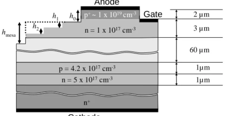
Structure and Layout. The employed p+np-pn structure shown in Fig. 1 is typical for asymmetric SiC GTO thyristors. The five epilayers were grown on an 8°-off n-type 4H-SiC wafer from Cree, Inc. With 3 µm, the n-base layer is relatively thick, since originally the wafer (without
p+ anode epi-layer) was designated for planar thyristors with an implanted anode [6]. As in [5] the
n-base layer was used to form a 3-step JTE at the periphery of the devices on one sample (no. 2). On the other sample (no. 1) the devices are terminated by a single mesa etch, which is equivalent to a single step JTE. The critical forward breakdown voltage of the plane-parallel junction, simulated
with the T-CAD software SentaurusTM and using the ionization coefficients from [8], amounts to
The devices layout shown in Fig. 2 reveals the three 50 µm wide JTE steps surrounding the active area. Discernible is the second metallization level which consists of a gate stripe in the middle of two bigger anode contacts areas. While the gate stripe is necessary to interconnect the gate fingers by feedthroughs, the anode fingers are already interconnected by the first metallization level underneath the passivation layer. The gate and anode fingers have equal width of 30 and
60 µm, respectively. The active devices area is 4.8610-3
cm2 for all devices considered in this
paper. n = 1 x 1017cm-3 p+ ~ 1 x 1019 cm-3 n = 5 x 1017cm-3 P-= 9,7·1014cm-3 n+ p = 4.2 x 1017cm-3 Anode Gate Cathode 2 µm 3 µm 60 µm 1µm 1µm hmesa h0 h1 h2 anode gate JTE steps
Fig. 1: Schematic cross-section of the employed thyristor structure with GEJTE.
Fig. 2: Top view of a fabricated SiC GTO
thyristor die (1.4 by 1.4 mm2) with an etched
3-step JTE.
Processing. The two samples considered in this paper have been processed together. Each
sample is about 1 cm2 in size and comprises more than 30 GTO thyristors with identical footprint
(Fig. 2). A set of seven masks was used to fabricate the devices. All etching steps were done with a
reactive ion etching (RIE) process. First, the gate/anode structure (h0) was etched to a depth of
3.9 µm using a nickel mask. Despite of possible metal contaminations this was done for reasons of
selectivity and lateral resolution. The following etching steps for the mesa (hmesa) and the JTE were
done using photo resist masks. Initially, the mesa was defined by an etching of 2.2 µm. During the subsequent two etching runs, on one sample, the mesa was protected the same way, and on the
other, smaller masks were used to define the two additional JTE steps, h1 and h2, finally measuring
390 nm and 426 nm, respectively. Thus, the total mesa height is identical on both samples and amounts to approximately 3 µm.
After etching the samples were thoroughly cleaned and then ohmic contacts were realized separately for surfaces on n- and p-type SiC. For the contacts on the gate and the cathode, Ni was used and annealed at 1100°C. For the contacts on the anode, a Ni/Ti/Al tri-layer was used and
annealed at 850°C. Thereafter a 1 µm thick Al based over-metallization was formed. Next, SiO2
was deposited by PECVD to passivate the surface and to isolate the first from the second metallization level. After oxide opening, a second metallization level was formed with Al as shown in Fig. 2.
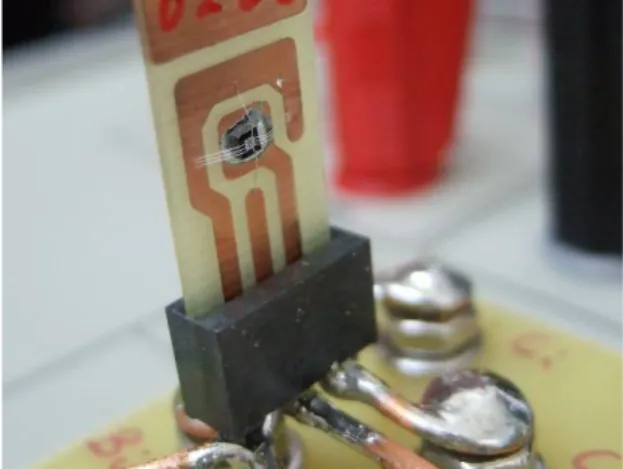
Packaging. After front end processing and preliminary electrical characterization, the two
samples have been cut into dies measuring 1.4 by 1.4 mm2 (Fig. 2). Some of these dies have then
been attached to a PCB type of support to facilitate the electrical connection of the three electrodes. While the cathode contact was soldered, the upper contacts have been bonded using 50 µm Al wires, a single one for the gate and up to three on each anode pad. The final packaging, which does not yet use any encapsulation, is shown in Fig. 5.
Electrical Characterization
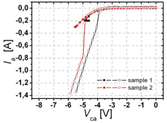
Blocking Characteristics. The blocking capability of the devices has been measured before dicing
characteristics of those 5 thyristors on each sample presenting the highest blocking voltages are shown in Fig. 3. Obviously, the best thyristors with GEJTE have a distinctively higher forward breakdown voltage and a slightly lower leakage current level than their counterparts with just a single step termination. For both types of devices, up to about -2 kV the leakage current rests below
the detection limit (10-10 A) of the measuring instrument.
The highest forward breakdown voltage amounts to 6 kV, which is just 75 % of the ideal value.
This is most likely to be explained by the two lower JTE steps (h1 and h2) being too high and thus
lowering the JTE dose too much. The gain of these two steps inherently depends on the initial JTE
dose, defined by h0, which is intentionally chosen higher than the optimal value. The breakdown
voltage limit of 4 kV, presented by devices with just a mesa etch, indicates that already the first JTE
step h0, defining this initial dose, is merely 100 nm lower than the value which is necessary to arrive
at an optimal dose of about 11013
cm-2. Therefore, it is likely that the subsequent JTE steps
overshoot the mark and could not optimally contribute to increase the termination efficiency.
Fig. 3. Comparison of the forward and reverse blocking characteristics of asymmetric SiC GTO thyristors with single step termination
(sample 1) and with a 3-step GEJTE
(sample 2).
Fig. 4. On-state characteristics of the
fabricated SiC thyristors measured with an SMU before (full symbols) and with a curve tracer after dicing and bonding (open symbols).
On-state Characteristics. On-state characteristics of devices from the two samples are shown in
Fig. 4. In each case two curves are depicted: one (full symbols) taken before dicing, using a probe station and an SMU, and another one (open symbols) originating from a bonded die measured with a curve tracer (Fig. 5). As expected, before dicing thyristors on both samples show a comparable on-state voltage drop. The obvious discrepancy for the two packaged devices is most likely attributed to problems with the anode bonding connection and not to differences in the termination.
The maximum current of roughly 1.4 A corresponds to a current density of 288 A/cm2 in the active
area of the device. The application of this load did not reveal any obvious stability problems.
Switching Characteristics. Fig. 6 shows switching characteristics of the same two bonded SiC
thyristor dies of which Fig. 4 depicts the on-state characteristics measured with a curve tracer.
Given are the waveforms of the anode current Ia, the cathode anode voltage Vca, and the gate current
Ig. The limitations of these first dynamic characteristics concerning the on-state current (100 mA)
and the blocking voltage (500 V) were due to both precaution and the used test set-up. The gate pulse applied in the experiments depicted in Fig. 6 was adjusted so that switching on and off were only just possible. The gate pulse width was set to 500 ns for turn-on and 10 µs for turn-off. For both devices a current of at least 15 mA and 30 mA was necessary to initiate on and gate turn-off, respectively. The overshot of the gate current in case of sample 2 is attributed to a current path parallel to the anode gate diode, probably originating from isolation problems caused by wire bonding. The turn-on delay time was 350 ns and 1.1µs for sample 1 and 2, respectively. For a gate current of 30 mA the turn-off delay amounted to 3.8 µs and 1 µs for sample 1 and 2, respectively.
Fig. 5: SiC GTO thyristor with a 3-step JTE attached to a PCB based package and bonded with 50 µm Al wires.
Fig. 6: Switching waveforms of bonded SiC thyristor dies originating from the two samples under investigation.
Conclusions
In conclusion, asymmetric SiC GTO thyristors with two differently etched terminations have been fabricated based on an epiwafer with a 60 µm drift layer. Thyristors terminated with a 3-step JTE show a forward blocking voltage of up to 6 kV, which is distinctively higher than the maximum value of equally processed devices with a single step termination. The termination efficiency of the 3-step JTE reaches just 75 % which is attributed to a deficiency of the applied etching process. Apart from that, the breakdown voltage of thyristors with a single step termination corresponds quite well to the expected value of 4 kV. Both types of devices show comparable on-state and switching characteristics. The on-state voltage drop is in the order of 5 V for a current density of
100 A/cm2, which is comparable to SiC thyristors with an implanted termination. The devices can
be switched on and off using reasonable gate pulses. The noticeable differences observed in the turn-off characteristics of the two specific devices depicted in this paper do rather result from processing defects than from differences in their termination. More experiments are necessary to evaluate the dynamic behavior and the switching capabilities of the devices.
References
[1] S. Scharnholz, B. Vergne, J.-P. Konrath, G. Pâques, and V. Zorngiebel, Pulse current characterization of SiC GTO thyristors, Material Science Forum 679-680 (2011) 682.
[2] A.K. Agarwal, C. Capell et al., 9 kV, 1 cmx1 cm SiC super GTO technology development for pulsed power, Proc. of Int. IEEE Pulsed Power Conference (2009) 264.
[3] X. Xu et al., Proc. of Power Electronics Specialists Conference, pp. 1 – 5, (2006)
[4] R. Ghandi et al., Implantation-free low on-resistance 4H-SiC BJTs with common emitter cur-rent gain of 50 and high blocking capability, Materials Science Forum 615-617 (2009) 833. [5] G. Pâques, N. Dheilly, D. Planson, R.W. De Doncker, and S. Scharnholz, Graded etched
junction termination for SiC thyristors, Materials Science Forum 679-680 (2011) 457.
[6] P. Brosselard, Conception, réalisation et caractérisation d’interrupteurs (thyristors et JFETs) haute tension (5 kV) en carbure de silicium, PhD dissertation, INSA de Lyon, 2004.