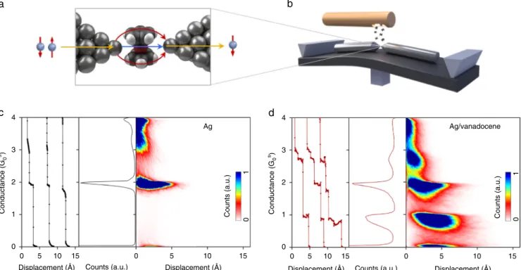
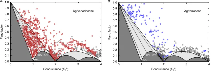
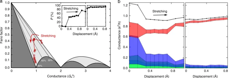
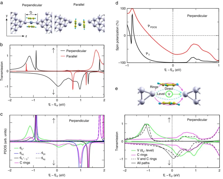
Nonmagnetic single-molecule spin-filter based on quantum interference
Texte intégral
Figure
Documents relatifs
First description of a new uncultured purple sulfur bacterium colonizing marine mangrove sediment in the Caribbean: Halochromatium-like PSB from Guadeloupe.. Olivier Gros,
Shkalla më e ulët e aktivitetit tek përfituesit e re- mitancave mund të jetë për shkak se pranuesit e papunë të dekurajuar kanë humbur shpresën për të gjetur
In this section, we present four simple possible tracking modes that all use as input the instrument’s localization method and robot control presented in the previous section. It
Inspired by the importance of latent variable initialization for VAE-based speech enhancement, and as another way than simple concatenation to effectively fuse audio and
Stefan Thiele. Read-out and coherent manipulation of an isolated nuclear spin using a single molecule magnet spin transistor. Quantum Physics [quant-ph]. Université de Grenoble,
39 National Research University Higher School of Economics, Moscow, Russia 40 Budker Institute of Nuclear Physics (SB RAS), Novosibirsk, Russia 41 Institute for High Energy
However, when performed at sufficiently high pressure and temperature close to the melting point of the wax (65°C and 30 MPa), similar debinding rate to the organic solvent immersion
In summary, this work demonstrates for the first time that in normal, nontransformed renal tubule, 1) glucose shortage increases VEGFA mRNA and protein levels in spite of high
