Electronic and structural properties of wurtzite III-V and II-VI
structures
Y. Al-Douria,*
, H. Khachaib, R. Khenatac, A. Addoub
aLaboratoire CRISMAT, ENSICAEN/CNRS UMR 6508, 6 boulevard du Maréchal Juin, F-14050 Caen Cedex, France. bApplied Materials Laboratory, University of Sidi Bel Abbes, 22000-Algeria.
cLaboratoire de Physique Quantique et de Modélisation Mathématique (LPQ3M), Département de Technologie, Université de
Mascara, 29000-Algeria.
*To whom correspondence should be addressed. E-mail: yaldouri@yahoo.com
Received 12 September 2007
ABSTRACT
The electronic and structural properties of wurtzite InN, ZnS and CdSe structures are studied using the empirical pseudopotential method (EPM). The principal energy at Γ of wurtzite InN, ZnS and CdSe compounds are calculated. Band structure of wurtzite InN, ZnS and CdSe materials are presented. Other quantity such as bulk modules by means of our model is calculated.
| III-V and II-VI structures | EPM | Wurtzite |
1. Introduction
The semiconductors have received considerable attention for their possible use in double heterostructure (DH) blue laser diodes (LDs) [1–5]. However, it remains a problem in searching for suitable cladding layer material that has energy gap (0.3 eV) higher than that of the active layer such as ZnTe [6,7]. To provide basis for understanding future device concepts and applications, we have computed the electronic properties of wurtzite compounds. The self-consistent pseudopotential method in the local density approximation usually underestimates the band gap and does not give the correct value for the effective mass [8,9]. The linear muffin-tin orbital (LMTO) method [9] is reliable but it is time consuming for computation of semiconductor compounds. Therefore, we have employed the empirical pseudopotential method (EPM) [10]. In this method, the actual atomic potential is replaced by pseudopotential and set of atomic form factors are adjusted so that the calculation produces the energy bands as accurately as possible in overall comparison with the existing experimental data.
Article
J
ournal of
F
undamental
S
ciences
Available online at http://www.ibnusina.utm.my/jfs http://dx.doi.org/10.11113/mjfas.v3n2.31Y. Al-Douri et al. / Journal of Fundamental Sciences 3 (2007) 225-231 226
This method is simple and is expected to give quick and reliable results which will be valuable for the assessment of the intrinsic and extrinsic material phenomena to determine the properties for optoelectronic devices applications. In this paper, we show band structures and pseudopotential form factors for wurtzite InN, ZnS and CdSe structures. The calculated results of energy gap and the effective lattice constant are presented. By the way, we have used this procedure for testing the validity of our model [11] of bulk modulus. In the subsequent section a brief description of the used method is presented. The calculated results and discussion are presented in Sec. 3. The last section consists of conclusion.
2. Pseudopotential calculation
At the present work the EPM electronic band structure as well as corresponding set of k.p parameters for wurtzite InN, ZnS and CdSe crystals have been studied. The pseudopotential Hamiltonian is given by
H=−∇
r
2+VPS(rv), (1)where VPS is the pseudopotential that can be expanded in reciprocal lattice vectors G
v as: =
∑
G r G i PS e V r V G v v v v v) ( ) . ( . (2)For the wurtzite structures the matrix elements of the crystal pseudopotential appears as [12]
V(G G) VS( 2)SS(G G) iVA( 2)SA(G G′) − + ′ − = ′ − v v v v v v (3) where VS and
VA are the symmetric and antisymmetric form factors, and
SS and
SA are the symmetric and antisymmetric structure factors specific to the wurtzite crystals, respectively.
More detail (G )=1
∑
(−G. ), λ λ τv r r exp n SS =−∑
− λ λ λ τ ) . G ( P ) G (r exp r v n i SA (4) G Gv− v′ Gv−Gv′Y. Al-Douri et al. / Journal of Fundamental Sciences 3 (2007) 225-231 227
where n is number of atoms per unit cell (at wurtzite structure n=4),
τ
v
λ is the basis vector of λth atom at the unit cell and λ indicate the type of atom I or II.where
−
+
=
II
type
atom
1
I
type
atom
1
λP
(5) λτ
r
localizes the position of the four atoms at the unit cell to format the cell − − − − = − + = 2 4 1 , 6 1 , 6 1 2 4 1 , 6 1 , 6 1 2 1 u u τ τ r r
Localized vector of the two atoms of type I
−
=
=
1 4 2 3τ
τ
τ
τ
r
r
r
r
Localized vector of the two atoms of type II and
[
(r ) (r)]
( G.r ) r 2 1 ) G ( 3 2 1 r r r r r r d i exp v v n VS + − Ω =∫
[
(r ) (r)]
( G.r ) r 2 1 ) G ( 3 2 1 r r r r r r d i exp v v n VA − − Ω =∫
(6)where Ω is the volume of the unit cell.
3. Results and discussion 3.1. Electronic band structure
In the wurtzite structure we have four atoms in the unit cell so that we have eight valence bands. We notice that bands 1 and 2 are very s-like whereas the rest of the bands have pronounced p-like character. In particular bands 6 and 8 are almost pure pxy-like and pz-like respectively. We also notice that the character of the conduction band
Y. Al-Douri et al. / Journal of Fundamental Sciences 3 (2007) 225-231 228
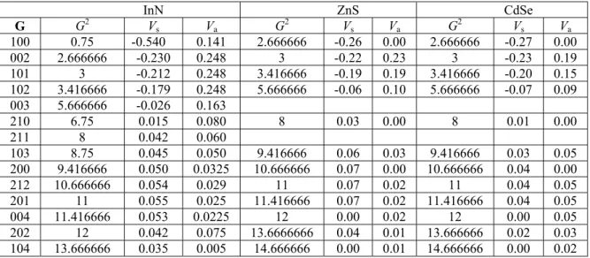
Table 1. The reciprocal lattice vectors and adjusted symmetric and antisymmetric form factors of wurtzite InN,
ZnS and CdSe structures in (Ry).
InN ZnS CdSe G G2 V s Va G2 Vs Va G2 Vs Va 100 0.75 -0.540 0.141 2.666666 -0.26 0.00 2.666666 -0.27 0.00 002 2.666666 -0.230 0.248 3 -0.22 0.23 3 -0.23 0.19 101 3 -0.212 0.248 3.416666 -0.19 0.19 3.416666 -0.20 0.15 102 3.416666 -0.179 0.248 5.666666 -0.06 0.10 5.666666 -0.07 0.09 003 5.666666 -0.026 0.163 210 6.75 0.015 0.080 8 0.03 0.00 8 0.01 0.00 211 8 0.042 0.060 103 8.75 0.045 0.050 9.416666 0.06 0.03 9.416666 0.03 0.05 200 9.416666 0.050 0.0325 10.666666 0.07 0.00 10.666666 0.04 0.00 212 10.666666 0.054 0.029 11 0.07 0.02 11 0.04 0.05 201 11 0.055 0.025 11.416666 0.07 0.02 11.416666 0.04 0.05 004 11.416666 0.053 0.0225 12 0.00 0.02 12 0.00 0.05 202 12 0.042 0.075 13.6666666 0.04 0.01 13.666666 0.02 0.03 104 13.666666 0.035 0.005 14.666666 0.00 0.01 14.666666 0.00 0.02
Table 2. The calculated band gaps along Γ→Γ in (eV) compared with theoretical and experimental ones of
wurtzite InN, ZnS and CdSe structures.
EgΓΓ InN ZnS CdSe
Cal. 2.27 3.80 1.96
Theo. 1.02a, 2.04b 3.35a 1.79a
Exp. 1.90c, 2.2d, 2.05e 3.91f 1.84g, 1.80f
a: Ref. [13], b: Ref. [14], c: Ref. [15], d: exp. Ref. [16], e: Ref. [17], f: Ref. [18], g: Ref. [19].
Table 3. The calculated and experimental lattice constants in (Å). For wurtzite structure we give the effective
cubic lattice constant defined through
a
eff3=
3
a
2c
[16] with the calculated, theoretical and experimentalbulk moduli in (GPa) of wurtzite InN, ZnS and CdSe structures.
InN ZnS CdSe a cal. 6.6764 7.2075 8.1239 a exp. 4.94a 5.359a 6.04a Bo cal. 137.92 103.91 68.17 Bo theo. 212a, 166b 50a 58a Bo exp. 125.5c 78d, 76.2e 53d
Y. Al-Douri et al. / Journal of Fundamental Sciences 3 (2007) 225-231 229 -20 -15 -10 -5 0 5 10 15 20 Γ K H A M L A Γ Wurtzite InN Ene rgy (eV) Wave vector -15 -10 -5 0 5 10 15 K H Γ Γ M L A A Wurtzite ZnS En er gy ( e V ) Wave vector -15 -10 -5 0 5 10 15 Γ K H A M L A Wurtzite CdSe Γ Energy (eV ) Wave vector
Fig. 1 Calculated band structure of wurtzite InN (a) Calculated band structure of wurtzite ZnS (b) Calculated
band structure of wurtzite CdSe (c). (a)
(b)
Y. Al-Douri et al. / Journal of Fundamental Sciences 3 (2007) 225-231 230
The pseudopotential form factors for the wurtzite InN, ZnS and CdSe crystals are shown in table 1. They give the reasonable agreement with experiment and other calculations for the principal energy gap along Γ→Γ (see Table 2). In Fig. 1, one can show the calculated band structure of InN, ZnS and CdSe compounds. The band structure is typical of the wurtzite structure. The compounds exhibit a direct gap for the given structures.
3.2. Bulk modulus calculation
An important observation for studying B0 is the clear differences between the lattice constant in going from the
group III–V and II–VI semiconductors as seen in table 3. One can view the effect of increasing covalency. As the covalency increases, the pseudopotential becomes more attractive and pulls the charge more toward the core region, hence reducing the number of electrons available for the chemical bonding. The modulus generally increases with the covalency but not as fast as predicted by the uniform density term. The lattice constants are predominantly dependent on B0 where impetus us to applicable study between the two and to test the validity of
our empirical model [11] by a new parameterization of bulk moduli. − − = 2 5 . 3 0 [3000 100] a B λ (7)
where a is the lattice constant in (Å) and λ is an empirical parameter which accounts λ = 0, 1, 2 for group IV, III– V, and II–VI semiconductors, respectively, 2 in (Å) and the first term in (GPa). The calculated bulk modulus values compared with those of experimental and theoretical as given in table 3. The results of our calculations are in reasonable agreement with experimental and theoretical ones except for ZnS where the emergence is happened.
4. Conclusion
Electronic band structures of wurtzite InN, ZnS and CdSe structures are calculated using empirical pseudopotential method. It is shown that these structures have direct gap. The results of the bulk moduli are calculated. A reasonable agreement with experimental and theoretical data was observed.
References
[1] H. Jeon, J. Ding, A. V. Nurmikko, H. Luo, N. Samarth, J. K. Fyrdyna, and W. A. Bonner, Appl. Phys. Lett.
57, 2413, 1990.
Y. Al-Douri et al. / Journal of Fundamental Sciences 3 (2007) 225-231 231
[3] S. Fujita, S. Hayashi, M. Funato, T. Yoshte, and S. Fujita, J. Cryst. Growth 107, 674, 1991. [4] M. A. Hasse, J. Qiu, J. M. DePuydt, and H. Cheng, Appl. Phys. Lett. 59, 1272, 1991. [5] G. Sun, K. Shahzad, J. M. Gaines, and J. B. Khurgin, Appl. Phys. Lett. 59, 310, 1991.
[6] H. Okuyama, K. Nakano, T. Miyajima, and K. Akimoto, Jpn. J. Appl. Phys., Part 2 30, L1620, 1991. [7] H. Okuyama, K. Nakano, T. Miyajima, and K. Akimoto, J. Cryst. Growth 117, 139, 1992.
[8] J. Serrano, A. Rubio, E. Hernandez, A. Munoz, A. Mujica, Phys. Rev. B 62, 16612, 2000.
[9] K. Lawniczak-Jablonska, T. Suski, I. Gorczyca, N. E. Christensen, K. E. Attenkofer, R. C. C. Perera, E. M. Gullikson, J. H. Underwood, D. L. Ederer, Z. Liliental Weber, Phys. Rev. B 61, 16623, 2000.
[10] M. L. Cohen and T. K. Bergstresser, Phys. Rev. 141, 789, 1966. [11] Y. Al-Douri, H. Abid, H. Aourag, Mater. Chem. Phys. 87, 14, 2004.
[12] M.L. Cohen, J.R. Chelikowsky, Electronic structure and optical properties of semiconductors, Springer, New York, 1989.
[13] Y-N. Xu and W. Y. Ching, Phys. Rev. B 48, 4335, 1993.
[14] S. N. Grinyaev, V. Ya. Malakhov, V. A. Chaldyshev, Izv. Vyssh. Uchebn. Zaved. Fiz. 4, 69, 1986. [15] R. B. Zetterstram, J. Mater. Sci. 5, 1102, 1970.
[16] N. E. Christensen, I. Gorczyca, Phys. Rev. B 50, 4397, 1994.
[17] W. A. Tyagay et al. Fiz. Tekh. Poluprovodn. 11, 2142, 1977 [Sov. Phys. Semicond. 11, 1257, 1977. [18] Handbook of laser science and technology, edited by M. J. Weber (CRC, Cleveland, 1986), Vol. III. [19] L. Ley. R. A. Pollak, F. R. McFeely, S. P. Kowalczyk, D. A. Shireley, Phys. Rev. B 9, 600, 1974.
[20] P. E. Van Camp, V. F. Van Doren, J. T. Devreese, Phys. Rev. B 44, 9056, 1991; Solid State Commun. 81, 23, 1992.
[21] C. F. Cline, D. R. Stephens, J. Appl. Phys. 36, 2869, 1965. [22] E. Chang, G. R. Barsch, J. Phys. Chem. Solids 34, 1543, 1973.