HAL Id: tel-03121111
https://tel.archives-ouvertes.fr/tel-03121111
Submitted on 26 Jan 2021HAL is a multi-disciplinary open access
archive for the deposit and dissemination of sci-entific research documents, whether they are pub-lished or not. The documents may come from teaching and research institutions in France or abroad, or from public or private research centers.
L’archive ouverte pluridisciplinaire HAL, est destinée au dépôt et à la diffusion de documents scientifiques de niveau recherche, publiés ou non, émanant des établissements d’enseignement et de recherche français ou étrangers, des laboratoires publics ou privés.
compact model operating close to safe operating area
edges
Marine Couret
To cite this version:
Marine Couret. Failure mechanisms implementation into SiGe HBT compact model operating close to safe operating area edges. Electronics. Université de Bordeaux, 2020. English. �NNT : 2020BORD0265�. �tel-03121111�
THÈSE PRÉSENTÉE POUR OBTENIR LE GRADE DE
DOCTEUR DE L’UNIVERSITÉ DE BORDEAUX
ÉCOLE DOCTORALE DES SCIENCES PHYSIQUES ET DE L’INGÉNIEUR SPÉCIALITÉ ÉLECTRONIQUE
présentée et soutenue publiquement par
Marine COURET
le 15 décembre 2020
FAILURE
MECHANISMS
IMPLEMENTATION INTO
SIGE
HBT COMPACT
MODEL
OPERATING CLOSE TO
SAFE-OPERATING-A
REAE
DGESDirectrice de thèse : Cristell MANEUX
Membres du jury :
M. ANIELFrédéric, Professeur, C2N, Université Paris-Sud Rapporteur
M. PASCALFabien, Professeur, IES, Université de Montpellier Rapporteur
M. CÉLIDidier, Ingénieur, STMicroelectronics Examinateur
Mme DELTIMPLENathalie, MCF HDR, IMS, Bordeaux INP Examinatrice
M. FISCHERGerhard, Ingénieur, IHP Microelectronics Examinateur
M. MARCFrançois, MCF HDR, IMS, Université de Bordeaux Examinateur
M. BEGUERETJean-Baptiste, Professeur, IMS, Université de Bordeaux Président
Mme MANEUXCristell, Professeur, IMS, Université de Bordeaux Directrice de thèse
Université de Bordeaux
Laboratoire de l’Intégration du Matériau au Système
i
Abstract - EN
In an ever-growing terahertz market, BiCMOS technologies have reached cut-off frequencies beyond 0.5 THz. These dynamic performances are achieved thanks to the current technologi-cal improvements in SiGe hetero-junction bipolar transistors (HBTs). However, these increased performances lead to a shift of the transistors bias point closer to, or even beyond, the con-ventional safe-operating-area (SOA). As a consequence, several parasitic physical effects are encountered such as impact-ionization or self-heating which can potentially activate failure mechanisms, hence limiting the long-term reliability of the electronic device. In the frame-work of this thesis, we develop an approach for the description and the modeling of hot-carrier degradation occurring in SiGe HBTs when operating near the SOA edges. The study aims to provide an in-depth characterization of transistors operating under static and dynamic op-erating conditions. Based on these measurements results, a compact model for the impact-ionization and the self-heating has been proposed, ultimately allowing to extend the validity domain of a commercially available compact model (HiCuM). Considering the operation as close as possible to the SOA, an aging campaign was conducted to figure out the physical origin behind such failure mechanism. As a result, it has been demonstrated that hot-carrier degra-dation leads to the creation of trap densities at the Si/SiO2interface of the emitter-base spacer
which induces an additional recombination current in the base. A compact model integrating aging laws (HiCuM-AL) was developed to predict the evolution of the transistor/circuit elec-trical parameters through an accelerated aging factor. For ease of use in computer-aided design (CAD) tools, the aging laws have been scaled according to the geometry and architecture of the emitter-base spacer. The model has demonstrated its robustness and its accuracy for different SiGe HBT technologies under various aging conditions. In addition, a study on the reliability of several integrated circuits has been performed leading to a precise location of the most sensi-tive regions to the hot-carrier degradation mechanism. Thus, the HiCuM-AL model paves the way to perform circuit simulations optimizing the mm-wave circuit design not only in terms of sheer performances but also in terms of long-term reliability.
iii
Résumé - FR
Afin de répondre au marché florissant des applications térahertz, les filières BiCMOS atteignent désormais des fréquences de coupure supérieures à 0,5 THz. Ces performances dynamiques sont obtenues grâce aux améliorations technologiques apportées aux transistors bipolaires à hétérojonction (TBH) SiGe. Toutefois, cette montée en fréquence à entraîner un décalage du point de polarisation des transistors au plus proche, voir au-delà, de l’aire de sécurité de fonc-tionnement (SOA). En conséquence, de nombreux effets physiques parasites sont déclenchés tel que l’ionisation par impact ou bien l’auto-échauffement pouvant potentiellement activer des mécanismes de défaillance et ainsi limiter la fiabilité à long terme du transistor. Dans le cadre de cette thèse, nous proposons une approche pour la description et la modélisation de la dégradation par porteurs chauds au sein des TBH SiGe fonctionnant aux frontières de la SOA. L’étude est basée sur une caractérisation approfondie en conditions statiques et dynamiques des transistors. Du fait de ses résultats de mesures, une modélisation de l’ionisation par im-pact et de l’auto-échauffement a été proposé permettant d’étendre, avec précision, le domaine de validité des modèles compact commerciaux (HiCuM). Au-vu du fonctionnement aux limites de la SOA, une campagne de vieillissement a été mise en place afin de mieux cerner l’origine physique de ce mécanisme de défaillance. De ce fait, il a été démontré que la dégradation par porteurs chauds entraîne la création de densités de pièges au niveau de l’interface Si/SiO2 de
l’espaceur émetteur-base induisant un courant de recombinaison supplémentaire dans la base. Un modèle compact intégrant des lois de vieillissement (HiCuM-AL) a été développé prédisant l’évolution des paramètres électriques d’un transistor ou d’un circuit au travers d’un facteur de vieillissement accéléré. Afin de facilier son utilisation dans des outils de conception assistée par ordinateur (CAO), les lois de vieillissement ont été adaptées en fonction de la géométrie et de l’archictecture de l’espaceur émetteur-base. Le modèle a démontré sa robustesse et sa précision pour plusieurs technologies de TBH SiGe et, ce, pour différentes conditions de vieillissement. De plus, une étude de la fiabilité de plusieurs architectures de circuits intégrés a été réalisé menant à une localisation précise des régions les plus sensibles au mécanisme de dégradation par porteurs chauds. Le modèle HiCuM-AL ouvre ainsi la voie à des simulations optimisées pour la conception de circuits millimétriques en termes de performances, mais aussi de fiabilité à long terme.
v
Acknowledgments
Je souhaiterais tout d’abord remercier ma directrice de thèse, Dr Cristell Maneux, sans qui ce manuscrit n’aurait pas vu le jour. A coup de corrections roses, tu m’as donné l’envie, tout au long de cette thèse, de me surpasser et de produire un travail dont je suis fière. Merci !
Mes sincères remerciements vont au Dr François Marc et Dr Chhandak Mukherjee qui ont ardemment participé et contribué au succès de cette thèse. Au même titre, je tiens à présenter mes remerciements à Magali De Matos pour sa bienvieillance et son dynamisme. Tu as fait de la salle de caractérisation un lieu de partage et de convivialité.
A special thanks to Gerhard Fischer who was a great support from the beginning of this journey. I particularly appreciated our exchanges and your warm welcome during my visit to Frankfurt. I retain of this visit, an excellent souvenir.
Je tiens aussi à remercier les autres membres du groupe Nanoélectronique. Plus particulière-ment Dr Thomas Zimmer, pour sa justesse et ses conseils. Mais égaleparticulière-ment Dr Patrick Mounaix, pour nos échanges piquants, mais toujours respectueux (enfin, je crois).
Mes chaleureux remerciements au Dr Marina Deng qui m’a soutenu dans mes premiers pas dans l’enseignement. J’ai, grâce à toi, eu des opportunités que peu de doctorants ont la chance d’avoir. Merci au Dr Frédéric Darracq pour la supervision de mes enseignements à l’UF Sci-ences de l’Ingénieur. Je remercie aussi toute l’équipe pédagogique du CREEA qui m’a accom-pagné en tant qu’étudiante puis en tant qu’enseignante. Je pense notamment à Myriam, Luc, Didier, Stéphane et Xavier.
Une reconnaissance particulière au Dr Jean-Baptiste Begueret pour sa bienveillance durant ces dernières années. Je te remercie de m’avoir accompagné jusqu’à la fin de ce parcours en prési-dant ma soutenance de thèse.
Il ne me faut pas oublier mon collègue, mon coéquiper, mon compère d’aventure, le Dr Mathieu Jaoul. Comme tu l’as si bien écrit, nos thèses ont été étroitement liées soldant ainsi une solide amitié entre nous.
Mes pensées à ma seconde famille, mes amis, pour la plupart rencontrés tout au long de cette thèse ou lors de nos années d’étude. A toutes nos sorties, nos soirées, nos bouffes, nos es-capades, nos discussions, nos rires qui ont, à jamais, gravés dans ma mémoire de merveilleux souvenirs. Pour ses moments, je me dois de remercier Matthieu, Quentin, Ming Ming, Adrien, Margaux, Djeber, Jean-Baptiste, Marco, Florent M., Florent A., Nolwenn, Romain, Isabel, Olivia, Claire et Fanny.
Comment ne pas remercier Ghyslain, passé de camarade, voisin, collègue à meilleur ami. Mal-gré ton absence, tu n’as jamais manqué de me soutenir et de me conseiller dans mes périodes de doutes.
Je tiens aussi à remercier mes beaux-parents d’avoir fait de leur maison, un lieu où je pouvais me ressourcer. Merci également à Sonia, Adrien et l’espiègle Pénélope pour les bons moments passés en famille.
Mes pensées vont à mes parents, pour leur affection, leur confiance et leur support, sans lesquels, tout ce travail n’aurait jamais été réalisable. Il en va de même pour mes soeurs, Vir-ginie et Aurélie, pour qui je suis toujours une petite chipie.
Finalement, et non des moindes, j’aimerais exprimer ma reconnaissance à mon conjoint, Thomas, pour son affection, son empathie, sa patience et, surtout, son indéfectible soutien. Tel un super-héros, tu as su me préserver durant ces années et je te dois une grande partie de ma réussite.
vii
Contents
Abstract - EN i Résumé - FR iii Acknowledgments v List of Figures ixList of Tables xvii
General Introduction 1 1 State-of-the-art of SiGe HBTs 5 1.1 Introduction . . . 6 1.2 Terahertz radiations . . . 6 1.3 Technology . . . 9 1.4 Device operation . . . 14 1.5 Compact modeling . . . 19 1.6 Reliability issue . . . 21
1.7 Technologies under analysis . . . 23
1.8 Conclusion . . . 26
2 Compact Modeling of High Biases Mechanisms 27 2.1 Introduction . . . 28
2.2 Limitations of HiCuM compact model . . . 28
2.3 DC characterization of self-heating effect . . . 32
2.4 Compact modeling of avalanche effect . . . 36
2.5 AC characterization of self-heating effect . . . 43
2.6 Physics-based electrothermal compact model . . . 49
2.7 Time domain validation . . . 54
2.8 Conclusion . . . 58
3 Physics and Modeling of Hot-Carrier Degradation 61 3.1 Introduction . . . 62
3.2 Physics of hot-carrier degradation . . . 62
3.4 Compact modeling . . . 73
3.5 Scaled formulation . . . 81
3.6 Parameter extraction . . . 87
3.7 Simulation results . . . 91
3.8 Conclusion . . . 94
4 Hot-Carrier Degradation Impact on Integrated Circuits 97 4.1 Introduction . . . 98
4.2 Current mirrors . . . 98
4.3 Ring oscillator . . . 108
4.4 A test vehicle: a broadband amplifier . . . 113
4.5 Conclusion . . . 121
General Conclusion 123
Author Publication List 127
ix
List of Figures
1.1 Location of the terahertz radiations within the electromagnetic spectrum. . . 6 1.2 Atmospheric absorption as a function of the signal frequency taken from [4]. . . 7 1.3 Potential applications for silicon integrated mm-wave and THz circuits taken
from [5]. . . 8 1.4 Histology image and terahertz image of breast cancer taken from [20]. . . 9 1.5 Schematic cross-section of a high-speed SiGe HBT taken from [5]. . . 11 1.6 Schematic flow of the selective epitaxial growth of the base link region in both
DSPA (left) and EBL (right) processes taken from [22]. . . 12 1.7 Schematic cross section of an NSEG HBT with elevated extrinsic base (EEB)
re-gions taken from [5]. . . 13 1.8 Creation of electron-hole pairs within the BC-SCR due to the impact ionization
mechanism. . . 14 1.9 (a) IBand (b) M evolution according to VCBhighlighting the avalanche behavior. 15
1.10 Output characteristics under (a) a constant VBE bias and (b) a constant IB bias
with and without self-heating effect. . . 16 1.11 Evolution of the transit frequency according to the collector current depicting
the Kirk effect onset at high current densities. . . 16 1.12 (a) Forward Gummel and (b) output characteristic showing the quasi-saturation
effect taken from [21]. . . 17 1.13 (a) Influence of the measurements configurations on a HBT output characteristic
and (b) Device junction temperature for a constant VBEsetup. . . 18
1.14 Stable Operation Regime for a constant VBEsetup on a high-speed SiGe HBT. . . 19
1.15 Equivalent electrical circuit of HiCuM/L2 including the electro-thermal node. Not shown are the networks for NQS effects and correlated noise. . . 21 1.16 Safe Operating Area boundaries for a constant VBE setup on a high-speed SiGe
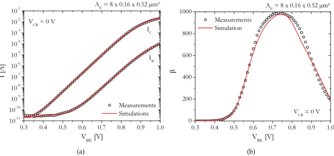
HBT. . . 22 1.17 Base current and current gain β as a function of VBEfor a mixed-mode stress of
VCB=3V and JE=0.12mA/µm2on a 8 x 0.16 x 0.52 µm2 device corresponding to
SG13S technology from IHP Microelectronics. . . 22 1.18 Methodology for circuit reliability prediction. . . 23 1.19 (a) ft and fmax as a function of the collector current and (b) Gummel
character-istics for a high-speed transistor corresponding to SG13S technology from IHP Microelectronics. . . 24
1.20 (a) Schematic [64] and (b) TEM cross-section [62] for a high-speed transistor from SG13S technology. . . 24 1.21 TEM cross-section of a 0.1 x 4.9 µm2HS SiGe HBT from B55 technology [23]. . . . 25
2.1 Comparison between measurements (symbols) and HiCuM/L2 simulation v2.34 (solid lines) for (a) the forward Gummel characteristic and (b) the current gain at VCB= 0 V on a 8 x 0.16 x 0.52 µm2device corresponding to SG13S technology
from IHP Microelectronics. . . 28 2.2 Comparison between measurements (symbols) and HiCuM/L2 v2.34 simulation
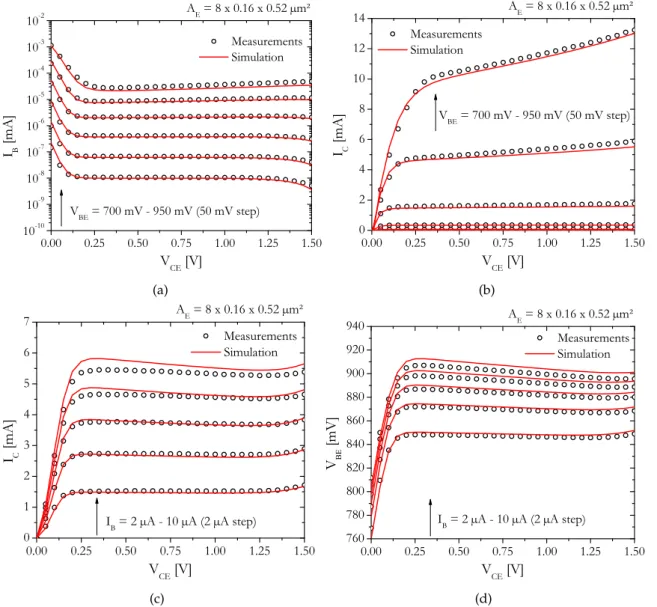
(solid lines) for (a) IBand (b) ICas function of VCEunder constant VBE’s bias and
for (c) IC and (d) VB as function of VCE under constant IB’s bias on a 8 x 0.16 x
0.52 µm2device corresponding to SG13S technology from IHP Microelectronics. 29 2.3 Comparison between measurements (symbols) and HiCuM/L2 simulation (solid
lines) for (a) fTand (b) fMAXas function of VBEat various VCE’s bias on a 8 x 0.16
x 0.52 µm2device corresponding to SG13S technology from IHP Microelectronics. 30
2.4 Comparison between measurements (symbols) and HiCuM/L2 simulation v2.34 (solid lines) for the multiplication factor, M, at (a) various VCBunder a constant
VBE and (b) various IE under constant VCB’s on a 8 x 0.16 x 0.52 µm2 device
corresponding to SG13S technology from IHP Microelectronics. . . 31 2.5 Comparison between measurements (symbols) and HiCuM/L2 simulation v2.34
(solid lines) for the thermal impedance (a) magnitude and (b) phase evolution according to the frequency on a 8 x 0.16 x 0.52 µm2 device corresponding to
SG13S technology from IHP Microelectronics. . . 32 2.6 Measurement results of (a) forward Gummel behavior illustrating the
intersec-tion technique and (b) corresponding juncintersec-tion temperature on a 8 x 0.16 x 0.52
µm2device corresponding to SG13S technology from IHP Microelectronics. . . . 33
2.7 Thermal resistance evolution according to (a) the device temperature and (b) the emitter area for SG13S technology from IHP Microelectronics. The extraction is performed based on the intersection technique. . . 35 2.8 Comparison between measurements (symbols) and compact model simulation
results (solid lines) of (a) HiCuM/L2 v2.34 (in red) and v2.4.0 (in blue) at VBE
= 0.6 V and (b) HiCuM/L2 v2.4.0 (in red) and v3.0.0 (in blue) at IE = 8 mA for
the base current and the multiplication factor on a 8 x 0.16 x 0.52 µm2 device
corresponding to SG13S technology from IHP Microelectronics. . . 38 2.9 Extraction flow the avalanche related parameters reproduced from [31]. . . 39 2.10 Illustration of the extraction (a) range and (b) methodology for the weak avalanche
parameters (fAVL and qAVL) on a 8 x 0.16 x 0.52 µm2 device corresponding to
SG13S technology from IHP Microelectronics. . . 40 2.11 Thermal coefficient extraction for (a) fAVLand (b) qAVL parameters for a 8 x 0.16
x 0.52 µm2device corresponding to SG13S technology from IHP Microelectronics. 40 2.12 (a) kAVL extraction result and (b) associated thermal coefficient for a 8 x 0.16 x
xi
2.13 Compact model simulations results (solid lines) vs measurements (symbols) for IB evolution according to VCB at (a) various VBE values, (b) various IE values,
(c) various TAMB and (d) various emitter dimensions corresponding to SG13S
technology from IHP Microelectronics. A current compliance is used to avoid the transistor destruction. . . 42 2.14 Low-frequency S-parameters measurement bench. . . 46 2.15 (a) Real and (b) imaginary part of Y22 with the corresponding extrapolation to
extract the isothermal values using a power function for a 8 x 0.16 x 0.52 µm2 device corresponding to SG13S technology from IHP Microelectronics. . . 46 2.16 Extraction results for (a) the magnitude and (b) the phase of ZTH for different
emitter geometries corresponding to SG13S technology from IHP Microelectronics. 47 2.17 Electrical equivalent circuit of the recursive electrothermal network. . . 47 2.18 Comparison between measurements (symbols) and recursive network
simula-tion (solid lines) for (a) the magnitude and (b) the phase of ZTH for different
emitter geometries corresponding to SG13S technology from IHP Microelectron-ics. . . 48 2.19 Illustration of the heat flow volume in a SiGe HBT architecture considering the
BEOL metal layers. Note that the heat source is assumed to be located at the base-collector junction and the contributions from the emitter and the neutral base are neglected. . . 49 2.20 Downward heat diffusion for (a) θ < θC and (b) θ > θCcorresponding to a half
cross-section corresponding to SG13S technology from IHP Microelectronics. . . 50 2.21 Electrical equivalent circuit of the downward heat flow for a SG13S technology
from IHP Microelectronics. . . 52 2.22 Electrical equivalent circuit of the physics-based electrothermal network. . . 53 2.23 Comparison between measurements (symbols) and physics-based
electrother-mal model simulation (solid lines) for (a) the magnitude and (b) the phase of ZTH for different emitter geometries corresponding to SG13S technology from
IHP Microelectronics. . . 54 2.24 Comparison between measurements (symbols) and physics-based
electrother-mal model simulation (solid lines) for Y12(a) magnitude and (b) phase, on a 8 x
0.16 x 0.52 µm2corresponding to SG13S technology from IHP Microelectronics. . 55
2.25 Comparison between measurements (symbols) and physics-based electrother-mal model simulation (solid lines) for Y22(a) magnitude and (b) phase, on a 8 x
0.16 x 0.52 µm2corresponding to SG13S technology from IHP Microelectronics. . 55 2.26 Experimental setup for pulse measurements. . . 56 2.27 (a) Equivalent circuit model of the coaxial cables consisting of passive elements,
the generator resistance RGand device open capacitance COPENand (b) Compact
model simulation results on the base and collector current using the coaxial cable model at VBE= 0.95 V and VCE= 1.5 V. . . 56
2.28 Collector current waveform (symbols) is compared to transient simulations (a) including the single pole (solid red lines) and the physics-based (solid blue lines) thermal model for a 8 x 0.16 x 0.52 µm2 device and (b) including the
physics-based (solid lines) thermal model for the four DUTs geometries corresponding to SG13S technology from IHP Microelectronics. Both figures are obtained at an operating condition of VBE= 0.95 V and VCE= 1.5 V. . . 57
3.1 (a) Si dangling bond creation at the Si/SiO2 interface, (b) Incorporation of
hy-drogen atoms for passivation of dangling bonds and (c) Interface trap carrier creation and hydrogen diffusion due to hot-carrier mechanism. . . 62 3.2 Schematic cross section of a SiGe HBT showing the Si/SiO2interfaces likely
sub-mitted to HCD. . . 63 3.3 (a) Forward and (b) Reverse Gummel characteristics with increasing mixed-mode
stress time (VCB= 2 V and JE= 0.35 mA/µm²) on a 0.42 x 5.56 µm² device
corre-sponding to B55 technology from ST Microelectronics. . . 64 3.4 Base current density evolution according to the PE/AE ratios extracted at VBE=
0.6 V and VBC= 0 V corresponding to B55 technology from ST Microelectronics. . 65
3.5 (a) Base current density as a function of the PE/AEratio for different stress
dura-tion extracted at VBE= 0.6 V and (b) Peripheral contribution of the base current
extracted from the slopes of figure 3.5a as a function of the stress duration at VBE
= 0.6 V corresponding to B55 technology from ST Microelectronics. . . 65 3.6 (a) Normalized peripheral part of the base current, IBPn, extracted from the
mea-surements in figure 3.3a for various stress duration and (b) IREpS evolution
ex-tracted from figure 3.6a with increasing mixed-mode stress time (VCB= 2 V and
JE = 0.35 mA/µm²) on a 0.42 x 5.56 µm² device corresponding to B55 technology
from ST Microelectronics. . . 66 3.7 TCAD structure of a B55 technology from ST Microelectronics showing the zoom
on the E-B spacer oxide where traps have been added at the Si/SiO2interface. . . 67
3.8 (a) TCAD simulation results for various trap densities and (b) corresponding JREpS evolution allowing to extract the proportionality coefficient α
representa-tive of the relationship between the density of defects at the interface and the base recombination current density value on a B55 technology from ST Micro-electronics . . . 68 3.9 Time-exponent evolution of JREpSparameter for a mixed-mode stress of VCB= 2
V and JE= 2.3 mA/µm² on a 0.2 x 5.56 µm² device corresponding to B55
technol-ogy from ST Microelectronics. . . 69 3.10 Relative base current evolution as a function of the stress duration for (a) VCB=
2.75 V and various JE and (b) JE= 0.12 mA/µm² and various VCBon a 8 x 0.16 x
xiii
3.11 Gummel characteristics (a) without any aging procedure and (b) after one hour of mixed-mode stress (VCB = 3 V and IE = 180 µA) at different ambient
temper-atures (-40°C;-10°C and 27°C) on a 8 x 0.16 x 0.52 µm² device corresponding to SG13S technology from IHP Microelectronics. . . 71 3.12 (a) Gummel characteristic and (b) relative base current evolution for a
mixed-mode stress (VCB = 2.7 V and IE = 20 mA) at high junction temperature (Tj =
315°C) applied on a 0.2 x 5.56 µm² device corresponding to B55 technology from ST Microelectronics. . . 71 3.13 Gummel characteristics before/after an annealing treatment at 125°C on a
for-mer aged transistor corresponding to SG13S technology from IHP Microelec-tronics. . . 72 3.14 (a) Bias conditions for dynamic mixed-mode stress and (b) relative base current
evolution for this particular stress mode compared to a DC mixed-mode stress on a 8 x 0.16 x 0.52 µm² device corresponding to SG13S technology from IHP Microelectronics. . . 73 3.15 Comparison between measurements (symbols) and simulations (solid line) of
the aging model proposed in [54] for a dynamic stress on a 8 x 0.16 x 0.52 µm² device corresponding to SG13S technology from IHP Microelectronics. . . 74 3.16 Implementation schematic of the reaction-diffusion model. . . 75 3.17 Schematic of the hydrogen diffusion considering the creation of traps at the
Si/SiO2interface. . . 76
3.18 Bode-like representation of normalized admittance ˜Y(0, f) =φ˜H(0, f)/ ˜NH(0, f)
of diffusion for the three cases of second interface properties. . . 78 3.19 Architecture of the R-C ladder model of diffusion equation system. . . 78 3.20 Bode-like representation of normalized admittance ˜Y(0, f) =φ˜H(0, f)/ ˜NH(0, f)
of the R-C ladder model for αR=4 and N=5 compared to the semi-infinite theory. 80
3.21 Comparison between measurements (symbols) and simulations (solid line) of the previous [54] and newly proposed [115] aging compact model for a dynamic stress on a 8 x 0.16 x 0.52 µm² device corresponding to SG13S technology from IHP Microelectronics. . . 81 3.22 Side view of the E-B spacer corresponding to B55 technology transistor
architec-ture from ST Microelectronics. . . 82 3.23 (a) Extracted IREpS parameter and (b) Calculated NT following equation (3.8)
from Gummel measurements for a stress condition of VCB = 2.4 V and JE = 231
µA/µm² and for three B55 technology devices from ST Microelectronics. . . 83 3.24 Schematic of the hydrogen diffusion volume taking into account the E-B spacer
oxide and the emitter poly-Si thickness for B55 technology from ST Microelec-tronics. . . 84 3.25 R-C ladder network for hydrogen diffusion modeling. . . 85
3.26 Bode-like representation of normalized admittance ˜Y(0, f) =φ˜H(0, f)/ ˜NH(0, f)
of the R-C ladder model for N = 3, G = 1/RN and various recursive factors α
compared to the semi-infinite theory. . . 86 3.27 Evolution of JREpSfor a static condition of VCB = 2 V and JE = 2.3 mA/µm² on a
0.2 x 5.56 µm² device corresponding to B55 technology from ST Microelectronics. The data were fitted with a three poles exponential decay function to extract the density of Si-H bonds at the interface, NF. . . 87
3.28 KF extraction example for a static stress condition of VCB = 2 V and JE = 4.6
mA/µm² on a 0.2 x 5.56 µm² corresponding to B55 technology from ST Micro-electronics. . . 89 3.29 (a) JC - VCB curves illustrating the stress conditions for KF extraction and (b)
KFextraction results with corresponding linear fit leading to equation (3.38) for
five stress conditions (see figure 3.29a) on a 0.2 x 5.56 µm² corresponding to B55 technology from ST Microelectronics. . . 90 3.30 KRextraction results for a 0.2 x 5.56µm² device corresponding to B55 technology
from ST Microelectronics. The data are fitted with an Arrhenius law. . . 91 3.31 HiCuM-AL v3.0 simulations (lines) vs measurements (symbols) for IREpS
evolu-tion according to the stress duraevolu-tion at (a) various stress condievolu-tions (see figure 3.29a), (b) various LE, (c) various WEand (d) Gummel evolution for a static stress
condition of VCB = 2 V and JE = 4.6 mA/µm² on devices corresponding to B55
technology from ST Microelectronics. . . 92 3.32 HiCuM-AL v3.0 simulations (lines) vs measurements (symbols) for IB evolution
according to the stress duration at (a) various VCB, (b) various JE, (c) under a
dynamic stress condition and (d) Gummel Gummel evolution for a static stress condition of VCB = 3 V and JE = 0.12 mA/µm² on a 8 x 0.16 x 0.52 µm² device
corresponding to SG13S technology from IHP Microelectronics. . . 94 4.1 Schematic of (a) the simple, (b) the cascode, (c) the Wilson and (d) the balanced
Wilson current mirrors. . . 99 4.2 Transfer ratio evolution for VOUT= 1.5 V according to (a) the input current and
(b) the frequency at II N = 100 µA. . . 101
4.3 (a) Input voltage evolution according to the input current for VOUT = 1.5 V and
(b) Input resistance evolution according to the frequency for VOUT = 1.5 V and
II N = 100 µA. . . 102
4.4 (a) Output current evolution according to the output voltage for II N = 100 µA
and (b) Output resistance evolution according to the frequency for VOUT= 1.5 V
and II N= 100 µA. . . 102
4.5 ICvs VCEoutput characteristics highlighting the transistors operating conditions
for each current mirror configurations at VOUT= 1.5 V and II N = 100 µA. . . 104
4.6 (a) Output current and (b) transfer ratio evolution according to the stress dura-tion for II N = 100 µA and VOUT= 1.5 V. . . 104
xv
4.7 Evolution of IREpS parameter according to the stress duration for the different
transistors and current mirror configurations for II N = 100 µA and VOUT= 1.5 V. 105
4.8 ICvs VCEoutput characteristics highlighting the transistors operating conditions
for each current mirror configurations at VOUT= 3 V and II N= 100 µA. . . 106
4.9 (a) Output current and (b) transfer ratio evolution according to the stress dura-tion for II N = 100 µA and VOUT= 3 V. . . 106
4.10 Evolution of IREpS parameter according to the stress duration for the different transistors and current mirror configurations for II N = 100 µA and VOUT= 3 V. . 107
4.11 Transfer current ratio evolution according to the input current at t = 0 h and t = 1000 h for (a) the simple, (b) the cascode, (c) the Wilson and (d) the balanced Wilson current mirror. . . 108
4.12 Schematic of the ring oscillator equivalent circuit together with the CML inverter architecture. . . 109
4.13 (a) Propagation gate delay τCMLas a function of the tail current IT using an ideal current source and (b) transit frequency fT evolution according to the collector current ICfor a 0.2 x 5.56 µm² SiGe HBT device. . . 110
4.14 (a) Frequency power spectrum and (b) corresponding harmonic frequencies up to n = 15 of the ring oscillator for IT = 7 mA. . . 111
4.15 Transient evolution of the input and the output of one inverter stage. . . 111
4.16 Schematic view of the CML architecture with a balanced Wilson current mirror to provide the tail current. . . 112
4.17 Oscillation frequency evolution according to the stress duration for VEE= -2.5 V (in black symbols) and VEE= -5 V (red symbols). . . 112
4.18 Driver amplifier schematic. . . 114
4.19 Top layout of the driver array [149]. . . 115
4.20 4-port S-parameters measurement bench . . . 115
4.21 (a) Differential gain Sdd21for the different driver configurations (D5-D8) and (b) Differential parameters measurement results for D6 circuit configuration. . . 116
4.22 (a) T-Coils structures modeling which includes a mutual inductance with a cou-pling factor k, an output pad capacitance, Cpad, and a bridge capacitance, CB, and (b) Comparison between measurements (symbols) and simulation (red solid line) for Sdd21parameter of D6 circuit configuration using HiCuM compact model. 117 4.23 JCvs VCEoutput characteristics highlighting the transistors operating conditions. 118 4.24 Evolution of (a) the differential gain, Sdd21, at t = 0 h and t = 50 h and (b) the output supply current, ICCo, according to the stress duration under RF stress. . . 119
4.25 IREpSparameter evolution according to the stress duration for the 11 transistors simulated with the aging compact model. . . 119
4.26 Evolution of the output supply current in measurements (symbols) and under several simulation conditions using HiCuM-AL v3.0 compact model (solid lines): with only T10- T11 transistors aging virtually activated (in brown), only T9 tran-sistor virtually activated (in green) and all trantran-sistors aging virtually activated (in black). . . 120
xvii
List of Tables
1.1 Wireless communication links within the terahertz frequency range. . . 8
1.2 Figures of merit comparison between EBL HBTs architectures (implemented or not in a BiCMOS flow) and a standard DPSA architecture. The table is repro-duced from [5]. . . 12
1.3 Figures of merit comparison between EEB HBTs architectures (implemented or not in a BiCMOS flow) and an EBL architecture. The table is reproduced from [22]. 13 1.4 Comparison of the implemented physical effects in various bipolar transistors compact models. . . 20
1.5 Figures of merit for three different collector flavors from B55 technology. . . 25
2.1 Geometry features for the devices under test corresponding to SG13S technology from IHP Microelectronics. . . 34
2.2 Extracted thermal resistance and capacitance for different emitter geometries corresponding to SG13S technology from IHP Microelectronics. . . 48
2.3 Subsection description considering the material, the thickness and the thermal conductivity. . . 51
2.4 Extracted thermal resistance and capacitance for different emitter geometries corresponding to SG13S technology from IHP Microelectronics. . . 53
3.1 Drawn geometry features and effective perimeter to area ratio of devices under test corresponding to B55 technology from ST Microelectronics. . . 64
3.2 Limit conditions for hydrogen diffusion model. . . 77
3.3 Analogies between the hydrogen diffusion and the electrical model together with their corresponding units. . . 79
3.4 Drawn geometry features of devices under test corresponding to B55 technology from ST Microelectronics . . . 82
3.5 State-of-the-art for hydrogen diffusion parameters in various materials and their corresponding diffusion length LDfor tD= 1 s and T = 300 K. . . 84
3.6 Details of the stress conditions depicted in figure 3.29a. . . 89
4.1 Current mirrors electrical characteristic equations. . . 100
4.2 Comparative results of basic current mirror architectures. . . 103
4.3 Circuit transistor dimensions. . . 114
1
General Introduction
Since the past decade, the semiconductor market is burgeoning due to the growth of new appli-cations in the terahertz region (100 GHz to 10 THz) of the electromagnetic spectrum. Located in between microwaves and infrared, terahertz radiations present interesting properties for security, biomedical, imaging and communication fields. Indeed, due to its high penetration skill, terahertz waves can penetrate many materials, making them an asset for non-destructive quality control. Moreover, since these radiations are non-ionizing, and, therefore, presumably non-hazardous for living organisms, several studies have been carried out to detect certain forms of cancer in humans. Finally, from a mass marketing perspective, terahertz waves are targeted for the deployment of new communication standards (6G) and for radar systems in autonomous vehicles (industry of the future). This variety of applications requires the devel-opment of active device technology that can reach high cut-off frequencies together with a high level of integration for a limited manufacturing cost.
From this perspective, SiGe hetero-junction bipolar transistors (SiGe HBTs) technology seems to be the best suited to meet the growing market demand of terahertz applications. Fully in-tegrated in the MOS transistor manufacturing process, this technology has recently reached a maximum oscillation frequency of 700 GHz and demonstrated systems operating at 240 GHz. This increased performance is made possible thanks to a miniaturization of the devices, an in-crease in the collector doping and the development of innovative architectures. However, the increased frequency performances of SiGe HBTs lead to a decrease in the device breakdown voltages, thus limiting the maximum output power. In the same way, transistors reach higher and higher current densities, ultimately increasing the device intrinsic temperature.
As a consequence, transistors operate now close to the safe-operating-area edges leading to the extensive activation of what has been considered so far as second-order effects such as self-heating and impact-ionization effects. These two transport mechanisms can reduce the transistor lifetime with the activation of degradation mechanisms. In the case of SiGe HBTs, the reliability of the component is mainly limited by the hot-carrier degradation. This mech-anism, initiated by impact-ionization, leads to an increase in the recombination base current and, consequently, to a decrease in the current gain of the transistor.
In this context, this PhD work thesis targets multiple objectives: first, it aims to characterize and to model the transistor electrical behavior under high voltage and current biases. This study will extend the range of validity of compact models. Secondly, it intends to develop an
aging compact model taking into account the effects of hot-carrier degradation on the tran-sistor electrical behavior under static and dynamic operating conditions. To provide accurate simulations at circuit level, the developed model will incorporate scalable aging laws. Lastly, it tries to evaluate the robustness of several integrated circuits against hot-carrier degradation with a precise location of the most sensitive regions to such degradation, within the circuit. In other words, this thesis attempts to determine whether the hot-carrier degradation leads to a failure of the RF circuit electronic function. With respect to this issue, the thesis manuscript is organized as following.
Chapter 1: State-of-the-art of SiGe HBTs - This first chapter presents the latest literature
re-sults for the design, the modeling and the reliability of SiGe HBT technology. After providing an overview of the potential applications within the terahertz frequency range, the discussion focuses on the description of the current technological advances to reach sub-millimeter fre-quencies. Since these new architectures are increasingly complex, the main physical effects ruling the transistor electrical behavior are described and a stable operating regime is defined. Thereafter, the compact modeling of SiGe HBT technology is addressed together with a de-tailed description of HiCuM compact model. Then, a methodology to evaluate the impact of hot-carrier degradation on the transistor electrical performances is described. Finally, the chap-ter ends with the introduction of the technologies that were under investigations during this PhD thesis work.
Chapter 2: Compact Modeling of High Biases Mechanisms - This chapter focuses on the
char-acterization and the compact modeling of the main transport mechanisms governing the tran-sistor electrical behavior close to the safe-operating edges, i.e. the self-heating and the impact ionization. First, the HiCuM compact model limitations under elevated voltage or current biases are highlighted through several measurements and simulations. An improved mod-eling of the impact-ionization mechanism taking into account the strong avalanche behavior together with the current dependence of the multiplication factor is elaborated. In addition, a deep characterization of self-heating effect is performed using static, dynamic and transient measurement conditions. A physics-based electrothermal model is further developed based on the intrinsic SiGe HBT architecture. Ultimately, the developed modeling is implemented in HiCuM compact model and validated on various measurement results.
Chapter 3: Physics and Modeling of Hot-Carrier Degradation - This chapter proposes a study
of the hot-carrier degradation impact on SiGe HBTs under mixed-mode stress. The first section investigates the physical origin of this degradation mechanism within the transistor architec-ture. Subsequently, the accelerating factors of the hot-carrier degradation are identified from aging measurement results under various operating conditions. Then, based on the reaction-diffusion theory, the discussion focuses on the development of a physics-based aging compact model applicable under both static and dynamic operating conditions. Additionally, the model formulation will be scaled according to the transistor geometrical features and architecture re-sulting in scalable aging laws. Last, an extraction procedure of the aging model parameters is proposed and applied on two SiGe HBT technologies.
General Introduction 3
Chapter 4: Hot-Carrier Degradation Impact on Integrated Circuits - This chapter presents the
impact of hot-carrier degradation on several designs of integrated circuits (ICs). Due to its consequence on the transistor current gain, the hot-carrier degradation effect is first assessed on different current mirror architectures. Then, based on the result of the comparative study of current mirrors, the robustness of a ring oscillator is evaluated under mixed-mode stress. In the last chapter section, the reliability of a broadband amplifier is investigated using both measurement and simulation results. This last chapter is followed by a general conclusion of the thesis work.
The work reported in this manuscript takes part in an European research project, TARANTO (TowARds Advanced bicmos NanoTechnology platforms for rf to the applicatiOns). This project targets to develop the next BiCMOS technology towards THz range with maximum oscillation frequency of 600 GHz and an integration within high-density CMOS processes from either Infineon (90 nm) or ST Microelectronics (28 nm). The research workflow is divided in three main working packages (WP) : Technology (WP1), Modeling/Characterization (WP2) and De-sign/System Test (WP3). This dissertation is included inside the second working package with a special focus on the compact modeling and reliability of active devices.
5
Chapter 1
State-of-the-art of SiGe HBTs
Contents 1.1 Introduction . . . . 6 1.2 Terahertz radiations . . . . 6 1.2.1 Properties . . . 6 1.2.2 Applications . . . 7 1.3 Technology . . . . 9 1.3.1 Figures of merit . . . 9 1.3.2 Device architectures . . . 10 1.4 Device operation . . . . 14 1.4.1 Physical mechanisms . . . 14 1.4.2 Stable Operation Regime . . . 171.5 Compact modeling . . . . 19
1.5.1 History . . . 19 1.5.2 Overview of HiCuM compact model . . . 20
1.6 Reliability issue . . . . 21
1.6.1 Mixed-mode stress . . . 21 1.6.2 Methodology . . . 23
1.7 Technologies under analysis . . . . 23
1.7.1 IHP Microelectronics . . . 23 1.7.2 ST Microelectronics . . . 25
1.1
Introduction
This chapter provides an overview of the latest advances in SiGe hetero-junction bipolar tran-sistors (HBT) in terms of architecture, modeling and reliability. The terahertz waves properties and the future applications in this frequency band are reported. The subsequent section focuses on an analysis of novel SiGe HBT architectures developed by the semi-conductor foundry to meet the requirements of high frequencies. These increased dynamic performances leads to a shift of the transistor static operating conditions to higher current densities. As a consequence, the transistor electrical behavior is dominated by which has been considered so far as second-order effects that need to be further detailed. In line with these considerations, the modeling of the device operation is discussed based on a brief history of compact models. To address the specific case of SiGe HBT reliability under forward normal operation, the mixed-mode degradation occurring in those devices is described. Finally, the SiGe HBT technologies under investigation in this manuscript are introduced.
1.2
Terahertz radiations
1.2.1 PropertiesThe sub-millimeter waves, named the terahertz radiations, extends from 100 GHz to 10 THz and occupy an intermediate position between the microwave and the optical domain as il-lustrated in figure 1.1. The lack of availability of THz sources and detectors has been long called the THz-gap. Today, this gap is closing as next generation sources and detectors become steadily available on both electronic and photonic side [1]. SiGe HBT technologies are part of this effort to reduce the THz-gap with a significant increase in frequency performance over the last decades [2]. This technology, which is fully integrated into the MOS process fabrica-tion, offers high performance in terms of frequency, current gain and noise figure for a reduced manufacturing cost compared to III-V based technologies. For all these reasons, the SiGe HBT technology already addresses the requirements for millimeter and sub-millimeter wave appli-cations.
100 101 102 103 104 105 106 107 108 109 10101011 1012101310141015 10161017 101810191020
Frequency [Hz]
Radio Microwave Infra-red Visible UV X-Ray γ-Ray
108 107 106 105 104 103 102 101 100 10-1 10-2 10-3 10-4 10-5 10-6 10-7 10-8 10-910-1010-1110-12
Wavelength [m] THz radiations
Figure 1.1: Location of the terahertz radiations within the electromagnetic spectrum.
1.2. Terahertz radiations 7
and water-rich materials (such as biological tissues or earth atmosphere), this particular fre-quency band is not suitable for long-range communication applications. However, thanks to their strong penetration skill, terahertz waves potentially allow seeing through many non-conductive materials such as skin, clothes, paper, wood or plastics [3]. This feature is shared with the microwaves on the lower end of the spectrum. Moreover, THz waves are low-energy and non-ionizing (1 THz corresponds to a photon energy of 4.1 meV, i.e. significantly less than the thermal activation energy at room temperature) which makes them highly suitable for the biomedical field [4]. A brief overview of the potential applications is presented below.
Figure 1.2: Atmospheric absorption as a function of the signal frequency taken from [4].
1.2.2 Applications
The applications of THz waves can be subdivided into three main categories: communication, radar and imaging/sensing areas, as illustrated in figure 1.3.
High-speed communication
While the fifth generation of wireless communications (5G) is being built out for the millimeter wave spectrum, the prospects for a new generation (6G) of networks and wireless applications are already being considered [6]. This communication standard will be located in the 100 GHz to 1 THz frequency bands where data rates beyond 100 Gbps could be achieved [7]. For now, the THz communication technology is moving quickly with the development of fast transmit-ter/transceiver with 100 Gbps data transmission rate at 287 GHz [8] for example. A quick overview of the last improvements in this field is proposed in table 1.1.
Radar
As for wireless communications, the large bandwidth offered by THz waves represents an asset for radar systems since it improves the overall range resolution. With two allocated frequency
Figure 1.3: Potential applications for silicon integrated mm-wave and THz circuits taken from [5]. Ref Year Frequency [GHz] Tx/Rx Data [Gbps] Distance
[9] 2010 120 Tx 10 5.8 km [10] 2012 300 Tx 24 50 cm [11] 2013 237.5 Tx 100 20 m [12] 2017 300 Tx 56 5 cm [13] 2018 225 - 255 Tx/Rx 65 100 cm [8] 2018 287 Tx/Rx 100 2.22 m [14] 2019 300 Tx/Rx 80 3 cm
Table 1.1: Wireless communication links within the terahertz frequency range.
bands (76-77 GHz and 79-81 GHz), high-frequency radars are commercially used for automo-tive applications. Mainly considered for Advance Driver Assist Systems (ADAS), these auto-motive radars are already developed but can be further improved in terms of performances [5]. Within the THz frequency range (120 GHz and 240 GHz), radar-based measurement systems are becoming an alternative to conventional measurement ones especially in the industrial mea-surements field under harsh conditions [15] such as in blast furnaces [16] or tank level probing [17].
Imaging and sensing
A lot of materials feature a unique spectral signature, especially in the THz frequency range. Therefore, based on a spectroscopy approach, the presence of specific chemicals or allergens
1.3. Technology 9
in food, drink or air may be sensed. As a non-destructive testing technique, THz waves could be further use for quality control in the food package chain [18] or for air pollution monitoring [19]. Moreover, the specific properties of THz radiations have enhanced the investigations in the biomedical domain, notably, for the recognition of normal tissues and tumors for the breast cancer [20], as sketched in figure 1.4.
Figure 1.4: Histology image and terahertz image of breast cancer taken from [20].
1.3
Technology
1.3.1 Figures of merit
Depending on power and/or speed properties, several electrical quantities are used to define the static and dynamic performances of an HBT technology. They are commonly mentioned as figures-of-merit (f.o.m). A brief definition and associated equations are given hereafter.
Transit frequency, ft
The transit frequency, ft, is defined as the frequency at which the small-signal current gain (h21)
of the transistor is equal to unity, i.e. h21(fT)= 0 dB. The expression of the transit frequency is
derived from the hybrid-π model [21] leading to equation (1.1)
ft= 1
2π(τF+ g1m(CBE+CBC) +CBC(RE+RC))
(1.1)
where τFis the forward transit time, gmis the device transconductance and CBE, CBC, REand RC
are respectively base-collector and base-emitter capacitances, emitter and collector resistances.
Maximum oscillation frequency, fmax
The maximum oscillation frequency, fmax, is defined as the frequency at which the unilateral
an approximation of the transit frequency together with some parasitic components: the base resistance, RB, and the base-collector junction capacitance, CBC[21]. The expression is given in
equation (1.2). fmax = s fT 8πRBCBC (1.2) Current gain, β
In the common-emitter configuration, the current gain, β, is expressed as in equation (1.3) where IB is the base current and ICis the collector current.
β= IC
IB
(1.3)
Collector-emitter breakdown voltage, BVCEO
The collector-emitter breakdown voltage, BVCEO, is defined as the breakdown voltage in the
common-emitter configuration with the base in an open circuit configuration. This parameter specifies the maximum supply voltage that can be applied between the collector and the emitter limiting the maximum available output power of the transistor.
Collector-base breakdown voltage, BVCBO
The collector-base breakdown voltage, BVCBO, is defined as the breakdown voltage in the
common-base configuration with the emitter in an open circuit configuration. An empirical relation between the two breakdown voltages is expressed as in equation (1.4) [21] where n is a material and doping dependent factor.
BVCEO =
BVCBO
β1/n (1.4)
This expression shows that the collector-emitter breakdown voltage, BVCEO, is inversely
pro-portional to the common emitter gain of the transistor. Accordingly, a trade-off between these two parameters must be reached since a maximum gain and a maximum breakdown voltage cannot be obtained simultaneously. Moreover, the discrepancy between the two breakdown voltages is increased with increasing current gain.
1.3.2 Device architectures
The schematic cross-section presented in figure 1.5 indicates the main regions of SiGe HBT architecture. The surge for higher dynamic performances is achieved while minimizing the
1.3. Technology 11
access resistances to the intrinsic transistor regions (RE, RC and RB) together with low
contri-butions of the extrinsic device regions capacitances (CBE and CBC) [5]. In light of these
con-siderations, several architectures have been developed by the semi-conductor foundry and are further discussed below.
Figure 1.5: Schematic cross-section of a high-speed SiGe HBT taken from [5].
DPSA-SEG
The simplest self-alignment approach corresponds to the Double-Polysilicon Self-Aligned or DPSA architecture with a selective epitaxial growth (SEG) of the base [22]. As only one litho-graphic step is required for intrinsic transistor definition, this architecture is highly compatible with BiCMOS technology platform as demonstrated by ST Microelectronics [23] in 2014, Infi-neon [24] in 2015 and NXP [25] in 2016. One particular attractive feature is the formation of the link between the intrinsic and the extrinsic base during the growth of the intrinsic base. How-ever, dynamic performance limits are pointed out since the intrinsic-to-extrinsic base resistance cannot be optimized independently of the intrinsic base [26]. Therefore, this architecture is no longer suitable for future BiCMOS generation targeting higher dynamic performances since fmaxis limited to 400 GHz.
DPSA-SEG with EBL
One way to overcome the limitations of DPSA-SEG architecture is to use an epitaxial base link (EBL). In this fabrication process, the extrinsic base region is formed by SEG of B-doped silicon after emitter structuring. The improved architecture is compared to the classical DSPA-SEG HBT one in figure 1.6.
A direct comparison of EBL HBT performances against standard DPSA-SEG approach has been addressed based on identical collector designs, transistor layouts, and measurement conditions
Figure 1.6: Schematic flow of the selective epitaxial growth of the base link region in both DSPA (left) and EBL (right) processes taken from [22].
during the european DOTSEVEN project [27]. An overview of the f.o.m is provided in table 1.2 for: (i) an EBL HBT architecture from a joint study of IHP/Infineon [28], (ii) an EBL BiCMOS technology from Infineon [29] and (iii) a conventional DPSA architecture from ST Microelec-tronics [23]. It is observed a loss in performance for the integrated architecture in a BiCMOS fabrication process flow which could be explained by an increased thermal budget for Infi-neon compared to IHP technology one. Moreover, a decrease from 5.5 V to 4.8 V of the second breakdown voltage, BVCBO, can be pointed out between the two architectures which drastically
limits the transistor bias range.
Unit Infineon/IHP[28] Infineon[29] ST Microelectronics[23]
Architecture EBL EBL DPSA-SEG
Technology Bipolar-Only BiCMOS BiCMOS
WEx LE µm2 0.13 x 2.69 0.12 x 2.69 0.10 x 4.9
fT GHz 300 240 326
fMAX GHz 500 500 376
JC(at peak fT) mA/µm2 17 11 19
Gate delay ps 1.83 1.94 2.34
BVCEO V 1.5 1.7 1.5
BVCBO V 4.8 4.9 5.4
Table 1.2: Figures of merit comparison between EBL HBTs architectures (implemented or not in a BiC-MOS flow) and a standard DPSA architecture. The table is reproduced from [5].
DPSA-NSEG with EEB
The search for a simultaneous low RB and CBC has led to develop the investigation on
self-aligned architecture with non-selective growth of the base (NSEG). The process features are: (i) the creation of elevated extrinsic base (EEB) regions allowing to reduce the extrinsic base resis-tance, RBX, (ii) the formation of the device structure in one active area without shallow-trench
isolation (STI) between the emitter and the collector contacts leading to a reduced collector re-sistance, RC, and a small collector-substrate junction area and (iii) the device isolation without
1.3. Technology 13
deep trenches resulting in a discounted process complexity and improved heat dissipation [5]. The schematic cross section of this HBT architecture is shown in figure 1.7.
Figure 1.7: Schematic cross section of an NSEG HBT with elevated extrinsic base (EEB) regions taken from [5].
In a similar approach, table 1.3 provides a comparison of the f.o.m between the EBL HBT ar-chitecture [28] presented here before and the bipolar [30] and BiCMOS [22] technology based on an EEB architecture. From this table, one observes major improvements in dynamic perfor-mances with fT/fMAX over 505/720 GHz for the bipolar-only technology. The costs of these
improvements are an increase of the peak collector current density (from 17 mA/µm2for EBL architecture to 32-34 mA/µm2 for EEB one) and a decrease to 3.2-3.7 V for the second break-down voltage, further limiting the voltage value for transistor biasing. These high current levels lead to the activation of increasingly complex physical mechanisms in the transistor as it will be further discussed in the following section.
Unit IHP[30] IHP[22] Infineon/IHP[28]
Architecture EEB EEB EBL
Technology Bipolar-Only BiCMOS Bipolar-Only
WEx LE µm2 0.105 x 1 0.11 x 1 0.13 x 2.69
fT GHz 505 470 300
fMAX GHz 720 610 500
JC(at peak fT) mA/µm2 34 32 17
Gate delay ps 1.34 1.50 1.83
BVCEO V 1.6 1.5 1.5
BVCBO V 3.2 3.7 4.8
Table 1.3: Figures of merit comparison between EEB HBTs architectures (implemented or not in a BiC-MOS flow) and an EBL architecture. The table is reproduced from [22].
1.4
Device operation
1.4.1 Physical mechanismsThe increasing complexity of SiGe HBT architectures to obtain ever shrinking dimensions leads to the emergence of what has been so far considered as second-order mechanisms that affect the electrical behavior of the transistors, especially at high injection levels. The main physical effects limiting the device operation under high voltage or current biases are presented below.
Avalanche
The avalanche effect is triggered by the impact-ionization mechanism occurring in the base-collector space charge region (BC-SCR). Under a high electric field, an electron can gain suffi-cient energy to generate an electron-hole pair by collision with Si atoms within the depletion region. The subsequent electron thereby created can itself lead to the generation of another electron-hole pair and initiate the avalanche effect, as illustrated in figure 1.8.
+
-Si Electron Hole Silicon atomBase
BC-SCR
Collector
0
w
BCP
N
Si
Si
Si
+
+
+
-Electric field
I
AVLMI
TI
TFigure 1.8: Creation of electron-hole pairs within the BC-SCR due to the impact ionization mechanism. Those additional carriers induce an hole current, denoted as IAVL, flowing from the collector to
the base terminal. One way to quantify the number of created electron-hole pair is to consider a multiplication factor, M, which is defined as the ratio between the current at the collector node resulting from the avalanche process divided by the initial injected current or transfer current (IT) [31].
M = IT+IAVL IT
(1.5) The avalanche effect can be easily observed from either the base current (see figure 1.9a) or the multiplication factor (see figure 1.9b) evolution according to VCB. Below the first breakdown
1.4. Device operation 15
voltage, BVCEO, the base current is positive and the multiplication factor is close to 1
indicat-ing no avalanche effect. However, beyond BVCEO, the base current becomes negative and the
multiplication factor is larger than 1 highlighting the presence of impact-ionization mechanism within the BC-SCR. For voltages close to the second breakdown voltage, BVCBO, the
multipli-cation factor tends to infinity which leads to the transistor catastrophic failure.
0 1 2 3 4 5 10 -11 10 -10 10 -9 10 -8 10 -7 10 -6 10 -5 BV CEO A E = 8 x 0.16 x 0.52 µm² I B > 0 I B < 0 I B [ A ] V CB [V] V BE = 600 mV (a) 0 1 2 3 4 5 0 1 2 3 4 5 6 7 8 M = 1 M > 1 M V CB [V] V BE = 600 mV A E = 8 x 0.16 x 0.52 µm² BV CEO (b)
Figure 1.9: (a) IBand (b) M evolution according to VCBhighlighting the avalanche behavior.
Self-heating
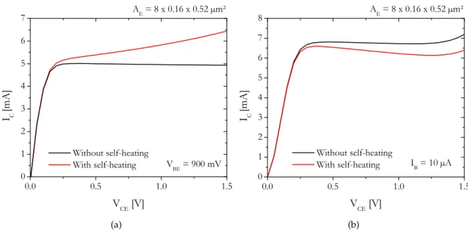
In SiGe HBTs, an increase of the voltage or current bias results in higher power dissipation, and, consequently, to an increase in the device temperature. Moreover, for HBT devices, the collector current features a positive temperature coefficient. Therefore, under a constant VBE
bias, the thermal feedback causes the increase of IC as a function of VCE, as observed in figure
1.10a. On the contrary, the self-heating effect leads to a decrease in ICvalues for a fixed IB bias,
as shown in figure 1.10b. These two curves were obtained using the HiCuM compact model, further described in section 1.5.2, with the self-heating effect activated (red curve) or disabled (black curve).
The device temperature rise, under static operating conditions, is calculated according to equa-tion (1.6) [32].
∆T=Tj−Tamb= PdissRTH (1.6)
where Tj is the junction temperature, Tamb is the ambient temperature, RTHis the thermal
0.0 0.5 1.0 1.5 0 1 2 3 4 5 6 7 V BE = 900 mV V CE [V] I C [ m A ] Without self-heating With self-heating A E = 8 x 0.16 x 0.52 µm² (a) 0.0 0.5 1.0 1.5 0 1 2 3 4 5 6 7 8 A E = 8 x 0.16 x 0.52 µm² Without self-heating With self-heating I C [ m A ] V CE [V] I B = 10 µA (b)
Figure 1.10: Output characteristics under (a) a constant VBE bias and (b) a constant IB bias with and
without self-heating effect.
Base push-out
The base push-out or Kirk effect [33] leads to an increase of the forward transit time, and con-sequently, to a drop in the transit frequency at high current densities, as illustrated in figure 1.11. 10 -5 10 -4 10 -3 10 -2 10 -1 0 50 100 150 200 250 300 A E = 8 x 0.16 x 0.52 µm² C u t -o f f f r e q u e n c y [ G H z ] I C [A] V CB = 0 V
Kirk effect onset
Figure 1.11: Evolution of the transit frequency according to the collector current depicting the Kirk effect onset at high current densities.
This effect occurs when the mobile charge in the BC-SCR becomes greater than the fixed ionized charge which leads to the spreading of the neutral base region towards the collector at high current densities [21]. The critical current for the Kirk effect onset is given by,
1.4. Device operation 17
where AEis the emitter area, Ndcis the collector doping level and vsatis the saturation velocity
of electrons. To enhance the dynamic performances of SiGe HBTs, the Kirk effect must be repel to higher current densities requesting an increased collector doping which causes a significant degradation of the breakdown voltages.
Quasi-saturation
The quasi-saturation effect occurs at high-injections due to the internal collector resistance [21] of the transistor. An increased of the collector current leads to a large voltage drop across the collector resistance, which, thereby, causes the forward biasing of the BC junction. On the forward Gummel plot from figure 1.12a, a kink on the base current indicates the onset of quasi-saturation. Meanwhile, on the output characteristic from figure 1.12b, the quasi-saturation re-gion is observed at low collector-emitter voltages, where the forward biasing of the BC junction can occur.
(a) (b)
Figure 1.12: (a) Forward Gummel and (b) output characteristic showing the quasi-saturation effect taken from [21].
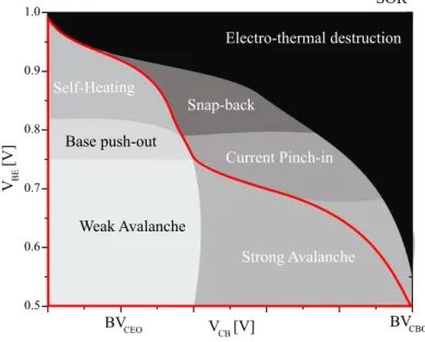
1.4.2 Stable Operation Regime
The surge for higher dynamic performances results in a increasingly restriction of the DC op-erating conditions of SiGe HBTs. For this reason, a stable operation regime (SOR) allows to define the voltage and current ranges for which the transistor operates without catastrophic failure [31]. Depending on the measurement configurations (constant VBE setup, constant IB
steup or constant IE setup), the boundaries of this regime could shift but are still related to the
impact-ionization mechanism [34], as presented in figure 1.13a.
Constant IB setup In the constant IB operation mode, the SOR is mostly limited by the first
breakdown voltage, BVCEO, defined for an open base configuration. For voltages larger than
BVCEO, the avalanche coefficient, M, tends to infinity leading to a sharp increase of the collector
current, IC, as observed on the black curve of figure 1.13a. A biasing beyond the BVCEO will
for a high collector doping concentration, there is a shift of the BVCEOto higher voltages due to
the self-heating and the multiplication factor decrease at high currents [35]. Due to the rare use of the open base configuration in circuit designs, this limitation using BVCEOis not relevant.
I E = 0 I B = 0 Constant I B setup Constant I E setup Constant V BE setup Snapback V CE I C BV CBO + V BE BV CEO 0 Pinch-in effect (a) 0.0 0.5 1.0 1.5 2.0 2.5 3.0 3.5 4.0 10 -4 10 -3 10 -2 10 -1 V CE [V] I C [ A ] Second snapback First snapback V BE = 800mV 300 400 500 600 700 800 D e v i c e t e m p e r a t u r e [ K ] (b)
Figure 1.13: (a) Influence of the measurements configurations on a HBT output characteristic and (b) Device junction temperature for a constant VBEsetup.
Constant IEsetup The constant IE setup configuration is more frequently used, especially in
high-speed circuits with amplifier stages. This operation mode is first limited by the second breakdown voltage, BVCBO, at low current densities due to an infinite avalanche current that
causes the transistor catastrophic failure. At moderate emitter current densities, the pinch-in effect occurs as reported on the blue curve of figure 1.13a. This mechanism translates an abrupt pinch of the emitter current at the emitter center resulting in an instability of the collector current [36].
Constant VBE setup Finally, in the constant VBE operation mode, the output voltage is
re-stricted by (i) the BVCBO at low VBE, (ii) the pinch-in effect at moderate VBE and (iii) the
snap-back mechanism at high VBE. The first two limitations are shared with the IE setup
configu-ration while the last one, the snap-back mechanism, only occurs in this particular opeconfigu-ration mode. This effect is depicted on the orange curve of figure 1.13a where three collector cur-rent values can be obtained for a given VBE/VCE resulting in electrical instabilities. In [37],
the snap-back mechanism is associated to the voltage drop across the series resistances at high current densities. Moreover, since this mechanism is related to the avalanche and self-heating effects [37], the device temperature is also depicted in figure 1.13b together with the collector current behavior. One observes that the snap-back mechanism leads to extreme temperatures, up to 300 °C, especially approaching the second fly-back locus. These temperatures can lead to reliability issues such as electro-migration, dopant out-diffusion and, globally speaking, to device performance degradation [37]. Regarding the limitations previously defined, the cor-responding stable operating regime for constant VBE measurement condition is illustrated in
1.5. Compact modeling 19 0.5 0.6 0.7 0.8 0.9 1.0 BVCBO VBE [V] VCB [V] BVCEO Electro-thermal destruction Self-Heating Current Pinch-in Strong Avalanche Weak Avalanche SOR Snap-back Base push-out
Figure 1.14: Stable Operation Regime for a constant VBEsetup on a high-speed SiGe HBT.
1.5
Compact modeling
1.5.1 History
A compact model is an equivalent circuit composed of discrete elements (diodes, capacitors, resistors) that are connected to each other. Each element is described by a set of analytical equations that model the device characteristics of the component based on its electrical behav-ior. Compared to 2D/3D numerical device simulators (such as TCAD), compact models offer an attractive trade-off between the computational efficiency and the results accuracy compared to measurements. Compact models are embedded inside a simulation framework, such as ADS, ELDO or HSPICE, providing a reliable and accurate tool for the simulation of integrated circuits.
Regarding bipolar transistors, the first compact model was published in 1954 by Ebers and Moll [38] describing the static operation of the device in forward and reverse active regime. In 1975, the SPICE Gummel-Poon (SGP) [39] was developed at the University of Berkeley and is a simplified formulation of the work of Gummel and Poon [40]. The latter were the first to introduce the generalized integral charge-control relation (GICCR) into the bipolar transistor model. Originally developed for the design of high-speed integrated circuits, the High Current Model (HiCuM) [41], [42] has emerged in 1986. Based on the GICCR, this compact model provides an accurate modeling of the transit time in all transistor operating regimes. Therefore, it has become one of the most widely used compact models in the semiconductor industry. A quick overview of this model is proposed in the next section. In a similar effort to improve the SGP model, two other compact models were introduced in the 90’s: The Most Exquisit Transistor Model (MEXTRAM) by Philips [43] and the Vertical Bipolar Inter-Company (VBIC) model by Motorola [44]. Both of them are based on the Kull model [45] for the modeling of
![Figure 1.3: Potential applications for silicon integrated mm-wave and THz circuits taken from [5].](https://thumb-eu.123doks.com/thumbv2/123doknet/14551738.725739/29.892.251.647.124.543/figure-potential-applications-silicon-integrated-wave-circuits-taken.webp)
![Figure 1.5: Schematic cross-section of a high-speed SiGe HBT taken from [5].](https://thumb-eu.123doks.com/thumbv2/123doknet/14551738.725739/32.892.161.709.247.547/figure-schematic-cross-section-high-speed-sige-taken.webp)
![Figure 1.6: Schematic flow of the selective epitaxial growth of the base link region in both DSPA (left) and EBL (right) processes taken from [22].](https://thumb-eu.123doks.com/thumbv2/123doknet/14551738.725739/33.892.200.699.134.353/figure-schematic-selective-epitaxial-growth-region-dspa-processes.webp)
![Figure 1.7: Schematic cross section of an NSEG HBT with elevated extrinsic base (EEB) regions taken from [5].](https://thumb-eu.123doks.com/thumbv2/123doknet/14551738.725739/34.892.268.632.198.461/figure-schematic-cross-section-nseg-elevated-extrinsic-regions.webp)

![Figure 1.21: TEM cross-section of a 0.1 x 4.9 µm 2 HS SiGe HBT from B55 technology [23].](https://thumb-eu.123doks.com/thumbv2/123doknet/14551738.725739/46.892.289.606.694.1007/figure-tem-cross-section-µm-sige-hbt-technology.webp)