HAL Id: hal-02403172
https://hal.archives-ouvertes.fr/hal-02403172
Submitted on 14 Dec 2020
HAL is a multi-disciplinary open access
archive for the deposit and dissemination of
sci-entific research documents, whether they are
pub-lished or not. The documents may come from
L’archive ouverte pluridisciplinaire HAL, est
destinée au dépôt et à la diffusion de documents
scientifiques de niveau recherche, publiés ou non,
émanant des établissements d’enseignement et de
Ti segregation at CoSi grain boundaries
Hannes Zschiesche, Ahmed Charai, Dominique Mangelinck, Claude Alfonso
To cite this version:
Hannes Zschiesche, Ahmed Charai, Dominique Mangelinck, Claude Alfonso.
Ti
segrega-tion at CoSi grain boundaries.
Microelectronic Engineering, Elsevier, 2019, 203-204, pp.1-5.
�10.1016/j.mee.2018.10.009�. �hal-02403172�
Ti excess at CoSi
2grain boundaries
H. Zschieschea,∗, A. Chara¨ıa, D. Mangelincka, C. Alfonsoa
aAix-Marseille Universit´e, IM2NP, CNRS, Facult´e de Saint-J´erˆome, Case 142, 13397
Marseille Cedex 20, France
Abstract
The localization of Ti at grain boundaries after the phase formation of CoSi2
on Si(111) from a Co-Ti bilayer is examined. For the chemical analysis at the atomic scale, atom probe tomography (APT) is applied. The structure of grain boundaries is analyzed by high resolution transmission electron microscopy (HR TEM). A polycrystalline CoSi2 film has been formed after annealing. Inside
the grains of CoSi2, Ti is determined to be present in low concentration of
0.2 at %. An excess of Ti is measured at the grain boundaries. The Ti excess varies for different grain boundaries. HR TEM shows different distances between defects for varying misorientation. The distances between defects are compared with theoretical misfits at the grain boundaries. A relationship between the Ti excess at grain boundaries determined by APT and the defect densities of grain boundaries analyzed by HRTEM is proposed.
Keywords: Cobalt disilicide, Ti excess at CoSi2 grain boundary, Atom probe
tomography, Transmission electron microscopy
1. Introduction
CoSi2films on Si substrates are widely used in microelectronic applications
as contact material beside TiSi2 and NiSi films, depending on the scale. Low
electrical resistivity, high thermal stability and the good match of the crystal structure with Si are the main advantages of CoSi2 [1]. The aim of the intro-5
∗Corresponding author: Hannes Zschiesche
duction of a Ti interlayer between the Co film and the Si substrate was to grow CoSi2 as a single crystal in epitaxy on Si(100) or Si(111) by sputtering
deposi-tion and reactive diffusion [2].
The role of the Ti interlayer during the phase formation has been investigated and explanations were proposed. Two possibilities are considered: a) the
re-10
duction of native oxide on the silicon substrate b) the formation of a Ti rich phase acting as a diffusion or reaction barrier. Both possibilities should provide homogeneous diffusion and phase formation. The influence of parameters such as the deposition of an alloy instead of a bilayer [3], the substrate orientations [4], annealing environments [5], annealing temperatures [6], thickness of the Ti
15
interlayer or the Co layer [7] or other elements for the interlayer [8] have been investigated to get a better understanding and a better process. The influence of a Ti capping layer instead of a Ti interlayer was also reported [9, 10]. The Ti capping layer induced an increase of the nucleation temperature of CoSi2 as
well as a preferred texture in comparison to the growth without capping Ti.
20
These effects can be explained by the diffusion of Ti from the capping layer to the interface.
As Ti is only slightly soluble in CoSi2, it was assumed that Ti has to be present
in the grain boundaries (GBs) after the formation of CoSi2. However, to the
best knowledge of the authors, the presence of Ti at the GBs after the formation
25
of CoSi2 has not been shown yet.
Atom probe tomography (APT) enables to detect single atoms and to recon-struct them in 3D volumes with atomic resolution. It allows to quantify tiny excess (number of atoms per unit area [11]) of elements at 2D structures such as GBs or interfaces [12]. An excess of elements can origin from strain fields
30
induced by defects [13] as they are present on GBs. The combination of APT and transmission electron microscopy (TEM) is a powerful method to compare excess of elements with structural defects [14].
The aim of this work is the chemical investigation of CoSi2 GBs by APT. The
structure at different GBs is analyzed by TEM. A comparison of the
deter-35
transmission electron microscopy (HRTEM) investigations will be discussed.
2. Materials and Methods
Si(111) wafers have been immersed in a 5 % dilute HF for 1 min to remove native oxide before load in the sputtering system. Successive deposition of 5 nm
40
Ti and 100 nm Co from two individual targets of Ti and Co (both 99.99 % pu-rity) has been done by magnetron sputtering. The deposition was performed with a base pressure of about 10−8 Torr using 99.9999 % pure Ar gas flow of 6.7 sccm at room temperature. Thermal annealing were performed in vacuum up to 850◦C to fully transform the as-deposited bilayer film into CoSi2. 45
X-ray diffraction (XRD) measurements (here not shown) performed in the Bragg-Brentano geometry, with a 1.5◦ offset to avoid the signal from the substrate, show the presence of CoSi2 with a strong peak of the (111) orientation and
minor peaks of further orientations. TEM lamellas and APT tips have been prepared using a focused ion beam (FIB) FEI Helios 600. APT measurements
50
were performed on a LEAP 3000 HXR. Voltage mode at 40 K, 200 kHz, 20 % pulse fraction and 0.2 % detection rate was applied in order to get optimal information in the compromise of resolution and volume size. IVAS software was used for the reconstruction following the common procedure [15, 16]. TEM has been performed on a TECNA¨I G20 for microstructure investigations and
55
energy dispersive X-ray spectroscopy (EDS) analysis and on a Cs-corrected
TI-TAN 80-300 equipped with a GIF Tridiem 863. The acceleration voltage was always chosen to be 200 kV.
3. Results
3.1. APT
60
Figure 1 presents three APT volumes which contain each one GB. The pres-ence of the GB is indicated by an increased Ti concentration along a flat plane, as highlighted in figure 1 by the isoconcentration surface for Ti 1.5 at %. In order to determine the amount of Ti at the GBs, cylinders with a diameter of
Figure 1: APT volumes of CoSi2 contain GBs with excess of Ti (1.5 at. % isosurface
25 nm have been placed with their z-axis along the normal of the GB plane as
65
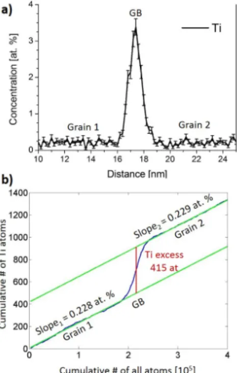
shown in figure 1. The 1d concentration profile has been measured along the z-axis of these cylinders as shown in figure 2a for the cylinder in figure 1a. A low constant concentration can be seen inside the grains. At the GB, a sharp peak of Ti indicates the increased concentration of Ti. The full width at half maximum (FWHM) of the peak is about 1.5 nm.
Figure 2: a) The concentration profile along the z-axis of the cylinder in figure 1a visualizes the increased concentration of Ti at the GB. b) The constant concentration inside the grains can be fitted with a linear function in the integral profile. The slope corresponds to the concentration (about 0.2 at. % for both grains). The step height at the GB is related to the number of Ti atoms on the base area of the cylinder (415 at).
70
However, the comparison of the excess concentration at a GB is only semi-quantitative. The spatial resolution in the APT is not isotropic and thus ex-perimental broadening due to different spatial resolution can occur depending on the orientation of the grain boundary inside the APT tip volume. This can
change the local excess concentration of identical grain boundaries. In contrast,
75
the determination of the excess number of atoms projected on the GB plane allows a more quantitative comparison as it is not affected by anisotropic effects [11]. The value of the Ti excess at the GB can be specified as the number of atoms per unit area. Thus, experimental broadening of the GB plane has no influence on the excess quantity.
80
The accumulation of Ti atoms over the accumulation of all atoms along the z-axis of the cylinder is shown in the integral profile (Figure 2b). For a constant concentration, as seen in the grains, a linear behavior is verified: the concentra-tion is determined from the slope of the fit. The Ti concentraconcentra-tion in the grains is about 0.2 at %. The offset between the two slopes of the grains at the GB
85
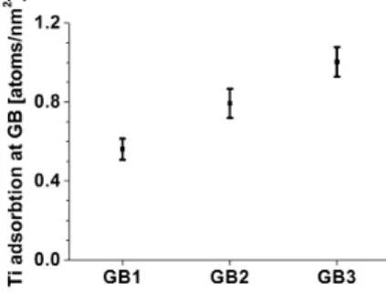
corresponds to the Ti excess at the analyzed GB area (red line). In this exam-ple it is determined to 415 atoms integrated over the base area of the cylinder. Dividing the number of atoms by the base area of the cylinder gives the value of Ti excess at the GB per unit area. The same procedure was applied for the three different GBs from figure 1 and the Ti excess is visualized in figure 3. The
90
Ti excess is significantly different for the three investigated GBs.
Figure 3: The comparison of Ti excess at different GBs shows a significant variation.
3.2. TEM
Figure 4 shows a low angle tilt GB. The fast Fourier transformations (FFT) (inset in figure 4a) demonstrates that both adjacent grains are in [10-1] zone
Figure 4: HREM on low angle tilt GB. a) Two grains in [10-1] zone axis are slightly tilted around the [10-1] axis to each other (about 5◦). b) Bragg filtering of (1-11) planes visualizes
the misorientation of the grains. Furthermore, defects along the GB becomes visible.
axis and thus have a close relationship. A rotation of about 5◦ around the
[10-95
1] axis can be measured in the FFT of a region including both grains, where two spots are found close to each other for all directions (inset figure 4b). A rotation axis parallel to GB plane, as in this example, identifies a tilt GB. Different intensities of spots for same directions of the both grains indicate that an additional misorientation is present. However, due to the fact that both
100
grains are in the same zone axis, the total misorientation is assumed to be low and the GB has a main low angle tilt character.
Figure 4b is an image obtained only from the (1-11) spots of the FFT. It shows the (1-11) planes of CoSi2. This Bragg-filtered image of selected planes,
Figure 5: HREM on special GB. a) Two grains in [111] and [010] zone axis are visible. The misorientation of the two zones is 54.7◦. Both grains have the (¯202) planes in common. b) Bragg filtering of the (¯202) planes shows defects at the GB in very large distance (about 11.6 nm) compared to figure 4.
visualizes defects along the GB. They show a periodic distance of about 3.5 nm.
105
Figure 5 is an example for a special twist GB [17]. The two adjacent grains are in different low indexed zone axis ([111] and [010], compare FFTs of insets in figure 5). They have the (¯202) planes in common. Thus, the rotation axis is perpendicular to the (¯202) planes. Furthermore, the GB plane is aligned close to the (¯202) planes and so the rotation axis is almost perpendicular to the GB
110
plane. That identifies a main twist GB character. The misorientation of the two zone axis is 54.7◦. Figure 5b is the Bragg-filtered image of the (¯202) planes.
Defects in the (¯202) planes can be found and are highlighted. The distance is about 11.6 nm. Their origin is in the mismatch of the planes perpendicular to the GB plane. In parallel to the viewing direction these are the (¯24¯2) planes for
115
the grain on the left side of the figure and the (20¯2) planes for the grain on the right side of the figure (normal vectors of planes indicated in figure 5b). EDS, energy-filtered transmission electron microscopy (EFTEM) and scanning transmission electron microscopy (STEM) electron energy loss spectroscopy (EELS) have been applied in order to investigate the presence of Ti at the
120
GBs directly in TEM (not shown). However, no Ti excess was detected at dif-ferent GBs. Since the APT results of section 3.1 show a systematic enrichment of Ti on GBs, the local concentration variation of Ti should be under the de-tection limit of these analytical TEM techniques and the combination of TEM and APT is crucial for this investigation.
125
4. Discussion
The values of Ti excess at CoSi2GBs investigated by APT determine a
num-ber of atoms per unit area. In the Gibbs approach, it is assumed that all the excess atoms are located on the GB plane with no thickness. The sharp peak at the GB in the concentration profile of figure 2a justifies that assumption.
130
The FWHM is about 1.5 nm and can be explained by experimental broadening. Furthermore, the defects in the GB plane can be energetically favorable posi-tions for Ti atoms, as seen for other material system with excess on defects [13]. Thus, it is of interest to estimate a defect density per unit area on the GBs from the TEM investigations and compare them with the Ti excess.
135
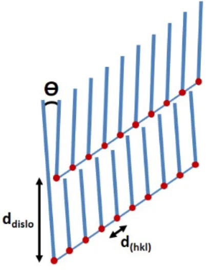
Figure 4 shows that the distance between the defects along a low angle GB plane is about ddislo= 3.5 nm. Low angle tilt GBs are well described by edge
dislocations parallel to the rotation axis [18]. Their distance ddislois geometrical
predicted from the Read and Shockley expression ddislo = b/Θ where b is the
norm of the Burgers vector and Θ is the misorientation of the GB [19]. With
140
Figure 6: Schematic drawing of defect density calculation on low angle tilt GB with edge dislocations paralle to the rotation axis.
of the GB by HRTEM, the norm of the Burgers vector can be calculated to b = 0.31 nm, even if the quality of the HRTEM image is not sufficient for a direct determination. This value is in the order of the lattice plane distances of CoSi2 (1¯11) planes. Thus, it can be assumed that there are primary ~b=a(1¯11) 145
edge dislocations at the [10¯1] low angle tilt GB. For verification it is necessary to determine the orientation of the Burgers vector in a HRTEM image. Modeling the low angle tilt GB by the superposition of supercells in [10¯1] orientation and 5◦ misorientation verifies a distance of atomic positions in coincidence of about 3.5 nm.
150
Additional planes from edge dislocations are normal to the plane of the HRTEM image. Their distance is identical to the atomic spacing between the lattice planes in the viewing direction [10¯1] (d(10¯1) = 0.378 nm). From that, the unit
area for one defect is calculated to d(10¯1)×ddislo= 1.33 nm2(compare scheme in
figure 6). If every defect core is occupied by one Ti atom, an Ti excess of about
155
0.75 atoms/nm2 is expected for the investigated low angle GB. This estimation
of the excess value is in between the two Ti excesses determined by APT at the GB1 and GB2 (Figure 3).
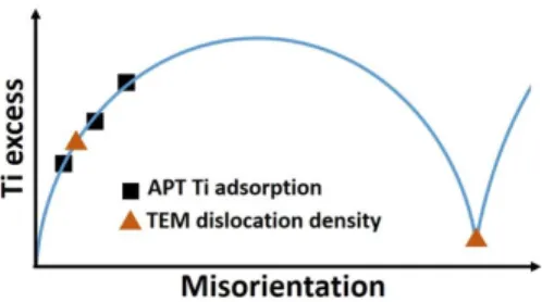
Figure 7: Schematic drawing of Ti excess over misorientation compared with estimated GB defect density.
In figure 7, a schematic model of the relation between the Ti excess at the GB and their misorientation is drawn. As it is assumed that the Ti excess is
160
correlated to the defect density, it is expected to be minimal for very low mis-orientation and at special GBs where the lattices of both adjacent grains are in high coincidence. From the calculation above, the Ti excess of GB1 and GB2 investigated by APT are slightly smaller and bigger than the defect density at the low angle GB investigated in TEM. It can be estimated that they are in the
165
same misorientation region, as well as GB3.
The defects in the special GB (Figure 5) have a distance 3 times larger than the defects in the presented low angle GB. Thus, a significant lower defect density and by this Ti excess at the GB would be expected to be measured.
The measured defect distance can be verified by comparison of the distance
be-170
tween coincidence sites of the different planes parallel to the viewing direction perpendicular to the GB. Their normal vectors are drawn in figure 5b. For the grain on the left in [111] viewing direction it corresponds to the atomic spacing between (¯24¯2) planes d(¯24¯2) = 2.187 nm. For the grain on the right in [010]
viewing direction it corresponds to the atomic spacing between (20¯2) planes
175
d(20¯2)= 1.894 nm. Distances between defects along the GB are estimated to be at minimums of the differences in multiple atomic distances which are coinci-dent sites for differences close to 0. After 7 and 6 atomic distances, respectively, the difference has a minimum. Thus, the distance of defects is estimated to be about 13.2 nm, that is in the order of the measured distance. The (¯24¯2) planes
are not resolved, thus a simultaneous Bragg-filtering of (¯24¯2) and (202) planes is not possible.
However, strong assumptions have been made to calculate the defect density on the GB plane from HRTEM image. The number of Ti atoms localized per defect might be also different from one. In addition, different kinds of defects
185
(edge, screw or mixed dislocations, steps...) may have different behavior in view on Ti excess. Simulations could help to compare the proposed relationship to theoretical thermodynamic results.
To improve the interpretation of the presented results, a precise correlation of the Ti excess to the GB misorientation and the GB plane would be necessary.
190
In principal, acquired APT volumes can contain enough crystallographic infor-mation to determine the misorientation through the density variation along the crystallographic poles and lattice planes [20, 21]. Nevertheless, obtaining this information is difficult and usually works easier for pure metals [20, 21]. More-over, there are limitations if the GB is at the border of the APT volume. In the
195
volumes shown in figure 3b and 3c, there is not enough information to determine the misorientation properly. Another method to determine the misorientation of the GB is the use of electron microscopy before the APT run. Indeed, ori-entation mapping of the tip by transmission Kikuchi diffraction (TKD) in a scanning electron microscope (SEM) or by nanobeam diffraction in a TEM has
200
shown to be promising for systematic investigations between misorientation and excess at GBs [22, 23].
Further studies are in progress to get better correlation between the misorien-tation and the Ti excess as well as correlation between the structure of CoSi2
GBs and the Ti excess.
205
5. Conclusion
In conclusion, Ti segregates to grain boundaries of CoSi2. The amount of
excess depends on the grain boundary characteristic as misorientation and defect structure. A relationship between defects and Ti localization is proposed. It
could be verified by a correlated study of HRTEM and APT on identical GBs
210
as well as by an exhaustive study of correlation between misorientation and Ti excess.
Acknowledgment
This work was supported by the French government through the program ”Investissements d’Avenir A*MIDEX” (Project APODISE, no.
ANR-11-IDEX-215
0001-02) managed by the National Agency for Research (ANR). The authors would like to thank M. Bertoglio for assistance with sample growth, M. Descoins for assistance with APT and T. Neisius, A. Campos, M. Cabie, L. Patout and C. Dominici for assistance with TEM and fruitful discussions.
References
220
[1] S. P. Murarka, Intermetallics 3 (1995) 173–186. doi:10.1016/ 0966-9795(95)98929-3.
[2] M. L. A. Dass, D. B. Fraser, C.-S. Wei, Appl.\ Phys.\ Lett. 58 (1991) 1308. doi:10.1063/1.104345.
[3] S. L. Hsia, T. Y. Tan, P. Smith, G. E. McGuire, J. Appl. Phys. 70 (1991)
225
7579–7587. doi:10.1063/1.349713.
[4] P. Liu, B. Z. Li, Z. Sun, Z. G. Gu, W. N. Huang, Z. Y. Zhou, R. S. Ni, C. L. Lin, S. C. Zou, F. Hong, G. A. Rozgonyi, J. Appl. Phys. 74 (1993) 1700–1706. doi:10.1063/1.354824.
[5] T. I. Selinder, T. A. Roberts, D. J. Miller, M. A. Beno, G. S. Knapp,
230
K. E. Gray, S. Ogawa, J. A. Fair, D. B. Fraser, J. Appl. Phys. 77 (1995) 6730. URL: http://ieeexplore.ieee.org/articleDetails.jsp? arnumber=5151061. doi:10.1063/1.359091.
[6] F. Hong, G. A. Rozgonyi, B. K. Patnaik, Appl. Phys. Lett. 64 (1994) 2241– 2243. URL: http://aip.scitation.org/doi/10.1063/1.111657. doi:10.
235
1063/1.111657.
[7] A. Vantomme, M. A. Nicolet, N. D. Theodore, J. Appl. Phys. 75 (1994) 3882–3891. doi:10.1063/1.356033.
[8] C. Detavernier, R. L. Van Meirhaeghe, F. Cardon, K. Maex, H. Bender, B. Brijs, W. Vandervorst, J. Appl. Phys. 89 (2001) 2146–2150. doi:10.
240
1063/1.1340598.
[9] C. Detavernier, R. L. Van Meirhaeghe, F. Cardon, R. A. Donaton, K. Maex, Microelectron. Eng. 50 (2000) 125–132. doi:10.1016/S0167-9317(99) 00272-5.
[10] C. Detavernier, R. L. Van Meirhaeghe, W. Vandervorst, K. Maex,
Micro-245
electron. Eng. 71 (2004) 252–261. doi:10.1016/j.mee.2003.12.002. [11] B. W. Krakauer, D. N. Seidman, Phys. Rev. B 48 (1993) 6724–6727. doi:10.
1103/PhysRevB.48.6724.
[12] M. A. Khan, S. P. Ringer, R. Zheng, Adv. Mater. Interfaces 3 (2016). doi:10.1002/admi.201500713.
250
[13] A. Kwiatkowski da Silva, G. Leyson, M. Kuzmina, D. Ponge, M. Herbig, S. Sandl¨obes, B. Gault, J. Neugebauer, D. Raabe, Acta Mater. 124 (2017) 305–315. doi:10.1016/j.actamat.2016.11.013.
[14] A. Stoffers, J. Barthel, C. H. Liebscher, B. Gault, O. Cojocaru-Mir´edin, C. Scheu, D. Raabe, Microsc. Microanal. 23 (2017) 291–299. doi:10.1017/
255
S1431927617000034.
[15] P. Bas, A. Bostel, B. Deconihout, D. Blavette, Appl. Surf. Sci. 87-88 (1995) 298–304. doi:10.1016/0169-4332(94)00561-3.
[16] F. Vurpillot, B. Gault, B. P. Geiser, D. J. Larson, Ultramicroscopy 132 (2013) 19–30. doi:10.1016/j.ultramic.2013.03.010.
[17] V. Randle, Scr. Mater. 54 (2006) 1011–1015. doi:10.1016/j.scriptamat. 2005.11.050.
[18] L. Prieseter, Grain boundaries from theory to engineering, 2012. doi:10. 1007/978-3-642-33848-9.
[19] W. T. Read, W. Shockley, Phys. Rev. 78 (1950) 275–289. URL: https:
265
//link.aps.org/doi/10.1103/PhysRev.78.275. doi:10.1103/PhysRev. 78.275.
[20] M. P. Moody, F. Tang, B. Gault, S. P. Ringer, J. M. Cairney, Ultra-microscopy 111 (2011) 493–499. URL: http://dx.doi.org/10.1016/j. ultramic.2010.11.014. doi:10.1016/j.ultramic.2010.11.014.
270
[21] L. Yao, M. P. Moody, J. M. Cairney, D. Haley, A. V. Ceguerra, C. Zhu, S. P. Ringer, Ultramicroscopy 111 (2011) 458–463. URL: http://dx.doi.org/ 10.1016/j.ultramic.2010.11.018. doi:10.1016/j.ultramic.2010.11. 018.
[22] K. Babinsky, W. Knabl, A. Lorich, R. De Kloe, H. Clemens, S. Primig,
275
Ultramicroscopy 159 (2015) 445–451. URL: http://dx.doi.org/10.1016/ j.ultramic.2015.05.014. doi:10.1016/j.ultramic.2015.05.014. [23] M. Herbig, D. Raabe, Y. J. Li, P. Choi, S. Zaefferer, S. Goto, Phys. Rev.

![Figure 4: HREM on low angle tilt GB. a) Two grains in [10-1] zone axis are slightly tilted around the [10-1] axis to each other (about 5 ◦ )](https://thumb-eu.123doks.com/thumbv2/123doknet/14640928.735274/8.918.338.571.184.631/figure-hrem-angle-tilt-grains-zone-slightly-tilted.webp)
![Figure 5: HREM on special GB. a) Two grains in [111] and [010] zone axis are visible. The misorientation of the two zones is 54.7 ◦](https://thumb-eu.123doks.com/thumbv2/123doknet/14640928.735274/9.918.364.555.183.669/figure-hrem-special-grains-zone-visible-misorientation-zones.webp)