HAL Id: hal-01779321
https://hal.archives-ouvertes.fr/hal-01779321
Submitted on 26 Apr 2018
HAL is a multi-disciplinary open access
archive for the deposit and dissemination of
sci-entific research documents, whether they are
pub-lished or not. The documents may come from
teaching and research institutions in France or
abroad, or from public or private research centers.
L’archive ouverte pluridisciplinaire HAL, est
destinée au dépôt et à la diffusion de documents
scientifiques de niveau recherche, publiés ou non,
émanant des établissements d’enseignement et de
recherche français ou étrangers, des laboratoires
publics ou privés.
Self-consistent physical modeling of set/reset operations
in unipolar resistive-switching memories
Marc Bocquet, Damien Deleruyelle, Christophe Muller, Jean-Michel Portal
To cite this version:
Marc Bocquet, Damien Deleruyelle, Christophe Muller, Jean-Michel Portal. Self-consistent physical
modeling of set/reset operations in unipolar resistive-switching memories. Applied Physics Letters,
American Institute of Physics, 2011, 98 (26), �10.1063/1.3605591�. �hal-01779321�
resistive-switching memories
Marc Bocquet,1, a)Damien Deleruyelle,1 Christophe Muller,1and Jean-Michel Portal1
IM2NP, UMR CNRS 6242, Aix-Marseille Universit´e, 38 rue Joliot Curie, 13451 Marseille Cedex 20, France
(Dated: 4 May 2012)
This letter deals with a self-consistent physical model for set /reset operations involved in unipolar resistive switching memories integrating a transition metal oxide. In this model, set operation is described in terms of a local electrochemical reduction of the oxide leading to the formation of metallic conductive filaments. Beside, reset operation relies on the thermally-assisted destruction of the formed metallic filaments by Joule heating effect. An excellent agreement is demonstrated with numerous published experimental data suggesting that this model can be confidently implemented into circuit simulators for design purpose.
Memory devices based on resistive switching materi-als are currently pointed out as promising candidates to replace conventional non-volatile memory devices based
on charge-storage beyond 2x nm-technological nodes.1
In particular, devices integrating a transition metal
oxide (so-called TMO) such as NiO, TiO2, ZnO or
CuxO, are of growing interest due to their simple
Metal/Insulator/Metal (MIM) structure, oxides com-patible with complementary metal-oxide-semiconductor
technology and low process temperature.2 So far, in
TMO-based memory devices, the unipolar switching be-tween low resistance state (LRS) and high resistance state (HRS) is explained in terms of creation/destruction
of conductive filaments within the oxide.3,4 Waser et al.5
explained that set, i.e. the transition from HRS to LRS, originates from a local reduction reaction leading to the creation of metallic conductive filaments (CF). During reset, local dissipation of Joule power enhances the ther-mally activated diffusion of defects and/or of different atomic species constituting the CF combined with a local
oxidation process.6,7Based on this phenomenological
de-scription, several models for reset were reported in Refs.
8–10 but very few offer a model for set.11 Furthermore,
it has to be stressed that there is currently no complete model taking into account both set and reset operations that could be easily implemented in circuit simulators for design purpose.
In this context, this paper proposes a self-consistent physical model accounting for both set /reset operations in NiO-based unipolar resistive switching devices. Af-ter uncovering the theoretical background and the set of relevant physical parameters, the model is confronted to quasi-static and dynamic experimental data from litera-ture.
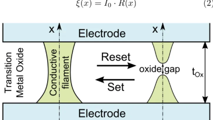
Fig. 1 schematically describes the set /reset mecha-nisms controlling the resistive switching phenomenon. Set (resp. reset ) is assumed to be due to the creation (resp. destruction) of CF between two electrochemically inert electrodes. Starting from LRS, the existing CF may
a)Electronic mail: [email protected]
be heated by Joule effect thanks to the application of an electric field ξ, as reported in Ref. 12. CF top and bot-tom boundaries are kept at thermal equilibrium with
con-nected electrodes at room temperature (Tamb) whereas
the sidewalls are expected to exchange heat flow with the surrounding oxide. Thus, in one dimension geometry the heat equation can be simply written as:
σCF(x) · ξ(x)2= −KthCF ∂2TCF(x) ∂x2 + h TCF(x) − TOx tOx (1)
where σCF is the CF conductivity, TCF(x) the CF
tem-perature, TOxthe oxide temperature, KthCF the CF
ther-mal conductivity, tOx the oxide thickness and h the heat
transfer coefficient between CF and surrounding oxide. In LRS CF is assumed to be metallic with a high
con-ductivity σCF. In contrast, when CF is dissolved, the
resistance of MIM structure is controlled by the resulting oxide gap separating the two CF fragments (cf. Fig. 1).
As a consequence, a lower conductivity noted σOx
ac-counts for the electronic transport in HRS. Assuming the current conservation through the whole structure, an an-alytical expression of the electric field ξ can be derived (∇J = 0): ξ(x) = I0· R(x) (2)
Electrode
Electrode
Tr ansi tion M etal Oxid e Co nd uctive fila m en tReset
Set
x
x
oxide gapt
OxFIG. 1. Schematic representation of a formed and dissolved conductive filament resulting from set and reset operations respectively in MIM structure. During reset, the inner tem-perature is raised by Joule effect and leads to the destruction of the CF. In contrast, during set a electrochemical local re-duction process enables restoring CF.
2 where the resistance per unit length R(x) is
R(x) = 1 r2 CF(x)π(σCF(x) − σOx) + r2CFmaxπσOx (3) I0= VCell RtOx 0 R(x)dx (4)
I0 is the ohmic current in the MIM structure, VCell the
applied voltage, rCF(x) and rCFmax denote respectively
the radius and the maximal radius of the CF in cylindri-cal geometry.
Two distinct mechanisms were considered to describe the creation and the destruction of CF: a local redox
process5,13 and a thermally-assisted diffusion8. One can
consider a classical redox equations such as:
Ni2++ 2 · e−
ox
red
Ni (5)
in which the reaction velocities for both reduction and oxidation processes may be expressed classically by the
Butler-Volmer equation:14 νred= k0e −∆rG0+ 2(1 − α)F (E − Eeq) R · Tox (1−CN i) (6) νox= k0e −∆rG0− 2αF (E − Eeq) R · TCF(x) CN i (7)
α is the asymmetry factor, k0 kinetics constant of
elec-trochemical reaction, R is the ideal gas constant, F is the
Faraday constant, ∆rG0is the free energy of the reaction
at equilibrium and finally Eeq is the equilibrium
poten-tial. Moreover CN idenotes the dimensionless
concentra-tion of metallic species. To determine the potential of the
reduced and oxidized species such as Ni and Ni2+
respec-tively, the mechanism is supposed to be isotropic and the
redox potential E is assumed to be equal to −|VCell|.
Finally, in order to properly account for the metallic nature of the CF, its conductivity relies on a temperature
coefficient αT as described by Russo et al.12 where σCF0
is the CF conductivity at room temperature (Tamb):
σCF(x) =
σCF0
1 + αT · (TCF(x) − Tamb)
(8)
As already proposed by Russo et al.8, the thermal
rup-ture of CF in reset operation can be described by a local
diffusion velocity (νdif f) of the metallic species:
νdif f = kdif f· e
− Ea
kb· TCF(x) · CN i (9)
where Ea is the activation energy governing the
thermally-assisted exodiffusion of metallic species. Regarding Eq.5, we assumed that electron density available during set could not limit the reduction pro-cess. Indeed, during set the growth of the CF is initiated
TABLE I. Physical parameters used for simulations
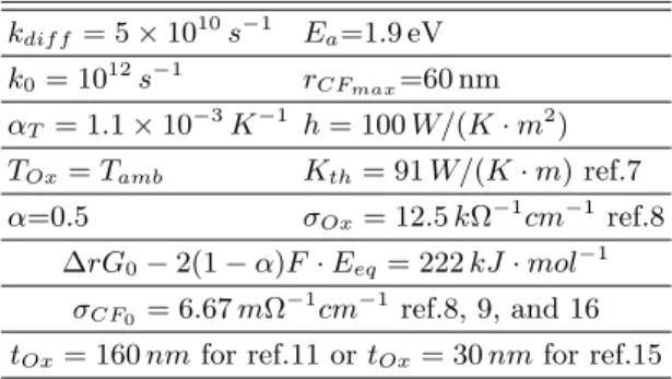
kdif f= 5 × 10¹⁰s−1 Ea=1.9 eV k0= 1012s−1 rCFmax=60 nm αT= 1.1 × 10⁻³K−1 h = 100 W/(K · m2) TOx= Tamb Kth= 91 W/(K · m) ref.7 α=0.5 σOx= 12.5 kΩ−1cm−1ref.8 ∆rG0− 2(1 − α)F · Eeq = 222 kJ · mol−1 σCF0 = 6.67 mΩ −1 cm−1 ref.8, 9, and 16 tOx= 160 nm for ref.11 or tOx= 30 nm for ref.15
at the cathode side. As the CF grows toward the
an-ode, it is assumed to act as ”virtual cathode”5 allowing
electrons to flow freely from the real cathode toward the reduction site.
Finally, the description of set and reset mechanisms enables proposing a self-consistent master equation rely-ing on a chemical kinetics:
dCN i
dt = νred− νox− νdif f (10)
CF radius (rCF = rCFmax×CN i) is calculated from the
electric field (Eq. 2), the CF temperature (Eq. 1), the dif-fusion and reaction velocities (Eqs. 6, 7&9,) and finally from the concentration of metallic species (Eq. 10). It is has to be mentioned that considering energies involved in Eq. 7&9, the CF destruction is mainly governed by the diffusion process rather than oxidation.
To validate the proposed theoritical approach, the model was confronted to quasi-static and dynamic ex-perimental data from the literature. Fig. 2(a) and 2(b) show quasi-static set and reset I(V ) characteristics
mea-0 . mea-0 0 . 5 1 . 0 1 . 5 0 1 x 1 0 - 3 2 x 1 0 - 3 3 x 1 0 - 3 4 x 1 0 - 3 0 . 0 0 . 5 1 . 0 1 . 5 1 0 - 5 1 0 - 4 1 0 - 3 ( a ) I Ce ll ( V ) V C e l l ( V ) IS e t IR e s e t R e f . 1 1 S i m u . t h i s w o r k ( b ) V C e l l ( V ) IS e t IR e s e t R e f . 1 5 S i m u . t h i s w o r k
FIG. 2. Experimental I(V ) characteristics measured on a NiO-based memory structure presented in (a) ref.11 and (b) ref.15 and the corresponding simulation by using the present model and the physical parameters given in Table I. The CF profile obtained after the set operation is used as the initial state to simulate the subsequent reset operation.
sured on NiO-based memory elements by Cagli et al.11
and Lee et al..15 In both studies, memory elements
con-sisted in Pt/NiO/Pt stack with respective nickel oxide
thicknesses of 160 nm11 and 30 nm.15 Using the set of
physical parameters given in Table I together with the actual nickel oxide thickness, the present model shows an excellent agreement with experimental data for both set and reset operations. Moreover, it must be under-lined that the model is used continuously since it relies on a self-consistent kinetics equation accounting for both CF creation and destruction mechanisms. This numer-ical feature is a key point for a model dedicated to an implementation in computer-aided design tools. From a practical point of view, the CF profile obtained after the set operation is used as the initial state to simulate the subsequent reset operation.
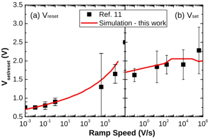
Fig. 3(a&b) shows that the proposed model satisfac-torily matches the experimental increase of set and set voltages along with the programming ramp speed
re-ported by Cagli et al..11The increase of reset voltage may
be interpreted in terms of competition between creation and destruction mechanisms. Indeed, as ramp speed in-creases, a larger current (i.e. a larger applied voltage) is necessary to achieve reset in a shorter time. Through Eq. 6, a larger applied voltage implies a strengthening of the reduction process that limits the filament destruc-tion. Finally, the turn back of the structure toward HRS
is achieved thanks to an increase of Vreset. Beside, the
closing of the gap between Vset and Vreset at highest
sweep rates may lead to some reset /set instabilities as proposed in Ref. 17.
A reported in numerous works, the resistance in
LRS (noted RLRS) and reset current strongly depend
on the maximum current reached during the
preced-ing set operation18–21 (referred as I
SetM ax). This
fea-ture can be understood in terms of reduction of CF ra-dius that concomitantly increases the resistance of the
1 0 - 3 1 0 - 1 1 0 1 1 0 3 1 0 5 0 . 5 1 . 0 1 . 5 2 . 0 2 . 5 3 . 0 3 . 5 1 0 0 1 0 2 1 0 4 1 0 6 ( a ) V r e s e t Vs e t/ re s e t ( V ) R a m p S p e e d ( V / s ) R e f . 1 1 S i m u l a t i o n - t h i s w o r k ( b ) V s e t
FIG. 3. (a) Set and (b) reset voltages as a function of the programming ramp speed based on the experimental results reported in Ref. 11 The calculated curves were obtained for the physical parameters given in Table I.
1 0- 6 1 0- 5 1 0 - 4 1 0- 3 1 0- 2 1 02 1 03 1 04 1 05 1 0- 5 1 0- 4 1 0- 3 1 0- 2 0 . 0 0 . 5 1 . 0 1 . 5 2 . 0 0 3 x 1 0- 3 6 x 1 0- 3 9 x 1 0- 3 1 x 1 0- 2 ( c ) RL R S ( o h m ) I S e t M a x ( A ) R e f . 2 1 R e f . 2 2 R e f . 2 3 R e f . 2 4 R e f . 2 5 S i m u . t h i s w o r k Ire s e t ( A ) ( b ) ICe ll ( A ) S i m u l a t i o n ( a ) V C e l l ( V ) IS e t M a x= 1 0 m A IS e t M a x= 5 m A
FIG. 4. (a) Simulation of set and reset I(V ) characteristics for ISetM ax= 5 mA and 10 mA. (b) Maximum current during the reset operation (IReset) and (c) the resistance in LRS as a function of the maximum current during the preceding set operation (ISetM ax). Experimental data were extracted from Ref. 21–25. The parameters of the Table I were used for simulations.
MIM structure.21
Fig. 4(a) reports the simulated set and reset I(V ) characteristics for two different maximum
currents ISetM ax. As expected, a decrease of the reset
current is observed together with an increase of RLRS.
Fig. 4(b) and 4(c) show the experimental evolutions of Iresetand RLRSas a function of the maximum set current
ISetM ax.21 The proposed model matches well the
exper-imental data obtained by various authors and confirms
the scalability of the reset current Iresetin NiO-based
re-sistive memories. The reset current may be scaled down by limiting the maximum set current through an inte-grated select device (e.g. transistor or load resistor) in series with memory element. Finally, it has to be men-tioned that the present model may also be used to simu-late retention properties. Nevertheless, a complete set of experimental retention data is required to calibrate the model. This work is under way.
In conclusion, this letter deals with a self-consistent physical model well suited for describing simultaneously set and reset operations in unipolar resistive switching memories based on transition metal oxide. By gathering local electrochemical reactions and a thermal diffusion mechanism in a single master equation, the model enables accounting for both creation and destruction
of conductive filaments. The simulation results
sat-isfactorily match numerous quasi-static and dynamic experimental data published in literature on resistive
switching devices. Beside, the model can be easily
implemented in circuit simulators and enables predicting relevant trends required for designing innovative archi-tectures such as memory matrix, distributed memories or Field-Programmable Gate Array.
Authors would like to thank Prof. Daniele Ielmini
(Po-litecnico di Milano), Dr. Robert M¨uller (IMEC) and Dr.
4
1S. Hong, in Proc. IEEE Int. Electron Devices Meeting (IEDM)
(2010) pp. 292–295.
2Y. S. Chen, H. Y. Lee, P. S. Chen, P. Y. Gu, C. W. Chen, W. P.
Lin, W. H. Liu, Y. Y. Hsu, S. S. Sheu, P. C. Chiang, W. S. Chen, F. T. Chen, C. H. Lien, and M.-J. Tsai, in Proc. IEEE Int. Electron Devices Meeting (IEDM) (2009) pp. 1–4.
3G.-S. Park, X.-S. Li, D.-C. Kim, R.-J. Jung, M.-J. Lee, and
S. Seo, Appl. Phys. Lett. 91, 222103 (2007).
4D. Deleruyelle, C. Dumas, M. Carmona, C. Muller, S. Spiga, and
M. Fanciulli, Applied Physics Express 4, 051101 (2011).
5R. Waser, R. Dittmann, G. Staikov, and K. Szot, Advanced
Materials 21, 2632 (2009).
6U. Russo, D. Ielmini, C. Cagli, and A. L. Lacaita, Transaction
on Electron Devices 56, 186 (2009).
7S. H. Chang, S. C. Chae, S. B. Lee, C. Liu, T. W. Noh, J. S. Lee,
B. Kahng, J. H. Jang, M. Y. Kim, D.-W. Kim, and C. U. Jung, Appl. Phys. Lett. 92, 183507 (2008).
8U. Russo, D. Ielmini, C. Cagli, and A. L. Lacaita, Transaction
on Electron Devices 56, 193 (2009).
9Y. Sato, K. Kinoshita, M. Aoki, and Y. Sugiyama, Applied
Physics Letters 90, 033503 (2007).
10S. B. Lee, S. C. Chae, S. H. Chang, and T. W. Noh, Appl. Phys.
Lett. 94, 173504 (2009).
11C. Cagli, D. Ielmini, F. Nardi, and A. L. Lacaita, in Proc. IEEE
Int. Electron Devices Meeting IEDM 2008 (2008) pp. 1–4.
12U. Russo, D. Ielmini, C. Cagli, A. L. Lacaita, S. Spiga,
C. Wiemer, M. Perego, and M. Fanciulli, in Proc. IEEE Int. Electron Devices Meeting IEDM 2007 (2007) pp. 775–778.
13F. Pan and V. Subramanian, in Proc. Int Simulation of
Semicon-ductor Processes and Devices (SISPAD) Conf (2010) pp. 19–22.
14A. J. Bard and L. R. Faulkner, Electrochemical Methods:
Fun-damentals and Applications, edited by J. Wiley and S. Inc. (New York, January 2001).
15M.-J. Lee, Y. Park, B.-S. Kang, S.-E. Ahn, C. Lee, K. Kim,
W. Xianyu, G. Stefanovich, J.-H. Lee, S.-J. Chung, Y.-H. Kim, C.-S. Lee, J.-B. Park, and I.-K. Yoo, in Proc. IEEE Int. Electron Devices Meeting IEDM 2007 (2007) pp. 771–774.
16T. Ohgai, L. Gravier, X. Hoffer, M. Lindeberg, K. Hjort,
R. Spohr, and J.-P. Ansermet, J. Phys. D Appl. Phys. 36, 3109 (2003).
17D. Ielmini, Electron Device Letter 31, 552 (2010).
18D. C. Kim, S. Seo, S. E. Ahn, D.-S. Suh, M. J. Lee, B.-H. Park,
I. K. Yoo, I. G. Baek, H.-J. Kim, E. K. Yim, J. E. Lee, S. O. Park, H. S. Kim, U.-I. Chung, J. T. Moon, and B. I. Ryu, Appl. Phys. Lett. 88, 202102 (2006).
19K. Kinoshita, K. Tsunoda, Y. Sato, H. Noshiro, Y. Yamazaki,
T. Fukano, S. Yagaki, M. Aoki, and Y. Sugiyama, in Proc. 22nd IEEE Non-Volatile Semiconductor Memory Workshop (2007) pp. 66–67.
20S. B. Lee, S. C. Chae, S. H. Chang, J. S. Lee, S. Seo, B. Kahng,
and T. W. Noh, Appl. Phys. Lett. 93, 212105 (2008).
21F. Nardi, D. Ielmini, C. Cagli, S. Spiga, M. Fanciulli, L. Goux,
and D. Wouters, Solid-State Electronics 58, 42 (2011).
22S. Seo, M. J. Lee, D. H. Seo, E. J. Jeoung, D.-S. Suh, Y. S. Joung,
I. K. Yoo, I. R. Hwang, S. H. Kim, I. S. Byun, J.-S. Kim, J. S. Choi, and B. H. Park, Appl. Phys. Lett. 85, 5655 (2004).
23K. Kinoshita, K. Tsunoda, Y. Sato, H. Noshiro, S. Yagaki,
M. Aoki, and Y. Sugiyama, Appl. Phys. Lett. 93, 033506 (2008).
24T.-N. Fang, S. Kaza, S. Haddad, A. Chen, Y.-C. Wu, Z. Lan,
S. Avanzino, D. Liao, C. Gopalan, S. Choi, S. Mahdavi, M. Buynoski, Y. Lin, C. Marrian, C. Bill, M. VanBuskirk, and M. Taguchi, in Proc. Int. Electron Devices Meeting IEDM ’06 (2006) pp. 1–4.
25K. Tsunoda, K. Kinoshita, H. Noshiro, Y. Yamazaki, T. Iizuka,
Y. Ito, A. Takahashi, A. Okano, Y. Sato, T. Fukano, M. Aoki, and Y. Sugiyama, in Proc. IEEE Int. Electron Devices Meeting IEDM 2007 (2007) pp. 767–770.