HAL Id: hal-01779865
https://hal.archives-ouvertes.fr/hal-01779865
Submitted on 15 Dec 2018
HAL is a multi-disciplinary open access
archive for the deposit and dissemination of
sci-entific research documents, whether they are
pub-lished or not. The documents may come from
teaching and research institutions in France or
abroad, or from public or private research centers.
L’archive ouverte pluridisciplinaire HAL, est
destinée au dépôt et à la diffusion de documents
scientifiques de niveau recherche, publiés ou non,
émanant des établissements d’enseignement et de
recherche français ou étrangers, des laboratoires
publics ou privés.
Electrical and thermal modeling and aging study of a
C2M0025120D silicon carbide-based power MOSFET
transistor
E Baghaz, A Naamane, Nk M’Sirdi
To cite this version:
E Baghaz, A Naamane, Nk M’Sirdi.
Electrical and thermal modeling and aging study of a
C2M0025120D silicon carbide-based power MOSFET transistor. International Conference on
Elec-tronic Engineering and Renewable Energy (ICEERE’2018), Apr 2018, Oujda, Morocco. �hal-01779865�
of a C2M0025120D silicon carbide-based power
MOSFET transistor
E.Baghaz, A. Naamane, N.K M’sirdi
Aix Marseille Univ, Université de Toulon, CNRS, LIS, Marseille, France
Avenue escadrille Normandie Niemen 13397 Marseille cedex 20 Email : [email protected]
Abstract.In most papers studies about MOSFETs aging are treated from a materiel point of view, in this paper we consider the electrical aspects that contribute to such degradation. Two important degradation mecha-nisms are proposed related to the transistor bias and the increase of its temperature. This study consists to push the studied transistor to operate in an aging mode by imposing particular bias conditions and excessive junction temperature. Based on some electrical quantities, such as drain leakage current and on the junction temperature, the behavior of the tran-sistor is deduced when operating in aging mode. The simulation results obtained show that during these particular operations, the junction tem-perature increases, which may destroy the transistor.
Keywords: Silicon Carbide, aging, power MODFET, Boost converter, leakage currents.
1. Introduction
The field of power electronics has undergone considerable progress in recent years, allowing it to have a higher degree of industrialization. In addition, research in this area continues to progress to improve the performance of electronic components such as silicon carbide (sic) transistors. The latter represent high-performance technology [1-6]. They respond well to the problems of silicon-made transistors. Specifically, SIC transistors help to avoid certain problems encountered by those of SI (very high re-sponse time, a loss of power during switching, a significant Rdson resistance and a limited operating temperature). Despite this improvement, however, the application of SIC transistors in high power DC/DC converters suffers from several problems [7-10]. Among them, there is the problem of aging, caused by an overvoltage or current, high temperature, distortion or inadequacy of the amplitude of control PWM signal. There-fore, in order to solve this kind of issues the electro-thermal study is of a great help .In this context, we studied the problem of aging of the C2M0025120D transistor. To do this, we used this transistor in a medium power Boost DC/DC converter (3kW). This study was carried out, in the simulator (Pspice), by making the transistor operating in
2
particular conditions: high temperature, over-voltage or over-current. The objective of this study is to show the behavior of the studied transistor, during its operation in aging mode. The analysis of the electrical quantities (drain-source leakage current, gate leak-age current, junction temperature and Rdson resistance) show that there is an abrupt variation, of these electrical quantities, during its operation in Aging Mode.
2
Aging study of the C2M0025120D MOSFET transistor
After studying the modeling of the transistor Sic C2M0025120D[1], we study in this paragraph the behavior of this transistor, during its exposure to the degradation condi-tions (aging), by using the transistor in a converter DC/DC (3kW) and 10 kHz switch-ing frequency (Figure 1). Then, in order to create ageswitch-ing conditions several techniques may be applied: exceeding the temperature supported by the transis tor (in our case 150 °c), poorly controlled transistor.
In this study, the evolution of different electrical quantities representing the transis-tor studied are analyzed : the drain-source resistance, drain-source leakage current, the junction temperature.
Fig.1. Application of the C2M0025120D transistor in a DC/DC Boost Converter
2.1 Influence of the change in grid-Source voltages V
GSon the
Aging of the transistor
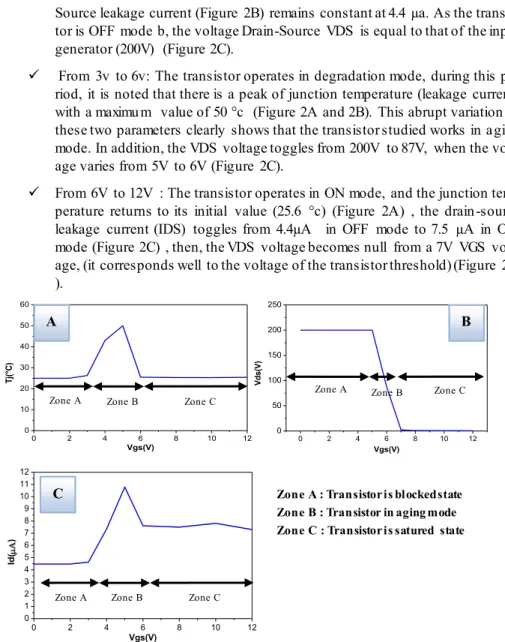
In order to validate the electro-thermal model of the transistor studied during this work. We used the transistor in a Power converter DC/DC Boost, which generates a power output of 3 KW. This study is based on the analysis of the behavior of the pa-rameters of the transistor, In the Pspice simulator, by varying the Gate-Source voltage (VGS) from the Transistor from0 to 10v. In Figure 2, we represented the junction tem-perature of the transistor studied and the drain-Source leakage current. The results ob-tained show that :
From 0v up to 3v: The transistor operates in a secure mode, the junction tem-perature of the transistor is in the range of 25 °c (Figure 2A). Then the
drain-V7 T D = 0 T F = 0.05u PW = 50u PER = 100u V1 = 12 T R = 0.05u V2 = 0 0 0 U1 C2M 0025120D D 1 G 2 S 3 T J 4 T C5 25Vdc V1 200 0 L 1 R1 5 0 C1 C2 D1 D1N5406
Source leakage current (Figure 2B) remains constant at 4.4 µa. As the transis-tor is OFF mode b, the voltage Drain-Source VDS is equal to that of the input generator (200V) (Figure 2C).
From 3v to 6v: The transistor operates in degradation mode, during this pe-riod, it is noted that there is a peak of junction temperature (leakage current) with a maximu m value of 50 °c (Figure 2A and 2B). This abrupt variation of these two parameters clearly shows that the transistor studied works in aging mode. In addition, the VDS voltage toggles from 200V to 87V, when the volt-age varies from 5V to 6V (Figure 2C).
From 6V to 12V : The transistor operates in ON mode, and the junction tem-perature returns to its initial value (25.6 °c) (Figure 2A) , the drain-source leakage current (IDS) toggles from 4.4µA in OFF mode to 7.5 µA in ON mode (Figure 2C) , then, the VDS voltage becomes null from a 7V VGS volt-age, (it corresponds well to the voltage of the transistor threshold) (Figure 2B ).
Fig. 2. Temperature junction (A) vs Vgs, Drain-source voltage Vds vs Vgs (B) and ° Drain-source leakage current vs Vgs vs Vgs (C)
2.2
Influence of the junction temperature variation on the transistor agingIn order to show the behavior of the transistor studied during this work, during its operation in aging mode, keeping the same application as that of the paragraph above. We have varied the junction temperature of the transistor from 0 ° C to 400 ° C, ex-ceeding the maximu m value of the temperature that can support the transistor, which is
0 2 4 6 8 10 12 0 10 20 30 40 50 60 Tj (° C ) Vgs(V) 0 2 4 6 8 10 12 0 50 100 150 200 250 V d s( V ) Vgs(V) 0 2 4 6 8 10 12 0 1 2 3 4 5 6 7 8 9 10 11 12 Id ( ) Vgs(V)
Zone A : Transistor is blocked state Zone B : Transistor in aging mode Zone C : Transistor is satured state Zone A Zone B Zone C
Zone A Zone B Zone C
Zone A Zone B Zone C
A B
4
of the order of 150 ° C. The different results obtained are shown in Figure 3. It appears that :
The source drain leakage current Ids of the transistor varies as a function of the junction temperature, the maximu m value is obtained at 225 ° C, it is of the order of 70.3μA. Beyond 225 ° C, by exceeding the maximu m value of the junction temperature supported by the transistor, the leakage current Ids de-creases. (Figure 3A).
The leakage current of the Ig gate remains almost constant from 25 ° C to 225 ° C, it varies around 70μA. Beyond 225 ° C., the leakage current Ig decreases until it vanishes at 400 ° C, (FIG. 3B).
The resistance Rdson is of no help for the transistor aging, even if one exceeds the supported temperature. It increases gradually as a function of the transistor junction temperature (FIG. 3C).
0 50 100 150 200 250 300 350 400 450 0 10 20 30 40 50 60 70 80 Id ( ) T(°C) 0 50 100 150 200 250 300 350 400 450 0 10 20 30 40 50 60 70 80 Ig ( ) T(°C) 0 50 100 150 200 250 300 350 400 450 0 30 60 90 120 150 180 210 240 R d so n (m ) T(°C)
Fig.3. Electrical quantities of the C2M0025120D transistor
A: Drain-source leakage Current, B: Grid leakage Current, C: Rdson resistance
A : Courant de fuite drain-source, B : Courant de fuite de la grille, C : Résistance Rdson.
A B
2.3
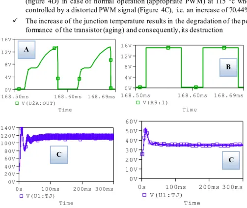
Influence of the change in grid-Source voltages VGS on the Aging of the transistorThe functioning of the transistors also depends on the quality of the control PWM signal, this may result in a degraded operation of the transistor. In order to clarify this point, keeping the same application of Figure 1, we control the transistor by a PWM signal completely distorted, this distortion is due to the absence of the driver between the control part and the power one ( Figure 4A), and another appropriate PWM signal using an 2111 driver (Figure 4B). Then, for each case, we plotted the resulting junction temperature (Figure 4C and D). All the results obtained show that:
The junction temperature of the C2M0025120D transistor increases by 34 °c (figure 4D) in case of normal operation (appropriate PWM) at 115 °c when controlled by a distorted PWM signal (Figure 4C), i.e. an increase of 70.44%. The increase of the junction temperature results in the degradation of the
per-formance of the transistor (aging) and consequently, its destruction
Figure 4: Influence of the PWM signal State on the aging of the C2M0025120D transis-tor
A and C: Distorted PWM Signal and the resulting junction temperature, B and D: PWM Signal and the resulting junction temperature
.
3
Conclusion
In this work, we studied an electro-thermal study of a power transistor based on silicon carbide C2M0025120D. This study consists of defining the different equations
Time 168.50ms 168.60ms 168.69ms V(U2A:OUT) 0V 4V 8V 12V 16V Time 168.50ms 168.60ms 168.69ms V(R9:1) 0V 4V 8V 12V 16V Time 0s 100ms 200ms 300ms V(U1:TJ) 0V 20V 40V 60V 80V 100V 120V 140V Time 0s 100ms 200ms 300ms V(U1:TJ) 0V 10V 20V 30V 40V 50V 60V A B C C
6
linking the different parameters of the transistor (VDS, IDS, Tj...), based on the electric and thermal model of the transistor developed during this work[1]. Then, we studied the aging of the transistor, by using the transistor in a DC/DC power converter, which generates a power output of 3 KW. The aging study is done by pushing the transistor to operate in particular conditions (temperature, drain current,...). From this study we deduced the behavior of the transistor by considering the electrical parameters (the drain-source leakage current, the junction temperature,...). The different results show that in aging mode, there are abrupt variations of some electrical parameters, which clearly shows that the electro-thermal model developed during this Work, for C2M0025120D transistor reflects well the reality.
References
1. K. Frifita, N. M’Sirdi, E. Baghaz, A. Naamane and M. Boussak
Electro-thermal Model of a of Silicon CarbidePower MOSFET In Proceedings of ICEERE 2018, Saadia -Morocco
2. Julio Brandelero, Bernardo Cougo, Thierry Meynard, Nicolas Videau, Olivier Goualard , Xavier Bonnin, Henri Schneider. Evaluation des pertes par commutation pour la conception des convertisseurset applications des composants grands gap.symposium de genie electrique (sge’14) : ef-epf-mge 2014, 8-9 juillet 2014, ens cachan, france.
3. Abderrazak LAKRIM, Driss TAHRI. The DC Behavioural Electrothermal Model of 4. Silicon Carbide Power MOSFETs under SPICE. IEEE International Conference on
Indus-trial Technology (ICIT), At Seville,Spain, Volume: 2818-2823,2015.
5. Shan Yin, Tao Wang, K. J. Tseng, Jiyun Zhao, Xiaolei Hu. Electro-Thermal Modeling of SiC Power Devices for Circuit Simulation. IEEE, 2013.
6. Nicolas Dubuc. modelisation electrothermique de transistors mesfet sic et optimisation d’une architecture doherty pour l’amplification de puissance a haut rendement . thèse de l’université de Limoges, 2003.
7. Matthias Bucher, Christophe Lallement and Christian C. Enz. An Efficient Parameter 8. Extraction Methodology for the EKV MOST Model. Proc. 1996 IEEE Int. Conference on
Microelectronic Test Structures, Vol. 9, pp. 145-150, Trento, Italy, March 26-28, 1996. 9. Bejoy N. Pushpakaran, Stephen B. Bayne, Gangyao Wang, John Mookken. fast andaccurate
electro-thermal behavioral model of a commercial sic 1200v, 80 mΩ power mosfet. ieee, 2015.
10. Rémy OUAIDA, Maxime BERTHOU , Pierre BROSSELARD , Sebastien OGE , Pascal Bevilacqua , Charles Joubert.Etude sur les transistors MOSFETs enCarbure de Silicium – Potentiel d’utilisation dans les Applications Hautes Températures.
11. Zheng Chen. Electrical Integration of SiC Power Devices for High-Power-Density Applica-tions.Institut polytechnique Doctorat de l’Université d'État de Virginie, 26Sept 2013, Etat Unis.
12. Thomas Santini. Contribution à l'étude de la fiabilité des MOSFETs en carbure de Silicium. Thèse de doctorat de l’université de Lyon, 25/03/2016, France.
13. Rémy Ouaida. Vieillissement et mécanismes de dégradation sur des composants de puis-sance en carbure de silicium (SIC) pour des applications haute température. Thèse de doc-torat L’université Lyon 1, 29 Octobre 2014, France.