RESEARCH OUTPUTS / RÉSULTATS DE RECHERCHE
Author(s) - Auteur(s) :
Publication date - Date de publication :
Permanent link - Permalien :
Rights / License - Licence de droit d’auteur :
Bibliothèque Universitaire Moretus Plantin
Institutional Repository - Research Portal
Dépôt Institutionnel - Portail de la Recherche
researchportal.unamur.be
University of Namur
Stability of edge magnetism against disorder in zigzag MoS2 nanoribbons
Vancsó, Péter; Hagymasi, Imre; Castenetto, Pauline; Lambin, Philippe
Published in:Physical Review Materials
DOI:
10.1103/PhysRevMaterials.3.094003
Publication date:
2019
Document Version
Publisher's PDF, also known as Version of record
Link to publication
Citation for pulished version (HARVARD):
Vancsó, P, Hagymasi, I, Castenetto, P & Lambin, P 2019, 'Stability of edge magnetism against disorder in zigzag MoS2 nanoribbons', Physical Review Materials, vol. 3, no. 9, 094003.
https://doi.org/10.1103/PhysRevMaterials.3.094003
General rights
Copyright and moral rights for the publications made accessible in the public portal are retained by the authors and/or other copyright owners and it is a condition of accessing publications that users recognise and abide by the legal requirements associated with these rights. • Users may download and print one copy of any publication from the public portal for the purpose of private study or research. • You may not further distribute the material or use it for any profit-making activity or commercial gain
• You may freely distribute the URL identifying the publication in the public portal ? Take down policy
If you believe that this document breaches copyright please contact us providing details, and we will remove access to the work immediately and investigate your claim.
P´eter Vancs´o,1, 2 Imre Hagym´asi,3, 4 Pauline Castenetto,2 and Philippe Lambin2
1
2D Nanoelectronics ”Lend¨ulet” Research Group, Institute of Technical Physics and Materials Science, HAS Centre for Energy Research, 1121 Budapest, Hungary
2
Department of Physics, University of Namur, 61 rue de Bruxelles, 5000 Namur, Belgium
3Department of Physics and Arnold Sommerfeld Center for Theoretical Physics,
Ludwig-Maximilians-Universit¨at M¨unchen, D-80333 M¨unchen, Germany
4
Strongly Correlated Systems ”Lend¨ulet” Research Group, Institute for Solid State Physics and Optics, HAS Wigner Research Centre for Physics, 1121 Budapest, Hungary
Molybdenum disulfide nanoribbons with zigzag edges show ferromagnetic and metallic properties based on previous ab-initio calculations. The investigation of the role of disorder on the magnetic properties is, however, still lacking due to the computational costs of these methods. In this work we fill this gap by studying the magnetic and electronic properties of several nanometer long MoS2
zigzag nanoribbons using tight-binding and Hubbard Hamiltonians. Our results reveal that proper tight-binding parameters for the edge atoms are crucial to obtain quantitatively the metallic states and the magnetic properties of MoS2 nanoribbons. With the help of the fine-tuned parameters, we
perform large-scale calculations and predict the spin domain-wall energy along the edges, which is found to be significantly lower compared to that of the zigzag graphene nanoribbons. The tight-binding approach allows us to address the effect of edge disorder on the magnetic properties. Our results open the way for investigating electron-electron effects in realistic-size nanoribbon devices in MoS2 and also provide valuable information for spintronic applications.
I. INTRODUCTION
Electronic and spintronic applications of two dimen-sional (2D) materials are in the focus of scientific attention.1–6 Transition metal dichalcogenides (TMDs),
and particularly molybdenum disulfide (MoS2), are one
of the most intensively studied materials due their di-rect band gaps,4,7 which make them good candidates for
optical8 and electronic applications such as transistors9
or even microprocessors.10 MoS
2 is a nonmagnetic
semi-conductor, however, several theoretical studies11–13
re-ported magnetic moments on the edges of zigzag MoS2
nanoribbons similar to the case of zigzag graphene nanoribbons.14,15These density functional theory (DFT)
calculations revealed ferromagnetic and metallic behav-ior of the edges, furthermore the emerged magnetism was still preserved in several edge reconstructed and passivated systems independent from the nanoribbons width.11,16–18 In the last years, impressive advances on
the sample preparation were reported. MoS2
nanorib-bons with nanometer width and well-defined edges have been synthetized by using bottom-up19,20 and
top-down21,22 techniques. In addition, magnetic measure-ments on large scale epitaxial growth of zigzag MoS2
nanoribbons show prominent ferromagnetic behavior.23
Due to these recent experimental results theoretical un-derstanding of the edge magnetism in MoS2nanoribbons
is quite important, especially in larger, realistic systems including disorder.
In the case of zigzag graphene nanoribbons different spintronic applications were proposed based on the ap-peared magnetic moments along the edges.24–27
How-ever, it has turned out that the computational cost of ab-initio calculations does not allow the investigation of
graphene nanoribbons in realistic size with disorder. In order to study systems involving a large number of atoms, tight-binding (TB) approach is a more suitable alterna-tive, which can also provide a simple starting point for the further inclusion of many-body electron-electron ef-fects. By using TB parameters and local Coulomb in-teraction (the so-called Hubbard-U ) the magnetic prop-erties of the graphene nanoribbons were studied in large scale systems.28–31 It was found that the magnetism of the edge states is robust against disorder and potential fluctuations. However, as far as we know, similar inves-tigation of the magnetic properties of MoS2nanoribbons
has not been performed yet.
Nowadays, a wide range of TB parameters is available for TMDs including MoS2 monolayers.32–35 These
mod-els accurately reproduce the DFT band structure calcu-lations near the conduction and valence bands, provid-ing a key tool for further studies of electronic and trans-port properties in larger systems. In the case of MoS2
nanoribbons several papers examined the electronic and transport properties based on the monolayer MoS2 TB
parameters.36–41 Besides the important observations of
these works, none of them takes into account the differ-ent environmdiffer-ent of the edge atoms compared to the inner atoms of the nanoribbon during the TB parametrization. Therefore, the obtained band structures of the nanorib-bons, where all of the Mo and S atoms are handled equally, show only qualitative agreement with the DFT band structure calculations. Namely, the TB calculations display metallic properties of the zigzag nanoribbons, but even the number of the metallic bands is different com-pared to the DFT results. However, in order to describe the proper magnetic properties of the nanoribbons, the accurate treatment of the edge states is crucial, since the
2 magnetism originates from the splitting of the metallic
edge states.
In this paper we demonstrate that the metallic states of zigzag MoS2nanoribbons can be reproduced with their
proper orbital characters by adapting TB parameters for the edge atoms. These results provide us a starting point for further inclusion of the electron-electron interactions, where the Coulomb repulsion is taken into account by using local Hubbard interaction terms in the fine-tuned TB Hamiltonian. This Hubbard model within the mean-field approximation, applied for the first time to MoS2
nanoribbons, circumvents the computational bottleneck of ab-initio calculations. Our results show that this sim-ple model is not only capable of describing the magnetism in MoS2 nanoribbons with zigzag edges, but also gives
quantitatively accurate results for the magnetization val-ues compared to DFT calculations. As a next step, we extend our calculations to several nanometer long ribbon containing 800 atoms. We have found that the domain-wall energies are much lower compared to those of the graphene nanoribbons,42 which predicts fluctuations of
spins along the ribbon edge. We also investigated short-and long-range disorder originating from inhomogeneous charge distribution of the substrate or other structural imperfections.
The paper is organized as follows. In Sec. II. we present the applied theoretical models for MoS2
nanorib-bons with zigzag edges. In Sec. III. A we compare the TB and DFT calculations of the electronic and magnetic properties of the nanoribbons. In Sec. III. B we applied our method for several nanometer long nanoribbons and analyze the spin domain wall. Sec. III. C presents the ef-fects of the short and long-range disorder on the magnetic properties. Finally, we show our conclusions in Sec. IV.
II. METHODS
Band structure calculations of the zigzag MoS2
nanoribbon (Fig. 1) are performed by using DFT and TB calculations. As Capuletti et al.33pointed out an
eleven-orbital TB model within Slater-Koster scheme43 is able
to reproduce the band structure of the single layer MoS2.
This model considers an orthogonal basis composed of five orbitals (4dxy, 4dyz, 4dxz, 4dx2−y2, 4d3z2−r2) for each molybdenum (Mo) atom and three orbitals (3px, 3py,
3pz) for each sulfur (S) atom resulting in z-symmetric
and z-antisymmetric states. In the case of our zigzag nanoribbon calculations, we follow the method and use the TB parameters (hopping terms and on-site energies) described in Ref. [33] as a starting point. In the next step, we modify the on-site energy parameters of the edge atoms in the ribbon (Table I) in order to quantitatively reproduce the DFT band structure results.
DFT calculations are carried out using the projector augmented wave (PAW) method44 as implemented in the Vienna ab initio simulation package (VASP).45 The generalized gradient approximation of Perdew–Burke–
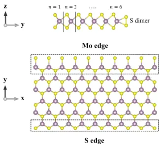
Mo edge S edge y x y S dimer 𝑛𝑛 = 1 𝑛𝑛 = 2 …. 𝑛𝑛 = 6 z y
FIG. 1. Side and top view of the relaxed geometry of zigzag MoS2nanoribbon with sulfur dimer passivation along the Mo
edge. Purple and yellow spheres represent molybdenum and sulfur atoms, respectively. The edge regions, where TB pa-rameters of the atoms are modified marked by the dotted black lines.
Ernzerhof (GGA-PBE) is adopted for the exchange-correlation (XC) functional.46 The band structure
cal-culations are performed with plane wave cutoff of 500 eV and the Brillouin zone is sampled with (12 × 12 × 1) Monkhorst-Pack mesh of k-points.47 During geometry
optimization, the convergence criterion for forces is set to 0.01 eV/˚A.
To describe the magnetic properties of the zigzag nanoribbons with the help of the modified TB parameters we use a grand-canonical ensemble and switch on Hub-bard interaction terms with different amplitudes, UMo,
US corresponding to the five Mo and three S orbitals,
respectively: H = X hijiσ tijˆc†iσˆcjσ+ UMo X i∈Mo ˆ ni↑ˆni↓ +US X i∈S ˆ ni↑ˆni↓− X iσ (εi− µ)ˆniσ. (1)
Here tij encodes the hopping TB parameters, ciσ
annihi-lates a fermion at site i with spin σ, εiare the fine-tuned
on-site energy parameters, niσis the particle-number
op-erator, and µ is the chemical potential. The summation in the two Hubbard terms extends over the Mo or S sites only. In the case of the long nanoribbons our system con-sists of 800 atoms and nearly 3000 fermionic sites, at a rate of one site per atomic orbital. Such a large system can be solved only using some kind of approximation. We apply the standard mean-field decoupling of the Hubbard terms: ni↑ni↓ ≈ hni↑ini↓+ ni↑hni↓i − hni↑ihni↓i which
gives us an effective single-particle Hamiltonian that can be diagonalized either in k- or real space self-consistently.
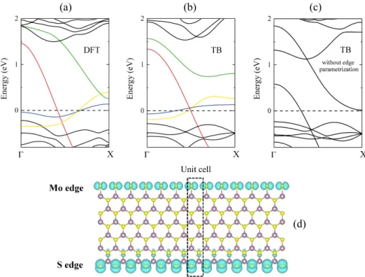
(a) (b) (c)
(d)
FIG. 2. Non spin-polarized band structure calculations of the zigzag MoS2 nanoribbon (n = 6). (a) DFT calculation, (b) TB
calculation using the modified TB parameters for the edge atoms. Mid-gap states originated from the edge atoms are marked by different colors. States with blue and green colors correspond to the S edge, while red and yellow colors correspond to the Mo edge. (c) TB calculations without edge parametrization. (d) Charge density plots around the Fermi-level calculated by DFT. The isovalue is set to be 2 × 10⁻³e/˚A3.
The chemical potential is also determined in each itera-tion step by requiring that the electron number per unit cell should give the same number as in the nonmagnetic case. The iteration is stopped if the difference between the electron densities decreases below 10−6.
III. NUMERICAL RESULTS AND DISCUSSION
A. Band structure calculations of the nanoribbon In Fig. 1 we can see the top and side view of the geom-etry of MoS2 nanoribbon (n = 6) with zigzag edges. The
width parameter n is defined as the number of zigzag lines across the nanoribbon as defined analogously for the case of graphene nanoribbons. Without edge passi-vation, zigzag nanoribbons have two types of edges, one is S-terminated, while the opposite one is Mo-terminated. However, both theoretical predictions and experimental observations found the pure Mo edge energetically un-favoured compared to edge passivated geometries.48,49
In order to model realistic nanoribbon geometries in our calculations, we use the experimentally observed sulfur dimers passivation at the Mo edge. After the relaxation of the geometry, the S-S bond length of the dimer is found to be 1.99 ˚A, significantly differ from the in-plane (3.18 ˚
A) and out-of-plane (3.13 ˚A) S-S bond lengths.
The unit cell band structure calculations of the nanoribbon (n = 6) without spin polarization are shown in Fig. 2. From the DFT calculations (Fig. 2(a)) four mid-gap states can be seen that are highlighted by differ-ent colors. Three of them cross the Fermi level, implying the existence of metallic states in agreement with pre-vious results.48,50 These metallic states are almost
com-pletely localized on the S and Mo edge of the nanoribbon (Fig. 2(d)). More precisely, the Kohn-Sham wave func-tions reveal that the states marked by blue and green colors correspond to the localized states of the S and Mo atoms at the S edge, while the states with red and yellow colors originate from S dimers and Mo atoms at the Mo edge. From the charge density plot around the Fermi-level (Fig. 2(d)) it is also visible that in the Mo edge side the S dimers have pxorbital character in contrast to the S
edge side, where the pzorbitals of the S atoms dominate,
forming one-dimensional metallic states along the edges. By exploiting our modified TB parameters (Table I) in the edge regions (Fig. 1 dotted area), we are able to re-produce the shape and the number of the metallic states with their proper orbital character (Fig. 2(b)). In con-trast, the band structure results without our fine-tuning for the edge atoms (Fig. 2(c)) show significantly different edge states compared to the DFT results highlighting the importance of the proper treatment of the edges within the TB formalism. We have also examined the electronic
4
- Mo atom S atom S dimer
Mo edge -2.03, 1.42, 1.42, 0.28,-8.28, -12.24 -0.55, -5.28,-8.24 -4.03, 0.51
S edge -2.03, 4.30, -0.80, -1.90, 0.18, -6.50 --12.03, -2.60
TABLE I. Modified tight-binding on-site energy parameters for the edge atoms (marked by the dotted black lines in Fig. 1) in units of eV. Values corresponds to the five orbitals (dxy,
dyz, dxz, dx2−y2, d3z2−r2) for Mo atoms, and three orbitals (px, py, pz) for S atoms, respectively. On-site energies and
the hopping terms for the inner atoms of the nanoribbons are given in Ref. [33].
interaction between the two edges of the nanoribbon. We perform the same calculations on a double size (n = 12) nanoribbon (Fig. 3), where the mid-gap states show ex-actly the same behavior. Our results have verified that the edges states can be treated independently even in the case of the narrower (n = 6) nanoribbon. In other words, the electronic states at the S edge and Mo edge do not interact with each other for nanoribbons having n ≥ 6, which implies that our TB parametrization of the edges is able to describe wider ribbons electronic properties as well.
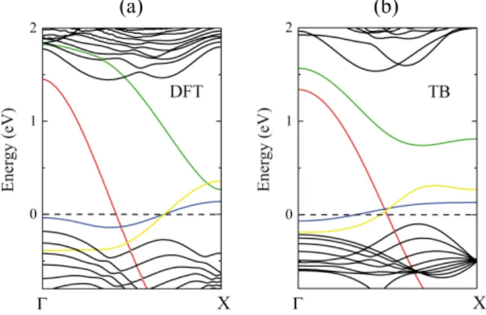
(a) (b)
FIG. 3. Non spin-polarized band structure calculations of the zigzag MoS2 nanoribbon (n = 12). (a) DFT calculation
(b) TB calculation using the modified TB parameters for the edge atoms. Mid-gap states (marked by different colors) are the same compared to narrower (n = 6) nanoribbon implying negligible electronic interaction between the Mo and S edges. As a next step, we apply the Hubbard-model, Eq. (1), by using our modified TB parameters to obtain the mag-netic properties of the nanoribbons. The Hubbard in-teraction terms for the S and Mo atoms are defined by comparing the results with spin polarized DFT calcu-lations. Figure 4 presents the results of the two cal-culations, where US = 1.7 eV and UMo = 0.6 eV
val-ues are applied in the Hubbard calculations. According to both methods localized magnetic moments appear on the S edge, which result from the spin splitting of the flat band of the edge S atoms (marked by blue color in
-1 0 1 Ene rgy ( eV) DFT 0.58 eV Γ X -1 0 1 E Hubbard Ene rgy ( eV) Γ X 0.52 eV E (a) (b)
FIG. 4. Spin-polarized band structure calculations of the zigzag MoS2 nanoribbon (n = 6) by using (a) DFT and (b)
Hubbard-model with US= 1.7 eV and UMo= 0.6 eV
param-eters. Red and black curves correspond to the up and down spins, respectively. The Fermi level is at zero energy. Magne-tization appears from the splitting of the band of the S atom resulting localized magnetic moments along the S edge.
Fig. 2 (a)-(b)). In more detailed, the higher value of density of states and the finite Coulomb repulsion lead-ing to Stoner instability and splits the partially occupied S atom band into a totally filled spin-down (↓) and an al-most empty spin-up (↑) band. By using the appropriate U values, the large 0.52 eV splitting of the band and the local magnetic moments M = 1/2(n↑− n↓)geµB ≈ 0.35
µB on the S atoms at the S edge (both in the upper
and bottom layer) are predicted from the Hubbard cal-culations in excellent agreement with the DFT results (M = 0.32 µB). We note that the metallic state from
the S atom, which plays the major role in the magnetiza-tion, is completely missing in the non-parametrized TB results (Fig. 2(c)). From our spin-polarized calculations only the S edge exhibits magnetic properties, in contrast to the previous DFT calculation with unpassivated Mo edge.11The vanishing magnetic values at the Mo edge in our nanoribbon geometry are due to the S dimers passi-vation. Therefore, in the following sections we focus on the magnetic properties of the S edge.
B. Spin domain wall
As we demonstrated in the previous section, with the help of proper TB parametrization at the edges both the electronic and magnetic properties of a zigzag nanorib-bon can be obtained. Using the results of the unit cell cal-culations, we extend the system size and investigate the magnetic properties of a 40 unit cell long (Lx= 12.8 nm)
nanoribbon within the framework of the Hubbard model. First we study collinear domain walls at the S edge by rotating the half of the spins in the supercell geometry. Fig. 5 illustrates the distribution of the spin density for the ferromagnetic ground state (Fig. 5(a)) and the
ex-5 10 15 20 25 30 35 40 -0.4 -0.2 0.0 0.2 0.4 M ( � Β ) site number(Nx)
E
dw=
+6.5 meV(a)
(b)
(c)
FIG. 5. Spin density plot of the zigzag MoS2 nanoribbon. (a) Top view of the ferromagnetic ground state and (b) the collinear
domain wall excitation at the S edge. Blue and red circles correspond to spin-up and spin-down electrons, respectively. (c) Magnetic moments at the edge on the S atoms in the presence of the domain wall. For comparison red dotted line shows the ground state magnetic values.
cited state including collinear domain walls (Fig. 5(b)). The spin densities of the S atoms at the S edge (both in the upper and bottom layer) show that the domain wall is practically localized within one unit cell (0.3 nm) and the magnetization displays weak oscillations around the tran-sition place (Fig. 5(c)). Surprisingly, we found that the collinear domain wall creation energy is only Edw= +6.5
meV, which is more than one magnitude lower compared to case of zigzag graphene nanoribbons, Edw = +114
meV.42 The strong localization and the low energy of the domain wall together indicate weak magnetic cou-pling along the S edge. In order to estimate the magnetic coupling, we calculate the quadratic energy-wave vector dispersion relation, E(q) = Dq2 with the spin wave
ex-change stiffness constant, D. From the different q vector calculations, the spin stiffness constant is found to be D = 161 meV˚A2, which is around a half compared to
zigzag graphene nanoribbons, D = 320 meV˚A2.42
An explanation of the weak coupling in the system compared to zigzag graphene nanoribbons is related to the different geometries and electronic properties of the two materials. About the geometry, the zigzag S edge atoms distance is 3.18 ˚A, larger than in the case of graphene nanoribbons’ C atoms distance (2.46 ˚A), which is able to reduce the interaction between the edge atoms in MoS2. The nearest neighbor atoms, which can also
mediate magnetic coupling between the edge atoms, are C atoms in graphene, while Mo atoms for MoS2. The
magnetic coupling through the middle layer Mo atom can differ from the coupling through the in-plane C atom in graphene. Besides the differences in the edge geometries, there are also discrepancies between the electronic prop-erties. The edge states in zigzag graphene nanoribbons show almost flat bands in contrast to MoS2, where the
S atom bands have a small, but finite energy dispersion (Fig. 2). The higher density of states due to the flat bands can significantly strengthen the electron-electron interaction effects and thus the magnetic coupling in the case of graphene nanoribbons. We also verified the weak coupling by performing DFT calculations in a double unit cell geometry of zigzag MoS2 nanoribbon. The states
with ferromagnetic (↑↑) and antiferromagnetic (↑↓) spin ordering at the edges show only 14 meV difference in energy. It is worth noting that the small energy values between the ferromagnetic and antiferromagnetic states were reported in zigzag WS2 nanoribbons,51 which also
emphasizes the similar magnetic mechanisms in layered structures of MoS2 and WS2.
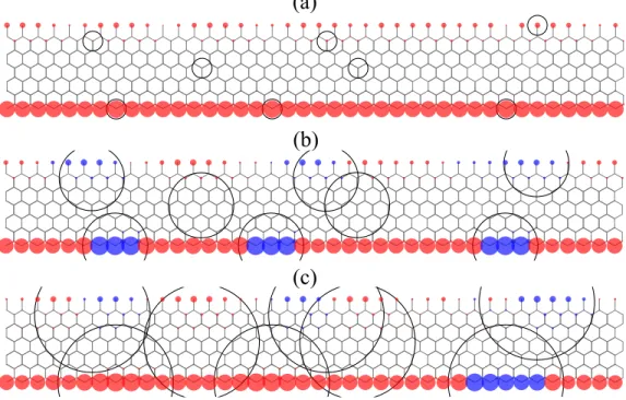
C. Zigzag nanoribbon with disorder
Defects and disorder can significantly modify the in-trinsic properties of the materials. In the case of zigzag MoS2 nanoribbons, transport calculations have revealed
6
(a)
(b)
(c)
FIG. 6. Spin density plot in the presence of disorder. (a)-(c) Top view of the magnetic ground states of the zigzag nanoribbons by using Gaussian potentials with V0= +100 meV and different width parameters c = 1, 3, 5 in ˚Angstr¨om. Black circles denote
the positions of the randomly distributed potentials. The radius of the circles corresponds to the size of the potentials. Blue and red circles correspond to spin-up and spin-down electrons, respectively.
disorder.40,41,52 Motivated by the observed weak
mag-netic coupling at the S edge, we investigate the robust-ness of the magnetization against short- and long-range disorder.
In order to model disorder in the system we apply Gaussian potentials to the on-site energy parameters on each site: V (r) = N X i=1 V0e−|r−ri| 2/2c2 , (2)
where ri are the positions of the disorder, V0 and c are
Gaussian parameters corresponding to the strength and the range of the disorder, respectively. In the case of specific defects, such as vacancies or adatoms, the on-site and the hopping parameters of the TB model should be modified to describe the defect properties. However, by using the combination of our edge parametrization and Gaussian potentials, we are able to examine both short-and long-range disorder in the system without further modifications of the TB parameters. This disorder po-tential can be also regarded as an inhomogeneous charge distribution of the substrate.53
We use randomly distributed potentials in the sys-tem (N = 8), which contains disorder along the edges and also the inner part of the nanoribbon (marked by the center of the black circles in Fig. 6). Gaussian po-tentials with V0 = +100 meV are considered
accord-ing to often observed n-doped behavior of MoS2
sam-ples on substrates.54,55Fig. 6 shows the calculated
mag-netic ground state of the system for c = 1, 3, 5 values in ˚
Angstr¨om, which corresponds to disorder localized from one atom to extended defects above nanometer size.
In Fig. 6(a), we can recognize the ferromagnetic ground state at the S edge for the case of the strongly localized perturbation potentials (c = 1 ˚A). We found that the disorder localized in the middle of the nanoribbon does not affect the magnetic properties, while the disorder on the S atoms at the S edge causes slightly increased mag-netic moments from the M = 0.35 µB defect-free value
to M = 0.41 µB. The growth of the magnetic moments
of the S atoms, where the potentials are centered, can be understood from Fig. 4b. The positive potential causes positive shift of the bands in energy, therefore the par-tially filled spin-up band of the S atoms at the edge be-comes less occupied. The spin-down band is far from the Fermi-level, therefore it remains totally occupied in the presence of the potential resulting higher magnetic moments for the S atoms. Overall, we can say that shift-ing the bands of the S atoms due to positive or negative potential leads to increased or decreased magnetic mo-ments at the edges compared to the defect-free system. In contrast to the previous c = 1 ˚A result, the potential with c = 3 ˚A parameter extending more than 3 atom dis-tances, cause significant changes on the magnetic ground state (Fig. 6(b)). Most importantly, in regions, where the potentials are applied, the orientation of the magnetic moments has been changed (M = −0.47 µB). The lower
ferromag-netic state implies that potentials act in a more complex way than in the previous c = 1 ˚A case. The potentials modify both the Mo and S atoms bands in the potential region resulting in the formation of domain walls along the edges. Similar changes of the magnetic moments can be seen at the Mo edge, where the S dimers have signifi-cantly smaller magnetic moments (M = ±0.05 µB).
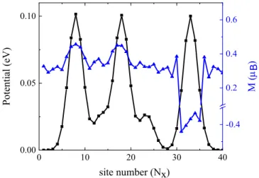
Fur-ther increasing of the radius of the individual Gaussian potentials (c = 5 ˚A) leads to overlapping regions in the potential at the edges (Fig. 6c). The magnetic calcula-tions reveal that in the case of the overlapping region the ferromagnetic ground state is restored at the S edge. In contrast, domain walls appear in non-overlapping region in the S edge. The relation between the potential and magnetic texture is visible in Fig. 7. This result implies that besides the width, the profile of the potential plays also an important role on the magnetic ground state of the system. 0 10 20 30 40 0.00 0.05 0.10 site number (Nx) Pot ent ial (e V ) -0.4 0.2 0.4 0.6 M (�Β )
FIG. 7. Potential profile and magnetic moments along the S edge. Black and blue curves correspond to the potential (c = 5 ˚A) and magnetic values on the S atoms at the S edge. The magnetic moments are following the potential pro-file. Ferromagnetic orientation of the spins occurs, where the Gaussian potentials have overlapping region, while domain walls appear in the non-overlapping region.
In conclusion, our calculations including disorder high-light significant changes on magnetic ground state in zigzag MoS2 nanoribbons. For short range disorder the
values of the magnetic moments have been changed, but the ferromagnetic arrangement is still conserved. By in-creasing the disorder range not only the values, but also the direction of the moments is modified yielding spin do-main walls, which are also sensitive to the profile of the potential. The energy differences of the ground states and excited states in the different disorder are in the or-der of tens meV in the system. This behavior can be qual-itatively understood if we assume that the edge magnetic moments can be described by a one-dimensional Ising model, as it was shown for graphene with zigzag edges.42 In this case, the effects of the disorder resemble to what the random fields cause in the Ising model, where also
for-mation of domain walls in the system was predicted.56–58 In those systems, the creation of the domain wall is de-termined by an interplay of the domain wall energy and the properties of the applied field. It seems that in our case the properties of the disorder potential play a similar role. The possibility to modify the spin-texture by po-tential disorder can be useful for spintronic applications. By applying periodic or non-periodic potentials at the edge, the magnetic moments can be tuned realizing vari-ous magnetic ground states. Furthermore, even dynami-cal control of the edge magnetic moments can be achieved with local probe techniques (eg. conducting AFM tip), where the tip induced potential flips the edge moments at the location of the tip. By moving the tip along the edge, one could move the induced reversed magnetic domain.
IV. CONCLUSIONS
Magnetic properties of 2D materials continue to pose a great interest both from fundamental and application point of view. In this paper, we reported magnetic cal-culations for MoS2 nanoribbons with zigzag edges based
on the Hubbard model. We demonstrated that proper TB parametrization of the edge atoms is crucial in or-der to describe the magnetic properties of the nanorib-bons. Using our fine-tuned TB parameters and Hub-bard interaction strength, we have investigated a several nanometer long ribbon and calculated the spin domain-wall energy. The observed low domain-domain-wall energy indi-cates weak magnetic coupling between the S atoms at the edge in contrast to zigzag graphene nanoribbons. By using randomly distributed Gaussian potentials we have also revealed the effect of the disorder on the mag-netic properties. We have shown that the magnetic ground state strongly depends on the potential parame-ters, where even disorder with few atomic distances can change the orientation of the edge spins. While these findings reveal the importance of reducing the disorder in MoS2nanoribbons (for example by encapsulating the
ribbons with hexagonal boron nitride), this feature can be also exploited to manipulate the spin-texture by an ap-plied potential field. Our approach presented here opens the way for investigating electron-electron effects in large scale MoS2 and other TMD materials, which is essential
for spintronic applications.
ACKNOWLEDGMENTS
P. V. and I. H. contributed equally to this work. The work has been supported by the NanoFab2D ERC Starting Grant, the Graphene Flagship, H2020 Graphene Core2 project no. 785219, the H2020 MCA-RISE ”Infu-sion” project no. 734834 and the Korea Hungary Joint Laboratory for Nanosciences. P. V. acknowledges the Hungarian National Research, Development and Innova-tion Office (Hungary) Grant No. KH130413. I. H. was
8 supported by the Alexander von Humboldt Foundation
and in part by Hungarian National Research, Develop-ment and Innovation Office through Grant No. K120569 and the Hungarian Quantum Technology National Ex-cellence Program (Project No.
2017-1.2.1-NKP-2017-00001). The research used resources of the Plateforme Technologique de Calcul Intensif (PTCI) located at the University of Namur, which is supported by the FNRS-FRFC under Conventions No. 2.4520.11.
1 P. Avouris, Nano Lett. 10, 4285 (2010). 2
W. Han, R. K. Kawakami, M. Gmitra, and J. Fabian, Nat. Nanotechnol. 9, 794 (2014).
3 S. Roche, J. Akerman, B. Beschoten, J.-C. Charlier,
M. Chshiev, S. P. Dash, B. Dlubak, J. Fabian, A. Fert, M. H. D. Guimaraes, F. Guinea, I. Grigorieva, C. Schoe-nenberger, P. Seneor, C. Stampfer, S. O. Valenzuela, X. Waintal, and B. van Wees, 2D Mater. 2, 030202 (2015).
4
O. V. Yazyev and A. Kis, Mater. Today 18, 20 (2015).
5
N. Zibouche, A. Kuc, J. Musfeldt, and T. Heine, Ann. Phys. (Berlin) 526, 395 (2014).
6
W. Han, APL Mater. 4, 032401 (2016).
7
K. F. Mak, C. Lee, J. Hone, J. Shan, and T. F. Heinz, Phys. Rev. Lett. 105, 136805 (2010).
8
A. Splendiani, L. Sun, Y. Zhang, T. Li, J. Kim, C.-Y. Chim, G. Galli, and F. Wang, Nano Lett. 10, 1271 (2010).
9 B. Radisavljevic, A. Radenovic, J. Brivio, V. Giacometti,
and A. Kis, Nat. Nanotechnol. 6, 147 (2011).
10
S. Wachter, D. K. Polyushkin, O. Bethge, and T. Mueller, Nat. Commun. 8, 14948 (2017).
11 Y. Li, Z. Zhou, S. Zhang, and Z. Chen, J. Am. Chem. Soc.
130, 16739 (2008).
12
A. R. Botello-Mendez, F. Lopez-Urias, M. Terrones, and H. Terrones, Nanotechnology 20, 325703 (2009).
13
A. Vojvodic, B. Hinnemann, and J. K. Norskov, Phys. Rev. B 80, 125416 (2009).
14 M. Fujita, K. Wakabayashi, K. Nakada, and K. Kusakabe,
J. Phys. Soc. Jpn. 65, 1920 (1996).
15
Y.-W. Son, M. L. Cohen, and S. G. Louie, Phys. Rev. Lett. 97, 216803 (2006).
16
R. Shidpour and M. Manteghian, Nanoscale 2, 1429 (2010).
17
C. Ataca, H. Sahin, E. Akturk, and S. Ciraci, J. Phys. Chem. C 115, 3934 (2011).
18 H. Pan and Y.-W. Zhang, J. Mater. Chem. 22, 7280 (2012). 19
S. Li, Y.-C. Lin, W. Zhao, J. Wu, Z. Wang, Z. Hu, Y. Shen, D.-M. Tang, J. Wang, Q. Zhang, H. Zhu, L. Chu, W. Zhao, C. Liu, Z. Sun, T. Taniguchi, M. Osada, W. Chen, Q.-H. Xu, A. T. S. Wee, K. Suenaga, F. Ding, and G. Eda, Nat. Mater. 17, 535 (2018).
20 C. Yang, B. Wang, Y. Xie, Y. Zheng, and C. Jin,
Nan-otechnology 30, 255602 (2019).
21
X. Liu, T. Xu, X. Wu, Z. Zhang, J. Yu, H. Qiu, J.-H. Hong, C.-H. Jin, J.-X. Li, X.-R. Wang, L.-T. Sun, and W. Guo, Nat. Commun. 4, 1776 (2013).
22
A. A. Koos, P. Vancso, G. Z. Magda, Z. Osvath, K. Kertesz, G. Dobrik, C. Hwang, L. Tapaszto, and L. P. Biro, Carbon 105, 408 (2016).
23
R. Qi, S. Wang, M. Wang, W. Liu, Z. Yan, X. Bi, and Q. Huang, Chem. Commun. 53, 9757 (2017).
24 Y.-W. Son, M. L. Cohen, and S. G. Louie, Nature 444,
347 (2006).
25
W. Y. Kim and K. S. Kim, Nat. Nanotechnol. 3, 408 (2008).
26 M. Zeng, L. Shen, M. Zhou, C. Zhang, and Y. Feng, Phys.
Rev. B 83, 115427 (2011).
27
M. Zeng, L. Shen, H. Su, C. Zhang, and Y. Feng, Appl. Phys. Lett. 98, 092110 (2011).
28
H. U. Ozdemir, A. Altintas, and A. D. Guclu, Phys. Rev. B 93, 014415 (2016).
29 J. P. C. Baldwin and Y. Hancock, Phys. Rev. B 94, 165126
(2016).
30
P. Vancso, I. Hagymasi, and L. Tapaszto, 2D Mater. 4, 024008 (2017).
31 K. E. Cakmak, A. Altintas, and A. D. Guclu, Phys. Rev.
B 98, 115428 (2018).
32
F. Zahid, L. Liu, Y. Zhu, J. Wang, and H. Guo, AIP Adv. 3, 052111 (2013).
33
E. Cappelluti, R. Roldan, J. A. Silva-Guillen, P. Ordejon, and F. Guinea, Phys. Rev. B 88, 075409 (2013).
34 R. Roldan, M. P. Lopez-Sancho, F. Guinea, E. Cappelluti,
J. A. Silva-Guillen, and P. Ordejon, 2D Mater. 1, 034003 (2014).
35 E. Ridolfi, D. Le, T. S. Rahman, E. R. Mucciolo, and C. H.
Lewenkopf, J. Phys. Condens. Matter 27, 365501 (2015).
36
R.-L. Chu, G.-B. Liu, W. Yao, X. Xu, D. Xiao, and C. Zhang, Phys. Rev. B 89, 155317 (2014).
37 H. Rostami, R. Roldan, E. Cappelluti, R. Asgari, and
F. Guinea, Phys. Rev. B 92, 195402 (2015).
38
H. Rostami, R. Asgari, and F. Guinea, J. Phys. Condens. Matter 28, 495001 (2016).
39
A. Heshmati-Moulai, H. Simchi, M. Esmaeilzadeh, and F. M. Peeters, Phys. Rev. B 94, 235424 (2016).
40 F. W. N. Silva, A. L. M. T. Costa, L. Liu, and E. B.
Barros, Nanotechnology 27, 445202 (2016).
41
E. Ridolfi, L. R. F. Lima, E. R. Mucciolo, and C. H. Lewenkopf, Phys. Rev. B 95, 035430 (2017).
42 O. V. Yazyev and M. I. Katsnelson, Phys. Rev. Lett. 100,
047209 (2008).
43
J. C. Slater and G. F. Koster, Phys. Rev. 94, 1498 (1954).
44 P. Blochl, Phys. Rev. B 50, 17953 (1994). 45
G. Kresse and J. Hafner, Phys. Rev. B 47, 558 (1993).
46
J. Perdew, K. Burke, and M. Ernzerhof, Phys. Rev. Lett. 77, 3865 (1996).
47
H. Monkhorst and J. Pack, Phys. Rev. B 13, 5188 (1976).
48
M. Bollinger, J. Lauritsen, K. Jacobsen, J. Norskov, S. Helveg, and F. Besenbacher, Phys. Rev. Lett. 87, 196803 (2001).
49
J. V. Lauritsen, J. Kibsgaard, S. Helveg, H. Topsoe, B. S. Clausen, E. Laegsgaard, and F. Besenbacher, Nat. Nan-otechnol. 2, 53 (2007).
50
K. Andersen, K. W. Jacobsen, and K. S. Thygesen, Phys. Rev. B 90, 161410 (2014).
51 F. Lopez-Urias, A. L. Elias, N. Perea-Lopez, H. R.
Gutier-rez, M. Terrones, and H. Terrones, 2D Mater. 2, 015002 (2015).
52 J. Park, M. Mouis, F. Triozon, and A. Cresti, J. Appl.
53
L. R. F. Lima and C. H. Lewenkopf, Phys. Rev. B 93, 045404 (2016).
54 A. Bruix, J. A. Miwa, N. Hauptmann, D. Wegner, S.
Ul-strup, S. S. Gronborg, C. E. Sanders, M. Dendzik, A. G. Cabo, M. Bianchi, J. V. Lauritsen, A. A. Khajetoorians, B. Hammer, and P. Hofmann, Phys. Rev. B 93, 165422 (2016).
55
M.-H. Chiu, C. Zhang, H.-W. Shiu, C.-P. Chuu, C.-H. Chen, C.-Y. S. Chang, C.-H. Chen, M.-Y. Chou, C.-K. Shih, and L.-J. Li, Nat. Commun. 6, 7666 (2015).
56
Y. Imry and S.-k. Ma, Phys. Rev. Lett. 35, 1399 (1975).
57 T. Nattermann, Spin Glasses and Random Fields ed: A.
P. Young (World Scientific, Singapore) , 277 (1998).
58