RESEARCH OUTPUTS / RÉSULTATS DE RECHERCHE
Author(s) - Auteur(s) :
Publication date - Date de publication :
Permanent link - Permalien :
Rights / License - Licence de droit d’auteur :
Institutional Repository - Research Portal
Dépôt Institutionnel - Portail de la Recherche
researchportal.unamur.be
University of NamurTip-geometry enhanced cooling of field emission from the n-type semiconductor
Chung, Moon; Choi, Jin-Young; Mayer, Alexandre; Miskovsky, Nicholas; Cutler, Paul H
Published in:
Applied Physics Letters
DOI:
10.1063/1.4866339 Publication date:
2014
Document Version
Early version, also known as pre-print
Link to publication
Citation for pulished version (HARVARD):
Chung, M, Choi, J-Y, Mayer, A, Miskovsky, N & Cutler, PH 2014, 'Tip-geometry enhanced cooling of field emission from the n-type semiconductor', Applied Physics Letters, vol. 104, pp. 083502.
https://doi.org/10.1063/1.4866339
General rights
Copyright and moral rights for the publications made accessible in the public portal are retained by the authors and/or other copyright owners and it is a condition of accessing publications that users recognise and abide by the legal requirements associated with these rights. • Users may download and print one copy of any publication from the public portal for the purpose of private study or research. • You may not further distribute the material or use it for any profit-making activity or commercial gain
• You may freely distribute the URL identifying the publication in the public portal ?
Take down policy
If you believe that this document breaches copyright please contact us providing details, and we will remove access to the work immediately and investigate your claim.
Tip-geometry enhanced cooling of field emission from the n-type semiconductor
M. S. Chung1*, J. Y. Choi1, A. Mayer2, N. M. Miskovsky3, and P. H. Cutler3 1
Department of Physics, University of Ulsan, Ulsan 680-749, Republic of Korea 2
FUNDP, University of Namur, Rue de Bruxelles 61, B-5000 Namur, Belgium 3
Department of Physics, Pennsylvania State University, University Park, PA 16802, USA
The cooling effect of field emission from an n-type semiconductor was theoretically investigated in quest for a solid state cooler. The vacuum potential was exactly expressed in terms of the semiconductor cathode geometry. This leaded to the more accurate configuration-dependent calculations of the energy exchange and the cooling power. A sharp tip of semiconductor yielded either a large field emission current density or a large energy exchange. An optimized configuration of n-Si cathode produced a meaningful electron emission cooling, especially at high temperatures.
Field emission undergoes the energy exchange process. Due to the Nottingham effect, a cathode is heated or cooled according to temperature and field F .1-3 Half a century ago, the inversion temperature of the tungsten cathode was measured to vary from 500 K to over 1000 K as a function of .4,5 Even though the energy exchange process was not well described, many theoretical calculations of were made to be in reasonable agreement with the measured values of .3,6 The high value of results from the planar tip of a metallic cathode. For the same reason, the low value of is accessible by the use of a sharp tip which produces a thin and shallow vacuum barrier so as to filter high-energy electrons in quantum tunneling. Thus Fisher’s group7,8 used carbon nanotube tips to obtain a noticeable cooling at room but unlikely made a success. This might reflect that a metallic cathode can yield no useful cooling at room owing to the half-filled band, regardless of the tip sharpness. It was once suggested that thermionic (or thermal-field) emission from metal would serve as a new method of refrigeration.9-13 However, thermionic cooling can be achieved only at very high temperatures and very low values of work function, which seems to be unrealistic.9
T i T F i T i T i T Ti T T
Recently, Chung et al.14 have developed a formal theory for the energy exchange in field emission from the n-type semiconductors in consideration of the configuration shown in Fig. 1. The theory predicts =0 K even for a planar tip, implying that the Nottingham effect yields cooling at all . In the previous calculation,15 we used the formal theory to obtain the Nottingham effect comparable to the Peltier effect for the n-type PbTe. In the current work for
i
T
the n-type Si semiconductor, we apply the same scheme along with the sharp tip effect.7,16 When a bias V is applied between a planar semiconductor and a planar metallic anode with separation of d, the potential energy in vacuum is given by7,17
x eF x 4 e U ) x ( U 0 2 s 0 =χ+ −γ − , (1) where d , F0 =V/ γ =(κ−1)/(κ+1) with κ el , resp
being the dielectric constant, is the electron affinity he ue to fi d penetration,18 and x is the distance from the cathode. Here, the last two terms γe2/4x(≡Ui0(x)) and −eF0x(≡Ua0(x)) are the image interaction and the applied potential ener The supers
When U =0 and
χ , U is ts
s
band bending d
gy ectively. cript 0 indicates a planar tip. γ =1, Eq. (2) becom etallic
In order to obtain the vacuum potential energy U(x) for a non-planar tip, we consider a sphere of radius R instead of a planar tip. By modifying each term
full for f U(x) The first two terms in the right-hand side of Eq. ( es the f rm for a mo tip .
s of , we can find a m o 1), mains almost unc ) x ( U0 s U + χ , re . +
hanged because of material properties. The third is changed to be a factorable form
) x (
Ui =Ui0(x)/(1 0.5x/R). By assuming even the anode to be a sphere of radius R+d, we can obtain the fourth in a factorable form Ua(x)= Ua0(x)(1+d/R /R). Here, d
represents the tip-anode distance. The assumption of the anode configuration holds good for , which is th x 1 /( ) + R
d>> e case. In all, we have
R / x 1 R / d 1 x eF R / x 5 . 0 1 1 x 4 e U ) x ( U s − 0 + γ − + χ = 2 + + , 0<x<d.
This is r a spherical semiconductor cathode. Here, s
umerically obtained in the calculation of the potential energy in the semiconductor. that is reduced to in the limit
(2)
the vacuum potential energy fo U is
It is clear n ) x ( U U0(x) R→∞ iven by
. The comp and
kes the field at th pherical surface g
arison between U(x) )
x ma (
U0 e s F =F0(1+d/R)=V(1/d+1/R) ≈V/R. The last approximation is almost exact since the current calculation was made for R<2 nm nd
d=1000 nm.
We use Eq. (2) to calculate U(x) for x >0 (in vacuum) at R = ∞ , 2.0, 0.5 and 0.25 nm. To visualize the effect of the barrier on tunneling, we take V=1000 volts for R =∞ and =4.0 volts f
V
=finite. We set and the carrier n =1019 cm-3 through the )
x (
U are shown in Fig. 2. Wh
or R d=1000 nm concentration
current work. The obtained en R = ∞ (dotted alls
en
line), U(x f)
V(=1000 volts) linearly over d. Wh
down by the value of R is finite (solid lines), )
falls down more rapidly for small x and more slowly for large x even if the total fall is equal to (=4 volts). T
x ( U
V he value of V=4.0 volts is chosen because χ is 4.05 eV ne
for Si. It is shown that the smaller the radius, the better rrier has its role to filter hi -e rgy electrons in tunneling. Therefore, we take
the ba gh
R as small as possible.16,19
For − <x<0 (in the semiconductor region), we obtained U(x) by solving the Poisson equation numerically. This leaded to find the numerical values of s U(x =0)
∞
U = . Wh e bias
of V=4.0 volts is applied across the gap between tip and anode, we have U =-0.13, -0.36s 0.61 eV for
en th and -R =2.0, 0.5, and 0.25 nm, respectively. For V=1000 volts and R=∞, we have s=-0.08 eV. Since it represents the lowering of the barrier height, U is crucial in tunneling. s Once U(x) is given for −∞<x<d, we used the scheme of Lui and Fukuma20 to make the more exact calculation of the transmission coe
U
fficient D(εx) for an electron of normal energy Replacement
the =
x
ε . It is assumed that F was applied in the x-direction.
Field emission consists of electron emission and replacement. is meant by the process that injected electrons occupy the same number of empty states as evacuated by emission. If the conduction band makes a major contribution, then the field emission current density j is given by
j=
∫
∞ je(ε)dεUs , (3)
where )je(ε is the field electron energy distribution. The calculation of je(ε is made using ) expression14 je(ε) (e/2π2h)f(ε)
∫
D(ε )dk dk , where f(ε )e z
y
x is the F ibution, and
with write the replacem nt electron energy distribution in the f
ermi distr
k=(kx, ky, kz) the electron wave vector. It is known that tunneling in question takes place in a shorter time than thermal excitation. Electron emission should be a factor to evacuate energy states along orm14 therm ) (ε = al excitation. Thus we jr (e/2 h)f( ) dkydkz
(
1 f( )+f(ε)D(εx))
2 ε − επ
∫
. We use Eq. (3) calculate jR =0.25 nm, j is almost saturated at V=χ+Eg ≈5
line) and 600(solid) K in Fig. 3. For .2
volts, where Eg=1.12 for Si. For R≥0.5 nm, the saturated
not desirable because the valence band ain
j
ma
can be produced by the bias
y contribute. This is the m
≥ V g
reason why we take E
+
χ , which is
R as small as 0.25 nm.
When field issio n and replacement processe
>
em n is op eady i o s
exchange
erated in st state, the em ssi together yield the energy
ε < − > ε < = ε Δ r , ( > ε
< e <εr > are the average energies of the field and replacement electrons. We evaluated both <ε > and <ε j ( )
e 4)
where and
e r > using e ε and jr(ε) as the weighting factors, . The obtained Δε are shown as a function of T and V in Fig. 4. It is seen that
V V
thick that only high energy electrons can ma respec ε Δ F tively decreases ), the barr with ie increas e ing s so thin th at T = at even low co m o n nstant. For s ener
all (i.e., weak F
el cons
), the barrier is s ge V(i.e. strong
iderably. This ke a significant tunneling. For lar
r becom gy electrons can tun
implies that <εe > is large for weak V and small for strong V. On the other hand, <εr > is almost constant because replacement is m
=4.0 volts (i.e.,
ade m inly about the bo 1.6 V/nm a
F =
ttom levels of the conduction . For V ), Δε is approximately equal to
es of band, irrespective of V
0.40, 0.58, and 0.71 eV at T =300, 600, and 900 K, respectively. Such T -dependenc Δε are a little more enhanced than
is positive f
the Ferm all T
i distribution through tunneling. It is worthwhile to note that Δε or all V at .
Equation (4) denotes the positive Δε as the energy loss of the cathode. Then the cooling power density (i.e., cooling power per unit area) is the product of the energy loss per electron and the number of electrons emitted per unit time per unit area, Δε(j/e). On the other hand, j also produces the Joule heating ρLj2 , where ρ and e resis ity and length of the cathode. Thus the net cooling power density,
L are th tiv
Γ , produced about the e ission site is9,14 2 Lj j ) e / (Δε − ρ = Γ . (5) Here, the T ρ is tak account using the fitting relation.
m
21-23
Then
calculation of Γ is straightforward, where we choose L =0.1 cm. The obtained Γ are shown as a function of V in Fig. 5. The maximum va e of lu Γ are approximately 398, 3105, and 10000 watts/cm2 at T =300, 600, and 900 K, respectively. The maximum is located ab t
V=5.2 volts (i.e., F =20.8 V/nm) at 300 K, shifting very slightly to the left with increasing T . The corresponding current density jm are
ou
6.4, 13.2, a .8 x104 A/cm2 at each Cooling
own ele and j ield a
nd 21 T .
continues until j reaches twice jm, which is very large in comparison with typical values in a normal life. This implies that field emission from the n-Si cathode always yields cooling, in usual. Even if so, cooling is unlikely large enough to cool d ctronic devices at room T . At high T, however, both are large to y meaningful value of . When the bias of V=4.5 volts was applied, we obtained pairs (
ε
Δ Γ
ε
Δ =0.05 eV, j =44 A/cm2) for Γ =2.0 W/cm2 at T =300 K, (Δε=0.18 eV, j =424 A/cm2) for Γ =74.7 W/cm2 at T =600 K, and (Δε
Φ
=0.30 eV
=2375 A/cm c =900 K.
, which is equal to the product of
, j 2) for Γ=713 W/ m2 at T
ission
and the emission area A:
It is now supposed that a field em cooler produces the (net) cooling power A
Γ =
Φ . The performance of the cooler is Γ
given in terms of the efficiency
jV IV Γ = Φ = η , (
ere I=jA, the current of the circuit. For small V, j is so small that η becomes /eV
6)
wh Δε
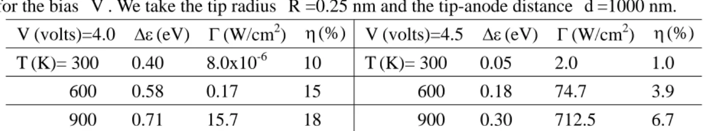
since Γ approaches Δε(j/e). Since Δε increases continuously with decreasing V, η can reach a very lar e value, say theg thermodynamic limit, for a very small V. By Eq. (5), Γ increases at the less rate that j as V increases. This means that η is small for large V even if Γ is large. It may be a drawback of field emission cooling that either Γ or η only can be large over the entire range of V. As mentioned above, however, there are two factors, T and R , to improve cooling. At high T , Γ and η c altogether be large. For small an R , η can become large since j is larg even for small e V. Niche values of Δε, Γ , and η ar shown in
ble 1. For V=4.0 volts, we obtain
e
Ta η=10 and 18
. The exact value of e
% at
e Fi
gion of
tips per centim T
g.
=300 and 900 K, respectively. For
d to be ider the V F = (or Spindt-type
4.5 volts, we have η =1.0 and 6.7 % at T =300 and 900 K, respectively.
To figure out the supposed cooler in more detail (s 1), we need to estimate Φ and I numerically with a certain choic
e
can not be determined since
) varies f n over the r em 16 If
take a reas ble v 24
h
e of
o
ich has an array of 10 A na A e j constant over j r A om cathode w
position to positio ission.
ter square and a current of 1 nA is assume
s alue of A . As a typical device, we con
9 , we can
per tip. This make it poss to consider (= ) in the range from 0.1 mA to 100 A . This will s find
I jA ible
make u A≈0.01 cm2. When the bias of V=4.5 volts is applied, we have Φ=ΓA≈ , 0.75 and 7.1 watts at T 600, and K, respectively. For V=5.0 volts, we hav
0 e
.02
=300, 900 Φ 2.3, ≈
21.6 and 80.3 watts at the same above temperatures, respectively. It looks hat the current obtained Nottingham effect is comparable to the Peltier effect.15,23 Ac ording to the situatio , either one may be more effective than the other in cooling an electronic device.
ACKNOWLEDGMENT
This research was supported by the Basic Science Research Program through National Research Foundation of Korea funded by the Ministry of Education, Science and Technology (Grant No. 2011-0009500). t ly c n 1 W 9 76, 4362 (1994).
balle, B. Y. M zhes, and T. W. Kenny, Appl. Phys. Lett. , 2572 (20
2 G. S. Nola id, J. Appl. Phys. 85, 4066 (1999).
r a K. K. Likharev, Appl. Phys. Lett. 75, 2491 (1999).
ler, B. L. Wei nd N. M. M ppl.
201 References
. Nottingham, Phys. Rev. 59, 907 (1941). 2
G. M. Fleming and J. E. Henderson, Phys. Rev. 58, 887 (1940). 3
F. M. Charbonnier, R. W. Strayer, L. W. Swanson, and E. E. Martin, Phys. Rev. Lett. 13, 397 (1964).
4
L. W. Swanson, L. C. Crouser, and F. M. Charbonnier, Phys. Rev. 151, 327 (1966 5
M. Drechsler, Z. Naturforsch. A 18, 1367 (1963). 6
I. Engle and P. H. Cutler, Surf. Sci. 12, 208 (1968). 7
T. S. Fisher and D. G. Walker, Trans. ASME vol. 124, 954 (2002). 8
T. L. Westover and T. S. Fisher, Heat Transfer Eng. 29, 395 (2008).
).
78
iskovsky, A G. D. Mahan, J. Appl. Phys.
otkov 1). 10 Y. Hishnuma, T. H. Ge oy 01). 11
A. Shakouri, C. LaBounty, J. Piprek, P. Abraham, and J. E. Bowers, Appl. Phys. Lett. 74, 88 (1999).
1 s and H. J. Goldsm nd
13. A. N. Ko 14
M. S. Chung, S. C. Hong, A. Mayer, P. H. Cut ss, a Phys. Lett. 92, 083505 (2008).
15
M. S. Chung, A. Mayer, B. L. Weiss, N. M. Miskovsky, and P. H. Cutler, Appl. Phys. Lett. 98, 243502 (
16
17
A. Modinos, Field, Thermionic, and Secondary Electron Emission Spectroscopy (Plenum,
t. 69, 2527 (1992). 1555 (1986).
nz, J. Kähler, A. Waag, and E. Peiner, J. Electronic Mater. 42, 2381 (2013).
n Physics vol. 83 (Academic New York, 1984).
18
T. T. Tsong, Surf. Sci. 81, 28 (1979). 19
Vu T. Binh, S. T. Purcell, N. Garcia, and J. Doglioni, Phys. Rev. Let 20
W. W. Lui and M. Fukuma, J. Appl. Phys. 60, 21
N. D. Arora, J. R. Hauser, and D. J. Roulston, IEEE Trans. Electron Devices vol. ED-29, 292 (1982).
22
O. Madelung, Semiconductors Basic Data, 2nd ed., (Springer, New York, 1996), p.200. 23
A. Stra 24
I. Brodie and C. A. Spindt, Vacuum Microelectronics, Advances i Press, New York, 1992), p.1.
Table 1. Cooling Characteristics. Cooling of field emission from the n-type Si tip is described by the energy exchange Δε, the power density Γ , and the efficiency η at temperature and for the bias . We take the tip radius
T
V R =0.25 nm and the tip-anode distance d=1000 nm.
V(volts)=4.0 Δε(eV) Γ (W/cm2) η(%) V(volts)=4.5 Δε(eV) Γ (W/cm2) η (%) T (K)= 300 0.40 8.0x10⁻⁶ 10 T (K)= 300 0.05 2.0 1.0
600 0.58 0.17 15 600 0.18 74.7 3.9
Figure Captions
Fig. 1 Schematic of a Supposed Field Emission Cooler. Energy exchange process takes place between the n-type semiconductor cathode and the conduction electron. The positive energy exchange cools down a sample at temperature T.
Fig. 2 Vacuum Potential Energy for a Spherical Cathode of N-Type Si. The potential falls down in a different way according to the bias (in volts) and the tip radius
U
V R (in nm).
Fig. 3 Plot of Current Density vs. Bias . The exhibits different Fowler-Nordheim plots according to the tip radius
j V j
R and temperature T . The effect of R results from the enhanced field and the modified barrier.
Fig. 4 Plots of Exchange Energy Δε vs. Bias V. We set the tip radius R =0.25 nm and the tip-anode distance d=1000 nm. The Δε increases with decreasing V and increasing T .
Fig. 5 Plots of Cooling Power Density Γ vs. Bias . The maximum cooling power increases rapidly with increasing but is located about =5.2 volts with a slight T-dependence.
V
replacement emission
e
V
anode
metal
e
sample T replacement emissione
V
V
anode
metal
metal
e
sample T Fig. 1 D istance x(nm ) -2 -1 0 1 2 3 4 5 6 7 8 9 Potential Energy U(eV) -1 0 1 2 3 EC n=1019cm-3 d=1000 nm R =0.5, V =4.0 EV R =inf., V =1000 R =2.0, V =4.0 R =0.25, V =4.0 Fig. 2Bias V(Volts) 4.0 4.5 5.0 5.5 En ergy Exch ange Δε (eV) 0.0 0.1 0.2 0.3 0.4 0.5 0.6 0.7 0.8 R=0.25nm d=1000nm Fig. 3 Fig. 4 Fig. 5 Bias V(Volts) 4.0 4.5 5.0 5.5 Cooling Power Γ (W/cm 2 ) 0 2000 4000 6000 8000 10000 R=0.25nm d=1000nm 300 K 600 K 800 K 900 K 300 K 600 K 800 K 900 K Bias V(volts) 10-3 10-2 10-1 100 101 102 103 104 105 106 107 4.0 4.5 5.0 5.5 6.0 d=1000 (nm) R=0.25 R=1.0 R=0.5 600K 300K Cu rre nt De ns ity j( A/c m 2 )