HAL Id: tel-00782328
https://tel.archives-ouvertes.fr/tel-00782328
Submitted on 29 Jan 2013
HAL is a multi-disciplinary open access archive for the deposit and dissemination of sci-entific research documents, whether they are
pub-L’archive ouverte pluridisciplinaire HAL, est destinée au dépôt et à la diffusion de documents scientifiques de niveau recherche, publiés ou non,
Tao Zhou
To cite this version:
Tao Zhou. Study of passive microwave and millimetre wave components based on matematerials and ferrite. Other. INSA de Lyon, 2012. English. �NNT : 2012ISAL0017�. �tel-00782328�
Présentée devant
L’institut national des sciences appliquées de Lyon
Pour obtenir le grade deDocteur
École doctorale: Electronique, Electrotechnique et Automatique Par
ZHOU Tao
Etude de composants passifs hyperfréquences
à base de métamatériaux et de ferrite
(Study of passive microwave and millimeter wave
components based on metamaterials and ferrite)
Soutenue le 6 Mars 2012 devant la Commission d’examen
Rapporteur FLECHET Bernard Professeur (Université de Savoie) Examinateur CALMON Francis Professeur (INSA de Lyon)
Rapporteur PARRA Thierry Professeur (Université Paul Sabatier) Examinateur GAUTIER Brice Professeur (INSA de Lyon)
Co-directeur de thèse VINCENT Didier Professeur (Telecom Saint-Etienne)
Directeur de thèse LE BERRE Martine Maître de conférences HdR (INSA de Lyon)
CHIMIE CHIMIE DE LYONhttp://www.edchimie-lyon.fr
Insa : R. GOURDON
M. Jean Marc LANCELIN
Université de Lyon – Collège Doctoral Bât ESCPE 43 bd du 11 novembre 1918 69622 VILLEURBANNE Cedex Tél : 04.72.43 13 95 [email protected] E.E.A. ELECTRONIQUE, ELECTROTECHNIQUE, AUTOMATIQUE http://edeea.ec-lyon.fr Secrétariat : M.C. HAVGOUDOUKIAN [email protected] M. Gérard SCORLETTI
Ecole Centrale de Lyon 36 avenue Guy de Collongue 69134 ECULLY Tél : 04.72.18 60 97 Fax : 04 78 43 37 17 [email protected] E2M2 EVOLUTION, ECOSYSTEME, MICROBIOLOGIE, MODELISATION http://e2m2.universite-lyon.fr Insa : H. CHARLES
Mme Gudrun BORNETTE
CNRS UMR 5023 LEHNA
Université Claude Bernard Lyon 1 Bât Forel 43 bd du 11 novembre 1918 69622 VILLEURBANNE Cédex Tél : 04.72.43.12.94 [email protected] EDISS INTERDISCIPLINAIRE SCIENCES-SANTE http://ww2.ibcp.fr/ediss Sec : Safia AIT CHALAL Insa : M. LAGARDE
M. Didier REVEL
Hôpital Louis Pradel Bâtiment Central 28 Avenue Doyen Lépine 69677 BRON Tél : 04.72.68 49 09 Fax :04 72 35 49 16 [email protected] INFOMATHS INFORMATIQUE ET MATHEMATIQUES http://infomaths.univ-lyon1.fr M. Johannes KELLENDONK
Université Claude Bernard Lyon 1 INFOMATHS Bâtiment Braconnier 43 bd du 11 novembre 1918 69622 VILLEURBANNE Cedex Tél : 04.72. 44.82.94 Fax 04 72 43 16 87 [email protected] Matériaux MATERIAUX DE LYON Secrétariat : M. LABOUNE PM : 71.70 –Fax : 87.12 Bat. Saint Exupéry [email protected]
M. Jean-Yves BUFFIERE
INSA de Lyon MATEIS
Bâtiment Saint Exupéry 7 avenue Jean Capelle 69621 VILLEURBANNE Cédex
Tél : 04.72.43 83 18 Fax 04 72 43 85 28 [email protected]
MEGA
MECANIQUE, ENERGETIQUE, GENIE CIVIL, ACOUSTIQUE
Secrétariat : M. LABOUNE PM : 71.70 –Fax : 87.12 Bat. Saint Exupéry [email protected]
M. Philippe BOISSE
INSA de Lyon Laboratoire LAMCOS Bâtiment Jacquard 25 bis avenue Jean Capelle 69621 VILLEURBANNE Cedex
Tél :04.72.43.71.70 Fax : 04 72 43 72 37 [email protected]
(UMR CNRS 5270), dont le directeur est Monsieur Guy Hollinger, elle a été di-rigé par Madame Martine LE BERRE et Monsieur Didier VINCENT. Je les re-mercie de m’avoir accueilli dans ce laboratoire et soutenu tout au long de mon travail.
Je voudrais remercier mon directeur de thèse, Madame Martine LE BERRE, Maître de conférences de l’INSA de LYON, pour m’avoir proposé ce sujet et pour avoir accepter de diriger ma thèse. Je la remercie d’avoir trouvé le temps, m’avoir conseillé et m’encouragé tout au long de mon travail. Je vou-drais qu’elle trouve ici toute l’expression de ma reconnaissance.
Je tiens aussi à remercier mon co-directeur de thèse, Monsieur Didier VINCENT, Professeur à l’université Jean Monnet de Saint-Etienne, pour son soutien et son suivi.
Je remercie tout particulièrement Monsieur Francis CALMON, Profes-seur de l’INSA de LYON, qui a cordialement accepté d’être membre du jury lors de ma thèse.
J’adresse toute ma reconnaissance à Monsieur Brice GAUTIER, Pro-fesseur de l’INSA de LYON, qui a cordialement accepté d’être membre du jury lors de ma thèse.
Un très grand merci à Monsieur Bernard FLECHET, Professeur de l’Université de Savoie, et à Monsieur PARRA Thierry, Professeur de l’Université Paul Sabatier, qui ont cordialement accepté d’être rapporteur de ce travail.
Je tiens également à remercier madame Béatrice Payet-Gervy, Maître de conférences à l’université Jean Monnet de Saint-Etienne, pour son aide dans la partie mesure de cette thèse.
J’ai une énorme pensée pour toute ma famille, mes parents, et mes frères, sans qui je n’en serais pas là aujourd’hui.
Enfin, je terminerais en remerciant tous mes collègues pour les bons moments que nous avons partagés : Wael HOURANI, Wei XUAN, Fengyuan SUN, Ahmed GHARBI, Sylvain PELLOQUIN, Jean-Etienne LORIVAL, Has-san CHAMAS, Antonin GRANDFOND, Guillaume HYVERT.
Contents
General introduction
1
Basic concepts
1.1 Introduction
1.2 Transmission line theory
1.2.1 Traditional reciprocal transmission line 1.2.2 Nonreciprocal transmission line
1.2.3 Transmission line network analysis
1.2.3.1 Impedance and admittance matrices 1.2.3.2 Transmission matrix [ABCD]
1.2.3.3 Scattering and transfer matrices
1.3 Coplanar waveguide
1.3.1 Conventional coplanar waveguide
1.3.1.1 CPW has infinite-width ground planes 1.3.1.2 CPW has finite-width ground planes 1.3.1.3 Consideration of conductor thickness 1.3.1.4 Attenuation constant
1.3.2 Conductor backed coplanar waveguide
1.4 Magnetic material
1.4.1 Diamagnetism 1.4.2 Paramagnetism
1.4.3 Ferromagnetism and Ferrimagnetism 1.4.4 Antiferromagnetism 1.4.5 Ferrites 1.5 Metamaterials 1.5.1 Definition of metamaterials 1.5.2 History of metamaterials 1.5.3 Applications of metamaterials
1.5.3.1 Guided wave applications 1.5.3.2 Radiated wave applications 1.5.3.3 Other applications of interest
1.6 Conclusion
1.7 Bibliography
2
Conventional coplanar
components on alumina
2.1 Introduction
2.2 Fabrication of coplanar components on alumina
2.2.1 Photolithography
2.2.2 Vacuum deposition / evaporation
2.3 Simulation and modelling
2.3.1 Finite element simulation 2.3.2 Modelling
2.3.2.1 Analytical modelling of CPW
2.3.2.2 Analytical modelling of gap capacitors
2.3.2.3 Analytical modelling of interdigital capacitors 2.3.2.4 Analytical modelling of shunt inductor
2.3.2.5 Calculation of capacitance and inductance from S parameters
2.4 Results of coplanar components on alumina
2.4.1 CPW on alumina
2.4.1.1 S parameters
2.4.1.2 Propagation constant 2.4.1.3 Change in reference planes 2.4.2 Coplanar gap capacitor
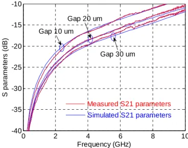
2.4.2.1 Measured and simulated S parameters 2.4.2.2 Values of capacitance
2.4.3 Coplanar interdigital capacitor
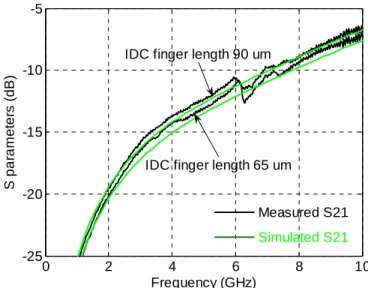
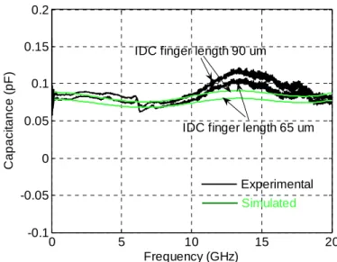
2.4.3.1 Measured and simulated S parameters 2.4.3.2 Values of capacitance
2.4.4 Coplanar shunt inductor
2.4.4.1 Measured and simulated S parameters 2.4.4.2 Values of inductance
2.6 Bibliography
3
Coplanar components on ferrite
3.1 Introduction
3.2 Ferrite material
3.2.1 Spinel 3.2.2 Garnet 3.2.3 Hexaferrite
3.3 Fabrication of coplanar components on YIG
3.3.1 Polish of film
3.3.2 Fabrication of component
3.4 Modelling, simulation, and calculation
3.4.1 Modelling of ferrite material 3.4.2 Simulation
3.4.3 Calculation of propagation constant
3.5 Coplanar component on substrate ferrite
3.5.1 CPW on substrate BaM
3.5.1.1 Applied field out of the plane of CPW – filter 3.5.1.2 Applied field in the plane of CPW – isolator 3.5.2 CPW on YIG without applied Field
3.5.2.1 S parameters
3.5.2.2 Propagation constant
3.5.3 CPW on YIG with applied field in the plane of CPW 3.5.3.1 S parameters
3.5.3.2 Propagation constant 3.5.4 Coplanar gap capacitor on YIG
3.5.4.1 Measured and simulated S parameters 3.5.4.2 Values of capacitors
3.5.5 Coplanar inter-digital capacitor on YIG
3.5.5.1 Measured and calculated S parameters 3.5.5.2 Values of capacitors
3.5.6 Coplanar inductor on YIG
3.7 Bibliography
4
Coplanar composite
right/left-handed metamaterials
4.1 Introduction
4.2 Modelling, simulation, and calculation
4.2.1 Transmission line approach of metamaterials 4.2.2 Simulation and calculation
4.2.3 Example
4.3 CRLH metamaterials on alumina
4.3.1 Equivalent circuits
4.3.2 Measured and simulated S parameters 4.3.3 Propagation constants
4.4 CRLH metamaterials on YIG without applied field
4.4.1 Equivalent circuits 4.4.2 Measured S parameters 4.4.3 Propagation constants
4.5 CRLH metamaterials on YIG with applied field
4.5.1 Measured S parameters 4.5.2 Propagation constants 4.6 Conclusion 4.7 Bibliography General conclusion List of publications
General introduction
This thesis concerns passive microwave and millimeter wave components based on ferrites and metamaterials. The main objective of this work is to study the physical properties of combined left-handed transmission lines associated with negative permeability ferrite. The modelling, fabrication and characterization of components have been achieved in collaboration between the INL and LT2C.
As a coplanar transmission line, coplanar waveguide (CPW) offers several attractive features, it is very suitable for microwave and millimeter wave components. The CPW can be easily use to integrate some basic lumped elements such as coplanar capacitors and shunt inductors, which can be easily applied to build composite right/left-handed transmission lines, filters, resona-tors... The properties of CRLH TL which consist of distributed structures with lumped components will be studied in this thesis: the equivalent circuits, the S parameters, the propagation constants.
Since the first microwave ferrite device was proposed in 1949, the fer-rite materials have been applied to many microwave components such as isola-tors, circulaisola-tors, phase shifters, and filters. The development of ferrite compo-nents was strongly related to the knowledge of spin interaction in ferrite materials. The ferrite materials are so important that, for some purposes, we can not find an alternative semiconductor device that satisfies similar requirements.
In the past 10 years, there has been a great deal of interest in the com-posite right/left-handed (CRLH) transmission lines (TLs) metamaterials (MTMs), which introduced by Caloz et al. and other groups. The CRLH TLs can be realized by using traditional right-handed (RH) TLs loaded with series capacitors (IDCs) and shunt inductors. Novel microwave applications like guided wave application and radiated wave application can be realized by using the unique features of MTMs, they exhibit new performance compared with similar classical devices, these novel CRLH components are couplers, zeroth order resonators, zeroth order antennas, leaky-wave antenna, filters etc.
In this thesis we propose several coplanar components based on metamaterials, with which we can get a novel property “left-handed” or “CRLH”. When the CRLH TLs are integrated with substrate ferrites, we expected a new property which combines the “CRLH” property and nonreciprocity together. We can get nonreciprocity by modeling the ferrite substrate, and “left-handed” property by modeling the structure of CRLH.
This manuscript contains four chapters. The first chapter of this manu-script will focus on theories of microwave transmission lines, coplanar waveguides, magnetic materials and general concepts about metamaterials. We will begin with the theories of traditional transmission lines and nonreciprocal transmission lines, and then we will present the analysis of transmission lines,
methods of calculation of the parameters characterizing wave propagation (ma-trix [Z] ma(ma-trix [Y], ma(ma-trix [ABCD] and ma(ma-trix [S]). The classsification of mag-netic materials will be presented in different groups. Finally, we will introduce metamaterials. The definition, history, and some applications of metamaterials in microwave and millimetre wave will be indicated.
In the second chapter, we will present the conventional coplanar components on alumina substrate. We will start with the fabrication of components. Then we will simulate and modelize coplanar waveguides, capacitors, and inductors. Finally, we will discuss the calculated results, the simulated and measured CPW, capacitances, and inductances, we will compare the results.
In the third chapter, we focus on coplanar components on ferrite substrate. We will discuss the important characteristics of ferrite materials classified into different groups depending on their properties, and the main characteristics of ferrites used in this work. We will present the process of fabrication of components when it differs from the one on alumina. Then we will show simulations and modeling of coplanar waveguide on ferrite, coplanar capacitances and the behavior due to coplanar inductances on ferrite.
The fourth chapter is devoted to metamaterials based on the CRLH TL. This type of TL allows a negative phase velocity in a certain frequency band. We will make the modeling, 3D simulations, and parameter extraction of the CRLH metamaterial. Then we will presente the CRLH TL on alumina and on YIG (with field and without applied field). The variations of the experimental and simulated parameters S, the propagation constants β as a function of frequency are presented.
1
Basic concepts
1.1 IntroductionMicrowaves are electromagnetic waves with frequencies ranging from 300 MHz to 300 GHz (wavelengths: 1 m to 1 mm) [1]. This definition includes ultra high frequency (300 MHz-3 GHz, or 1 to 0.1m) [2], Super high frequency (3GHz-30 GHz, or 10cm to 1 cm) [3], and extremely high frequency (30 GHz-300GHz, or 10mm to 1mm) [4]. With RF engineering, the band from 300 MHz to 30 GHz is typically considered to be “microwaves”, the frequency band above 30 GHz is considered to be “millimetre waves”[2,4].
The tremendous growth in mobile communications during the past 20 years has caused a great increase in the need for microwave and millimetre wave components. Besides this, microwave and millimetre wave components are widely used in application areas, such as radar and navigation systems, sat-ellite communication networks, remote sensing, and industrial measure-ments [5]. Microwave and millimetre wave components are becoming more available and affordable because of advances in the design, processing, testing, and packaging technology. There exist a lot of microwave and millimetre-wave components, for example, coplanar waveguides (CPWs) [6-14], metamaterials (MTMs) [15-22], components based on ferrite materials [1-3], as will be intro-duced in the coming chapter.
1.2 Transmission line theory
Transmission line (TL) is widely used in radio-frequency domains, the TL is a special cable designed to carry electromagnetic signals [1-10]. There are many types of TL such as coaxial cable [1-3], microstrip line [10], stripline [10] and wageguide [1-2]. The CPW [6-7] will be discussed in Chapter 2 and Chapter 3.
1.2.1 Conventional reciprocal TL
The TL theory bridges the gap between field analysis and circuit theory, it is very important in microwave and millimetre wave network analysis [1]. The wave propagate along the TL can be approached from a specialization of Max-well’s equations or from an extension of circuit theory.
The key difference between the TL theory and the circuit theory is the electrical length. The physical length of a TL network may be a considerable fraction of a wavelength, or many wavelengths, while the circuit theory as-sumes that the physical length of a network is much smaller than the electrical
wavelength. The circuit theory is a lumped element network, while the TL is a distributed element network.
Figure 1.1 Transmission line
Figure 1.2 Equivalent circuit of TL
The TL is shown in Figure 1. 1, it’s composed of 2-wire line, and since TL (for TEM propagation) wave propagation has at least 2 conductors [1]. The short line length ∆zof TL can be modelled as a lumped element circuit consists of R, L, C and G, as shown in Figure 1.2.
where,
R is series resistance per unit length, inΩ/m, represents the resistance due to the finite conductivity of the 2 lines.
L is series inductance per unit length, inH /m, represents the self-inductance of the 2 lines.
C is shunt capacitance per unit length, in S /m, represents the capaci-tance due to the close proximity of the 2 lines.
G is shunt conductance per unit length, inF /m, represents the con-ductance due to the dielectric loss in the material between the 2 lines.
From the equivalent circuit of TL, for finding the voltage and current on the TL, Kirchhoff’s voltage law (KVL) and Kirchhoff’s current law (KCL) can be applied to get:
t t z i z L t z i z R t z v t z z v ∂ ∂ ∆ − ∆ − = ∆ + , ) ( , ) ( , ) ( , ) ( (1.1) t t z z i z C t z z v z G t z i t z z i ∂ ∆ + ∂ ∆ − ∆ + ∆ − = ∆ + , ) ( , ) ( , ) ( , ) ( (1.2)
Dividing the 2 equations by ∆z(∆z 0), the telegrapher equations-time domain form of TL are given:
) , ( ) , ( ) , ( ) , ( ) , ( ) , ( t z Li j t z i R t t z i L t z i R z t z v t z z v =− −
ω
∂ ∂ − − = ∆ − ∆ + (1.3) z i(z,t) + - v(z,t) i(z+∆z,t) v(z+∆z,t) ZC ∆z Port 2 Port 1 L∆z C∆z G∆z i(z,t) + - v(z,t) i(z+∆z,t) v(z+∆z,t) + - ∆z R∆z) , ( ) , ( ) , ( ) , ( ) , ( ) , ( t z Cv j t z v G t t z v C t z v G z t z i t z z i
ω
− − = ∂ ∂ − − = ∆ − ∆ + (1.4) For the sinusoidal steady-state condition (cosine-based phases), the 2 equations can be simplified as:) ( ) ( ) ( ) ( z ZI z I L j R dz z dV =− +
ω
=− (1.5) ) ( ) ( ) ( ) ( z YV z V C j G dz z dI =− +ω
=− (1.6) where Z and Y are the series impedance and shunt admittance per unit length.The 2 equations can be solved simultaneously to give wave equations of V(z)and I(z)
0
)
(
)
(
2 2 2=
−
V
z
dzz
V
d
γ
(1.7)0
)
(
)
(
2 2 2=
−
I
z
dzz
I
d
γ
(1.8) where the complex propagation constant)
)(
(
R
j
L
G
j
C
ZY
j
β
ω
ω
α
γ
=
+
=
=
+
+
(1.9) Travelling wave solutions to wave equations ofV
(z
)
andI
(z
)
z z e V e V z V( )= 0+ −γ + 0− γ (1.10) z z e I e I z I( )= 0+ −γ + 0− γ (1.11) WhereV0+, − 0 V , I0+ and − 0
I are unknown amplitudes of voltage and cur-rent waves of port 1 and port 2, the e−γzand eγz represents wave propagation in the +z direction, and wave propagation in the-z direction, respectively.
Applying Equation 1.5 to the equation 1.11 given ) ( ) ( V0 e z V0 ez L j R z I γ γ
ω
γ
+ − − − + = (1.12) Dividing the Equation 1.10 and Equation 1.11 with the equation 1.12, the characteristic impedance ZCis given:C j G L j R L j R ZC
ω
ω
γ
ω
+ + = + = (1.13) C Z Y Z I V I V = = = −− + + 0 0 0 0 (1.14) The wavelength of TL isβ
π
λ
g = 2 (1.15) The phase velocityf t z V g t p
λ
β
ω
= = ∆ ∆ = ∆ 0 lim f (1.16) The group velocityω
ω
ω
β
d
dV
v
V
d
d
V
p g p g−
=
=
−1
1 (1.17)For a TL with infinite conductor conductivity (
σ
∞), zero dielectric conductivity (σ
0) and no radiation loss, the loss of TL is very small and can be neglected, the circuit components (R and G) which represent loss become ze-ro, R=G=0The corresponding propagation constant can be simplified as
LC
j
C
j
G
L
j
R
j
β
ω
ω
ω
α
γ
=
+
=
(
+
)(
+
)
=
(1.18) where the attenuation constantα
=0,β
=ω
LCThe characteristic impedance of TL is a real number
C
L
Z
C=
(1.19) The wavelength of lossless TLLC g
ω
π
β
π
λ
= 2 = 2 (1.20) The phase velocityLC Vp = = 1
β
ω
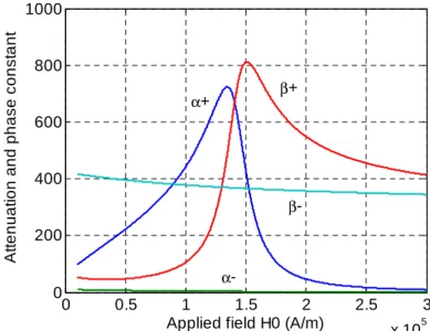
(1.21) 1.2.2 Novel nonreciprocal TLNon reciprocal isotropic medium was first introduced by Tellegen in 1948 [23]. The realization of the gyrator by a new medium, which obtained by imbedding permanent electric and magnetic dipoles in a host medium, was discussed by him. The plane wave propagation in such medium was presented by Chambers in 1956 [24]. The theory of nonreciprocal and no symmetrical uniform TLs was proposed by Ismo Lindell in 1992 [25].
Figure 1.3 The equivalent circuit of a nonreciprocal TL
a+jb L C a+jb I(z) + - v(z) I’(z) V’(z) + -
The equivalent circuit of a nonreciprocal TL is shown in Figure 1.3. Like the previous reciprocal TL, L is the distributed series inductance per unit length, C is the distributed capacitance per unit length, a and b are 2 new pa-rameters of TL (similar to L and C), a is due to chirality, b is due to non-reciprocity. A voltage-controlled voltage source and a current-controlled cur-rent source are added to the equivalent circuit of conventional reciprocal TL.
The impedances and admittances of this TL can be written as:
L j Z=
ω
(1.22) ) ( ' j a jb Z =ω
− (1.23) C j Y =ω
(1.24) ) ( ' j a jb Y =ω
+ (1.25) The 2 new parameters a and b of TL can be written as:LC k
a= r (1.26)
LC
b=
χ
r (1.27) wherek
ris the relative chirality parameter, which corresponds to non-reciprocity on transmission in circuit theory,χ
ris the relative Tellegen parame-ter, which corresponds to non reciprocity in electromagnetic theory. the pa-rameter b can also be presented in terms of an angleθ
:LC
b=sin
θ
(1.28) The voltage and current relationships between 2 ports are:) ( ) ( ) ( ) ( ' z j a jbV z j LI z V =−
ω
− −ω
(1.29) ) ( ) ( ) ( ) ( ' z j CV z j a jb I z I =−ω
−ω
+ (1.30) Solve the engine value problem of the above wave equations, we get:V LI V jb a
ω
γ
ω
( − ) + = (1.31) I I jb a CVω
γ
ω
+ ( + ) = (1.32) Travelling wave solutions to wave equations of V(z)and I(z)z z e V e V z V( )= 0+ −γ+, + 0− γ−, (1.33) z z e I e I z I 0 , , 0 ) ( = + −γ+ + − γ− (1.34) where
(
r kr)
(
kr)
a b LC− + = − + = + = +ω
ω
γ
χ
γ
θ
γ
2 0 1 2 0 cos (1.35)(
r kr)
(
kr)
a b LC− − = − − = − = −ω
ω
γ
χ
γ
θ
γ
2 0 1 2 0 cos (1.36)LC
ω
γ
0=
(1.37)The characteristic impedances
)
(
)
(
jb
a
L
C
jb
a
Z
−
−
=
+
−
=
+ + +ω
γ
ω
ω
ω
γ
(1.38))
(
)
(
jb
a
L
C
jb
a
Z
−
+
=
+
+
=
− − −ω
γ
ω
ω
ω
γ
(1.39) The above formulas can also be written:θ j Ce Z c b j C b C L Z+ = − 2 − = − 2 (1.40) θ j Ce Z c b j C b C L Z− = − 2 + = + 2 (1.41) C L Y Z C C = = 1 (1.42) The characteristic admittances:
θ j Ce Y Y+ = + (1.43) θ j Ce Y Y− = − (1.44) It is indicated that, the propagation constant
γ
± depend on the parame-ter a (k
r), the impedance±
Z and admittance Y± depend on the parameter b (
χ
r).1.2.3 Transmission line network analysis
1.2.3.1 Impedance and admittance matrices
The impedance matrix [Z] and admittance matrix [Y] are defined by the termi-nal/port voltages and currents of networks [1-3], as shown in Figure 1.4. The 2 ports in the figure can be any TL mode.
Figure 1.4 2-port network
The relationships of voltages and currents of the network between port 1 and port 2: 2 12 1 11 1
Z
I
Z
I
V
=
+
(1.45) 2 22 1 21 2Z
I
Z
I
V
=
+
(1.46) Its matrix form
=
2 1 22 21 12 11 2 1I
I
Z
Z
Z
Z
V
V
(1.47) Similarly, the admittance matrix [Y] can be obtained:2 12 1 11 1
Y
V
Y
V
I
=
+
(1.48) 2 22 1 21 2Y
V
Y
V
I
=
+
(1.49) [ Z ] I1 V1 + - I2 V2 + -Its matrix form
=
2 1 22 21 12 11 2 1V
V
Y
Y
Y
Y
I
I
(1.50) From the above equations, we can see that both [Z] matrix and [Y] ma-trix relate the port voltages and currents, and are the inverses of each other1
] [ ]
[Z = Y − (1.51) The impedance parameters can be obtained as:
0 2 1 1 1 1 =
=
II
V
Z
, looking in input impedance of port 1, when port 2 open ended0 1 2 1 2 1 =
=
II
V
Z
, transfer impedance between port 1 to port 2, when port 1 open ended 0 2 1 2 1 2 ==
II
V
Z
, transfer impedance between port 2 to port 1, when port 2 open ended 0 1 2 2 2 2 ==
II
V
Z
, looking in input impedance of port 2, when port 1 open ended Similarly, we can find the admittance parameters as:0 2 1 1 1 1 =
=
VV
I
Y
, looking in input admittance of port 1, when port 2 short ended0 1 2 1 2 1 =
=
VV
I
Y
, transfer admittance between port 1 to port 2, when port 1 short ended 0 2 1 2 1 2 ==
VV
I
Y
, transfer admittance between port 2 to port 1, when port 2 short ended 0 1 2 2 2 2 ==
VV
I
Y
, looking in input admittance of port 2, when port 1 short ended If the network is lossless, the [Z] parameters and [Y] parameters are purely imaginary, if the network is lossy, The [Z] parameters and [Y] parame-ters are complex.If the network is reciprocal, The [Z] parameters and [Y] parameters are symmetric,
Z
The nonreciprocal network is shown in Figure 1.5.
Figure 1.5 The nonreciprocal network
At point z1 of network 1 , 1 , ) 1 (z V e j Z V ej Z V = + −γ+ + − γ− (1.53) 1 , 1 , ) 1 (z Y V e j Z Y V ej Z I = + + − γ+ − − − γ− (1.54) At point z1 of network 2 , 2 , ) 2 (z V e j Z V ej Z V = + − γ+ + − γ− (1.55) 2 , 2 , ) 2 (z Y V e j Z Y V ej Z I = + + −γ+ − − − γ− (1.56) where
(
r kr)
(
kr)
a b LC− + = − + = + = +ω
ω
γ
χ
λ
θ
γ
2 0 1 2 0 cos (1.57)(
r kr)
(
kr)
a b LC− − = − − = − = −ω
ω
γ
χ
λ
θ
γ
2 0 1 2 0 cos (1.58)LC
ω
γ
0=
(1.59)Assume z2 > z1, the impedance matrix is found
=
) 2 ( ) 1 ( 22 21 12 11 ) 2 ( ) 1 ( z I z I Z Z Z Z z V z V (1.60) where ) cos sin( ) cos cos( 11 0 0θ
γ
θ
θ
γ
t t jZc Z =− − (1.61) ) cos sin( cos 12 0 0θ
γ
θ
γ t e jZc Z t jkr − = (1.62) ) cos sin( cos 21 0 0θ
γ
θ
γ t e jZc Z t jkr − − = (1.63) ) cos sin( ) cos cos( 22 0 0θ
γ
θ
θ
γ
t t jZc Z =− + (1.64) C L Y Z C C = = 1 (1.65) 1 2 z z t= − (1.66) Lossless nonreciprocal network,11 11* Z Z =− (1.67) 22 22* Z Z =− (1.68) z I(z1) V+ V- V(z1 ) Port 1 z1 z2 V(z2 ) I(z2)
21 12* Z Z =− (1.69) 12 21* Z Z =− (1.70) 2
]
[
Z
=
Zc
] (1.71) The non-symmetry of network22 11 Z
Z ≠ (1.72) The non-reciprocity of network
21 12 Z
Z ≠ (1.73)
1.2.3.2 The transmission matrix (ABCD)
The ABCD parameters are defined by the terminal/port voltages and currents of networks [1-3], as shown in Figure 1.6; it’s quite convenient to obtain the ABCD matrix of cascaded networks.
Figure 1.6 2-port network with ABCD matrix
The relations of voltages and currents between port 1 and port 2:
2 2 1 AV B I V = + (1.74) 2 2 1 CV D I I = + (1.75) Its matrix form
=
2 2 1 1I
V
D
C
B
A
I
V
(1.76) For a cascade network shown in Figure 1.7
=
=
3 3 2 2 2 2 1 1 1 1 2 2 1 1 1 1 1 1I
V
D
C
B
A
D
C
B
A
I
V
D
C
B
A
I
V
(1.77) It is found that the overall [ABCD] matrix of a cascaded network can be easily evaluated by multiplying the ABCD matrix of each individual net-work:[
]
⋅⋅
⋅⋅
⋅⋅
=
n n n n nD
C
B
A
D
C
B
A
D
C
B
A
ABCD
2 2 2 2 1 1 1 1 (1.78) where N is the number of cascaded network.[ A B C D ] V1 + - I2 V2 + - I1 Port 1 Port 2
Figure 1.7 2-port cascade network
The ABCD parameters can be found as:
0 2 2 1 =
=
IV
V
A
, the voltage ratio of port 1 and port2, when port 2 is open ended.0 2 2 1 =
=
VI
V
B
, the transferring impedance from port 1 to port2, when port 2 is short ended. 0 2 2 1 ==
IV
I
C
, the transferring admittance from port 2 to port 1, when port 2 is open ended. 0 2 2 1 ==
VI
I
D
, the current ratio of port 1 and port 2, when port 2 is short ended. The relationships between ABCD parameters and impedance parame-ters
−
=
22 21 12 22 11 11 211
1
Z
Z
Z
Z
Z
Z
Z
D
C
B
A
(1.79) Network [ABCD]
1 0 1 Z
1 0 1 Y
l l jY l jZ lγ
γ
γ
γ
cos sin sin cos
+
+
+
+
3 3 1 3 3 2 3 1 2 1 3 3 3 2)
(
)
(
1
)
(
Y
Y
Y
Y
Y
Y
Y
Y
Y
Y
Y
Y
Y
Y
Z l Y Z Y3 Y1 Y2 [ A1 B1 C1 D1] V1 + - I2 I1 Port 1 V2 [ A2 B2 C2 D2] + - I3 V3 + - Port 2
+
+
+
+
3 3 2 3 3 3 2 3 1 2 1 3 3 1)
(
1
)
(
)
(
Z
Z
Z
Z
Z
Z
Z
Z
Z
Z
Z
Z
Z
Z
Table 1.1 The ABCD parameters of some 2-port network
1.2.3.3 Scattering parameters and transfer parameters
A) Scattering parameters
Scattering parameters (S parameters) are the most frequently used in RF engi-neering, for their derivation is based on forward and backward-travelling waves. The S parameters are defined by incident waves and reflected waves on TL networks [9]. A 2-port network is shown in Figure 1.8, the voltage waves on the terminals are used to define the S parameters of the network.
Figure 1.8 S parameters of 2-port network
Assume that the voltages and currents stimulated in ports, as shown in the figure. According to the TL theory, the port voltages and currents can be decomposed into backward travelling and forward travelling waves propagating on the transmission connected to the network:
− + + = 1 1 1 V V V (1.80) ) ( 1 1 1 1 − + − = V V Z I C (1.81) − + + = 2 2 2 V V V (1.82) ) ( 1 2 2 2 − + − = V V Z I C (1.83) where ZCis the characteristic impedance of the TL connected to the network.
The forward and backward travelling voltage waves can be determined by the solutions of the above equations:
2 1 1 1 I Z V V+ = + C (1.84) Z3 Z1 Z2 Network [ S ] a1 b1 I1 V1 + - I2 b2 a2 V2 + -
2 1 1 1 I Z V V− = − C (1.85) 2 2 2 2 I Z V V+ = + C (1.86) 2 2 2 2 I Z V V− = − C (1.87) The incident and reflected voltages on 2 ports of the network are nor-malized by the characteristic impedanceZC.
C
Z
V
a
+=
1 1 (1.88) CZ
V
a
+=
2 2 (1.89) CZ
V
b
−=
1 1 (1.90) CZ
V
b
−=
2 2 (1.91)The normalized voltages and currents of the 2 ports
1 1 1 1 1
a
b
Z
V
V
u
C+
=
+
=
+ − (1.92) 1 1 1 1 1)
(
b
a
Z
V
V
i
C−
=
−
=
+ − (1.93) 2 2 2 2 2a
b
Z
V
V
u
C+
=
+
=
+ − (1.94) 2 2 2 2 2)
(
b
a
Z
V
V
i
C−
=
−
=
+ − (1.95) The incident and reflected powers can be describe by incident and re-flected waves: 2 1 1 2 1 a P+ = (1.96) 2 1 1 2 1 b P− = (1.97) 2 2 2 2 1 a P+ = (1.98) 2 2 2 2 1 b P− = (1.99) The S parameters can be defined as the following form:2 12 1 11 1 S a S a b = + (1.100) 2 22 1 21 2 S a S a b = + (1.101) The matrix form of the above equations
=
2 1 22 21 12 11 2 1a
a
S
S
S
S
b
b
(1.102) The physical significance of S parameters:0 1 1 11 2= = a a b
S , represents the reflectance of port 1, when port 2 well matched, 0 1 2 21 2= = a a b
S , represents the transmission coefficient from port 1 to port 2, when port 2 well matched,
0 2 1 12 1= = a a b
S , represents the transmission coefficient from port 2 to port 1, when port 1 well matched,
0 2 2 22 1= = a a b
S , represents the reflectance of port 2, when port 1 well matched。
The relationships between S parameters and transmission parameters ABCD: D C B A D C B A S + + + − − + = 11 (1.103) D C B A BC AD S + + + − = 2( ) 12 (1.104) D C B A S + + + = 2 21 (1.105) D C B A D C B A S + + + + − + − = 22 (1.106) B) Transfer parameters
One disadvantage of the S parameters is that it’s difficult to get the S parame-ters of cascade networks, while it’s quite convenient to obtain the transfer ma-trix [T] of cascaded networks [9]. The overall T parameters of cascade networks can be obtained by multiplying the T parameters of each individual network.
Figure 1.9 Tranfer parameters of 2-port network
The T parameters can be defined
=
2 2 22 21 12 11 1 1b
a
T
T
T
T
b
a
(1.107) The T parameters of a cascade n network are[ ]
⋅⋅
⋅⋅
⋅⋅
=
+ + n n n n n n n n nT
T
T
T
T
T
T
T
T
T
T
T
T
, , 1 1 , , 33 32 23 22 22 21 12 11 (1.108) The relationships between T parameters and S parameters are
− − =
21 22 11 21 12 21 11 21 22 21 22 21 12 11 1 S S S S S S S S S S T T T T (1.109)
− − − =
11 12 11 21 22 11 21 12 11 21 22 21 12 11 1 T T T S T T T T T T S S S S (1.110)For getting the S parameters of a 2 port cascade networks, the S pa-rameters of each individual network can be converted to T papa-rameters. Then, the overall T parameters of the cascade networks can be find easily. Finally, the S parameters can be evaluated by the overall T parameters.
1.3 Coplanar waveguide
Coplanar waveguide (CPW) was first demonstrated by C.P.Wen [6] in 1969, since then it was widely used in microwave and millimetre wave integrated components [7,15]. The CPW is a type of planar TL, which fabricated on a di-electric substrate. A conventional CPW consists of centre strip conductor and 2 ground planes on dielectric substrate is shown in Figure 1.10.
The CPW supports a quasi-TEM mode of propagation; it offers several attractive features, such as uniplanar construction, easy integration, simple fab-rication, low dispersion, size reduction without limit and radiation loss reduc-tion. A ground plane exists between any two adjacent lines, hence it has a week cross talk effects between adjacent lines. The characteristic impedance is de-termined by the ratio of W/(W+2G), so the size reduction is possible without
[ T ] a1 b1 I1 V1 + - I2 b2 a2 V2 + -
limit, the only disadvantage being higher losses. The circuits using CPWs can be produced denser than microstrip circuits, which make CPW ideally suited for microwave and millimeter wave integrated components applications.
Figure 1.10 Conventional CPW on dielectric substrate: W-center conductor width,
G-slot width, h-substrate height, t-conductor thickness, L-physical length.
The CPWs can be usually classified as conventional CPW and conduc-tor backed CPW. For the conventional CPW, the ground planes are extended semi-infinitely on either side. However, in a practical conventional CPW the ground planes are extended finitely. For the conductor-backed CPW, a ground plane is added at the bottom surface of the substrate. A conductor backed CPW is shown in Figure 1.12.
1.3.1 Conventional CPW
For the conventional CPWs, the closed-form expressions of the effective dielec-tric constant and characteristic impedance with zero conductor thickness can be derived by using conformal-mapping methods [7], which are shown below
)
'
(
)
(
)
(
)
'
(
2
1
1
1 1k
K
k
K
k
K
k
K
r eff•
•
−
+
=
ε
ε
(1.111))
(
)
'
(
30
0k
K
k
K
Z
eff•
=
ε
π
(1.112) K represents the complete integral of the first kind, its values can be obtained by an integral or tabulated table. The corresponding K(k)/K(k') val-ues can be calculated by equations giving below:
≤ ≤ − + ≤ ≤ − + = 1 707 . 0 , ) ' 1 ) ' 1 ( 2 ln( 707 . 0 0 , ) ' 1 ) ' 1 ( 2 ln( ) ' ( ) ( k k k k k k k K k Kπ
π
(1.113) G W G t h Substrate Conduct x y z L1.3.1.1 CPW has infinite-width ground planes ) 2 /(W G W k = + (1.114) 2
1
'
k
k
=
−
(1.115) ) 4 / ) 2 ( sinh( ) 4 / sinh( 1 h G W h W k + =π
π
(1.116) 2 1 1' 1 k k = − (1.117)1.3.1.2 CPW has finite-width ground planes (width S)
(
) (
)
(
)
2 2 2 2 2 2 1 2 2 2 1 ) 2 ( W W G S S G W G W G W W k + + − + + + − + = (1.118) 21
'
k
k
=
−
(1.119) 2 1 1' 1 k k = − (1.120))
4
/
)
2
2
(
(
sinh
/
)
4
/
(
sinh
1
)
4
/
)
2
2
(
(
sinh
/
)
4
/
)
2
(
(
sinh
1
)
4
/
)
2
(
sinh(
)
4
/
sinh(
2 2 2 2 1h
S
G
W
h
W
h
S
G
W
h
G
W
h
G
W
h
W
k
+
+
−
+
+
+
−
⋅
+
=
π
π
π
π
π
π
(1.121)1.3.1.3 Consideration of conductor thickness t
When the conductor thickness t is considered, the effective width of center con-ductor increases and the effective slot width decrease. The corresponding effec-tive dielectric constant and characteristic impedance can be derived by formulas given below: G t k K k K G t t eff eff eff 7 . 0 ) ( ) ' ( ) 1 ( 7 . 0 ) ( + − − =
ε
ε
ε
(1.122) ) ( ) ' ( ) ( 30 0 e e eff K k k K t Z = ⋅ε
π
(1.123) where e e e eG
W
S
k
2
+
=
(1.124) 21
e ek
k
=
−
(1.125)∆ + =W We (1.126) ∆ − =G Ge (1.127)
+ = ∆ t a tπ
π
8 ln 1 25 . 1 (1.128) 1.3.1.4 Attenuation constantThe conductor attenuation constant and the dielectric attenuation constant for the conventional CPW with conductor thickness t can be evaluated from:
+ − + + + × + × = 0 2 2 4 ) 4 ln 1 ( 25 . 1 2 25 . 1 1 ) 4 ln( 25 . 1 10 88 . 4 t W G t G W W t t W t G G W P Z Rs eff c π π π π π ε π α (dB/m) (1.129) where
≤ ≤ − ≤ ≤
− = 1 707 . 0 , ) 1 ( 1 707 . 0 0 , ) ' ( ) ( ) ' )( ' 1 ( 2 2 3 k k k k k K k K k k k P (1.130)δ
ωµ
0 2 = sR is the surface resistivity of the conductor
δ
is the conductivity 0 ) 1 ( tan ) 1 ( 3 . 27λ
ε
ε
δ
ε
ε
α
− − = r eff eff r d (dB/m) (1.131) 0λ
is the free space wave length These equations are valid forW
t<< , h<<G
For a conventional CPW with thin dielectric, the radiation lose is [8]
g r r
Q
λ
π
α
=
(1.132) gλ
is the guided wave length, eff eff g f cε
λ
ε
λ
= = 0 (1.133) oc sc r r G k h k K k K Qψ
ψ
ε
ψ
( , , , ) ) ' ( ) ( 0 = (1.134) ] ) ( ) 1 ( 1 [ ] 4 ) ( ) 1 ( 1 [ ) )( ( ] 2 ) ( ) 1 ( 1 )[ 1 ( ) , , , ( 2 0 2 2 0 2 2 0 0 2 0 2 0 h k h k b k h k h k G k h r eff r r r r − + − + • − + − = ε ε ε ε ε ε ψ (1.135)eff r eff r sc h k h k
ε
ε
ε
ε
π
π
ψ
4 ) ( ) 1 ( 1 3 ] 4 ) ( ) 1 ( 1 )[ 8 1 ( 1 8 5 2 0 2 2 0 2 2 − + • − + − + = (1.136) eff r oc h kε
ε
π
π
ψ
4 ] ) ( ) 1 ( 1 )[ 8 1 ( 3 8 2 0 2 2 − + − + = (1.137) 1.3.2 Conductor backed CPWsFigure 1.11 Conductor backed CPW on dielectric substrate: W-center conductor width,
G-slot width, h-substrate height, t-conductor thickness, L-physical length.
For the conductor backed CPWs, the effective dielectric constant and character-istic impedance can be derived from equations given below
) ' ( ) ( ) ( ) ' ( 1 ) ' ( ) ( ) ( ) ' ( 1 1 1 1 1 k K k K k K k K k K k K k K k K r eff • + • • + =
ε
ε
(1.138) ) ' ( ) ( ) ' ( ) ( 1 60 1 1 0 k K k K k K k K Z eff + • =ε
π
(1.139) where ) 2 /(W G W k = + (1.140) 21
'
k
k
=
−
(1.141) ) 4 / ) 2 ( tanh( ) 4 / tanh( 1 h G W h W k + =π
π
(1.142) 2 1 1' 1 k k = − (1.143) G W G t h Substrate Conductor x y z L1.4 Magnetic materials
In a 4th century BC book “the Devil Valley Master (鬼谷 子)”, magnetic
materi-als have been described as: “The lodestone makes iron come or it attracts it”
[30]. In 380 BC, Plato wrote “stone which Euripides calls a magnet”. The stones mentioned above are actually magnetite (Fe3O4) [2]. One of four great inventions of ancient China-Compass was also produced by magnetic materials. In 1600, Gilbert published the scientific studies text De Magnete. In 1820, Oer-sted found the quantitative measurements of magnetic materials: an electric cur-rent could create a magnetic field. In 1846, Faraday studied systematically the attraction and repulsion of magnetic materials: diamagnetic which are repelled by an increased flux density, paramagnetic which are attracted.
The ferromagnetic which has a strong magnetic force is added to form the three basic classes of magnetic response. The magnetic response to an ap-plied magnetic field
H
(amperes/m-Si units) attributes to the magnetic proper-ties of materials. The microscopic response of material is given by magnetiza-tionM
. The magnetic inductionB
(Tesla orWb/m2-SI units) is the sum ofH
and
M
. In a vacuum, 0 = M H B=µ
0 2 7 0 4 10e H /m − × =π
µ
In the past, cgs units were widely used by scientists working in mag-netic materials. In cgs units,
B
unit is in gauss,H
in oersteds, andM
in emu/cm3.The constitutive relation in cgs units is
M H
B= +4
π
The conversion between cgs and SI units
Oe m A/ 4 10 3 1 =
π
− Magnetic fieldH
3 3 / 10 / 1A m= − emu cm Magnetization M G T 104 1 = InductionB
The magnetic response of all materials is mainly due to the magnetic moment of individual electrons, which directly connected to the spin. The basic families of magnetic materials have a highly linear response
H
M
=
χ
,where
χ
is the magnetic susceptibility. Diamagnetism :χ
<0.Paramagnetism :
χ
>0 changes with applied fieldFerromagnetism : large positive
χ
changes with applied field Antiferromagnetism : small positiveχ
Ferrimagnetism:
χ
The properties of these types of magnetic materials will be introduced in this chapter.
1.4.1 Diamagnetism
The induced moment of diamagnetism is opposite to the applied field
H
, the diamagnetism materials are repulsive with applied field. The magnetic suscep-tibilityχ
is negative; it’s temperature independent and normally small.χ
can be given by the Langevin theory [31]2 2
0NZe /6m r
µ
χ
=−where N is the number of atoms per unit volume, Z is the number of electrons of each atom, e is the charge of an electron, m is the mass of an elec-tron, r2 is the mean square distance of the electrons from the nucleus [29].
The magnetic susceptibility of several materials is shown in Table 1.2.
Material
χ
Vacuum 0
Water -1.2e-5 Carbon (graphite) -1.6e-5 Carbon (diamond) -2.1e-5 Copper -1.0e-5
Bi -16.6-5
Silver -2.6-5 Superconductors -10e5
Table 1.2 the magnetic susceptibility of materials
1.4.2 Paramagnetism
The induced moment of paramagnetic material is in the same direction of the applied field
H
.the properties of this material is case by some unpaired elec-trons and the realignment of the electron paths due to the external magnetic field.The magnetic susceptibility
χ
of paramagnetism is small and positive.T k Nm2/3 B
=
χ
where N is the density of dipoles, which aligned by applied field, m is the moment of each dipole,
B
k
is the Boltzmann constant, T is the absolute temperature.Figure 1.12 Paramagnetism Material
χ
Sodium 0.72 e-5 Magnesium 1.2e-5 Lithium 1.4e-5 Aluminium 2.2e-5 Cesium 5.1e-5 Tungsten 6.8e-5Table 1.3 The magnetic susceptibility of materials
1.4.3 Ferromagnetism and Ferrimagnetism
In ferromagnetism, the magnetic moments of electrons couple together, the all magnetic moments of material can point in the same direction, giving a very strong magnetic effect. The properties of ferromagnetic materials are character-ized by the Curie temperature Tc, the saturation magnetization Ms, the coercive field Hc, and the magnetic anisotropy energy K.
In ferrimagnetism, the opposing magnetic moments of electrons are unequal, a spontaneous magnetization exists. The all magnetic moments of ma-terial don’t point in the same direction, giving a strong magnetic effect (week than ferromagnetism).
(a)
(b)
Figure 1.13 (a) Ferromagnetism and (b) Ferrimagnetism
Material Curie temperature (K)
Fe 1043 Co 1388 Ni 627 Fe2O3 948 FeOFe2O3 858 NiFe2O4 858 Y3Fe5O12 553 BaFe12O19 723
Table 1.4 The magnetic susceptibility of materials
1.4.4 Antiferromagnetism
Figure 1.14 Antiferromagnetism
In ferromagnetism, the magnetic moments of electrons point in opposite direc-tions of electrons align in a regular pattern with neighbouring spins, giving a smaller magnetic effect than ferromagnetism.
1.4.5 Ferrites
Ferrites are ferrimagnetic oxides made of oxygen anions around metal divalent or trivalent cations [26], the attractive property of ferrite can be adjusted by changing its composition. For example, if a divalent iron cation is replaced by a divalent composition, a mixed ferrite with completely different properties can
be obtained. The substitution of a trivalent iron cation also makes a ferrite whose property can be adjusted. Ferrite materials are highly resistive; the elec-tromagnetic wave can penetrate and interact with the ferrites. The ferrite resis-tivity varies between 10 and 10e8 ohms/cm. The relative dielectric permitresis-tivity of ferrite is almost constant at microwave frequencies. Dielectric losses result from both trivalent and divalent iron cations. The relative permeability governs the interaction between the wave and the ferrite. For improving the stability of ferrites, the ferrites should have a high Curie temperature and low magne-tostriction constant. To have a low loss, the ferrite should have a low coerciv-ity. To get a high saturation magnetization, an intense magnetic field is needed to saturate the ferrites, which leads to a high gyro-magnetic anisotropy. The properties of ferrites will be discussed in Chapter 3.
1.5 Metamaterials
1.5.1 Definition of metamaterials
Metamaterial was firstly defined by Rodger M. Walser in 1999 as “Macroscopic composites having a synthetic, three-dimensional, periodic cellular architecture designed to produce an optimized combination, not available in nature, of two or more responses to specific excitation”[ 27,28,32]. In the book of Caloz C., Itoh T., [17], the MTM is defined as artificial effectively homogeneous elec-tromagnetic structures with unusual properties not readily available in nature. Actually, MTM is a macroscopic composite of periodic or non-periodic struc-ture, whose function is determined by both the cellular architecture and the chemical composition [16].
In the past 10 years, MTMs, left-handed materials (LHM) [33-38], negative-refractive index materials (NIM) [39-49], double negative materials [50-53], backward-wave materials [54], Veselago medium, and negative phase velocity medium [55-57] have been regarded as the same terms. It should be noted that, they actually represent different meanings. According to the previ-ous definition, LHM is a MTM, however, MTM has much broader range than LHM [16].
The MTM is regarded as an effective medium; the structural average cell size should be smaller than a quarter of guided wavelength
λ
g [16,17]. The MTM properties are characterized by the constitutive parameters: the electric permittivityε
and the magnetic permeabilityµ
. The refractive index n can be calculated by:n
=
ε
rµ
r , whereε
r andµ
r are the relative permittivity and permeability related to the free space permittivity and permeability,12 854 . 8 / 0 = − = e r