HAL Id: cea-02185375
https://hal-cea.archives-ouvertes.fr/cea-02185375
Submitted on 16 Jul 2019
HAL is a multi-disciplinary open access
archive for the deposit and dissemination of
sci-entific research documents, whether they are
pub-lished or not. The documents may come from
teaching and research institutions in France or
abroad, or from public or private research centers.
L’archive ouverte pluridisciplinaire HAL, est
destinée au dépôt et à la diffusion de documents
scientifiques de niveau recherche, publiés ou non,
émanant des établissements d’enseignement et de
recherche français ou étrangers, des laboratoires
publics ou privés.
High Temperature Stability and Performance Analysis
of N-doped Ge-Se-Sb based OTS Selector Devices
A. Verdy, G. Navarro, M. Bernard, P. Noé, C. Licitra, G. Bourgeois, J.
Garrione, M.C. Cyrille, V. Sousa, E. Nowak
To cite this version:
A. Verdy, G. Navarro, M. Bernard, P. Noé, C. Licitra, et al.. High Temperature Stability and
Perfor-mance Analysis of N-doped Ge-Se-Sb based OTS Selector Devices. 2018 IEEE International Memory
Workshop (IMW), May 2018, Kyoto, Japan. pp.1-4, �10.1109/IMW.2018.8388834�. �cea-02185375�
High Temperature Stability and Performance Analysis of
N-doped Ge-Se-Sb based OTS Selector Devices
A. Verdy, G. Navarro, M. Bernard, P. Noé, C. Licitra,
G. Bourgeois, J. Garrione, M.C. Cyrille, V. Sousa, E. Nowak
CEA, LETI, MINATEC Campus, 17 rue des Martyrs, 38054 Grenoble Cedex 9, FranceAbstract—In this paper, we investigate the stability at high
temperature of N-doped Ge-Se-Sb based Ovonic Threshold Switching selectors (OTS). Annealing temperatures up to 400°C are explored, compatible with IC Back-End-Of-Line temperature budget (BEOL). Thanks to electrical characterization and material physico-chemical analysis, we show how an annealing of 30 minutes at 400°C is beneficial for the reduction of the threshold voltage. Moreover, after such thermal budget, an ultra-low leakage current of 0.1 nA at Vth/2 and an endurance of more than
108 cycles are still ensured. Electrical parameters and selector
performance are then analyzed at stress temperatures up to 150°C, demonstrating the suitability of Ge-Se-Sb based OTS selector devices for BEOL integrations for applications targeting high temperature operating environments.
Index Terms—OTS, BEOL selector, thermal stability,
N-doped Ge-Se-Sb, high temperature.
I. INTRODUCTION
Resistive Crossbar arrays are attracting great interest to achieve memory architectures featuring high density and high endurance performance, in particular to address Storage Class Memory applications (SCM). In a Crossbar array, the memory cells are connected together in parallel along wordlines and bitlines. In order to hinder sneak-paths and cell-to-cell cross programming/reading disturbs, that not even optimized polarization techniques can completely overcome [1], a selector device (1S) added in series with the memory device (1S1R) becomes mandatory. Strong non-linearity, high endurance, low leakage current and Back-End-Of-Line (BEOL) thermal budget compatibility, are some of the main challenges faced by such device. Among the different selector technologies [2], the one based on the Ovonic Threshold Switching (OTS) [3] is one of the most promising, confirmed by the recent reverse-engineering of the Intel’s Optane product [4].
OTS devices are based on highly resistive amorphous chalcogenide materials, in which their selectivity rely on the electrical transition between a low-conductive state (OFF-state) and a metastable conductive state (ON-state). This transition (switch) is achieved when the voltage crosses the Threshold
Voltage (Vth). However, the high ON-current density during
programming operations (inducing Joule heating effect) and the BEOL thermal budget (up to temperatures higher than 400°C) can lead to segregation phenomena and/or the crystallization of the amorphous material, affecting its functionality. Recent studies on Tellurium-based OTS devices revealed the difficulty to find an optimum solution combining at the same time thermal stability and threshold switching reliability [5]. On the contrary,
Selenium-based chalcogenides represent a valid class of materials to target selector applications, thanks to their higher glass forming ability wrt Te-based alloys [6]. In particular, Ge-Se based OTS devices showed a high thermal stability that can be even improved thanks to the incorporation of dopants, responsible for the creation of strong covalent bonds, as demonstrated with N doping [7]. Nevertheless, a detailed study on the impact of the thermal budget and on high temperature operations on the electrical performance of such OTS materials has not yet been reported in the literature. Therefore, we present in this paper the thermal stability analysis of N-doped Ge-Se-Sb based OTS selectors. We report the electrical parameters evolution at different annealing temperatures (up to 400°C) and durations (> 1 hour), and with the support of physico-chemical characterizations (spectroscopic ellipsometry, X-Ray diffraction, Infrared and Raman spectroscopy), we highlight the main structural changes that take place in the material. Finally, annealed OTS devices performance is investigated through the analysis of the threshold voltage, of the conduction mechanism, of the endurance and of the leakage current at room temperature and under temperature stress up to 150°C.
II. N-DOPED GE-SE-SB HIGH TEMPERATURE STABILITY
ANALYSIS
N-doped Ge-Se-Sb based Crossbar-like OTS devices analyzed in this work are fabricated by sandwiching the OTS layer between a bottom electrode made by a tungsten plug of 350 nm of diameter and a carbon top-electrode [8]. OTS material and top electrode are deposited by magnetron sputtering without vacuum break in order to avoid surface
oxidation. For N-doping we used a mixture of Ar and N2 as
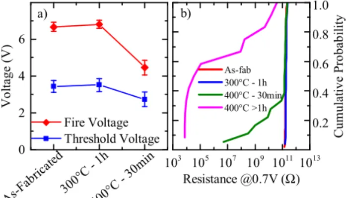
Fig. 1 : Evolution of a) fire (Vfire) and threshold (Vth) voltage and b) OFF-state
resistance after different annealing temperatures. A population of 50 devices is considered for each test reported in this study.
As-F abric ated 300° C - 1 h 400° C - 3 0min 0 2 4 6 b) Fire Voltage Threshold Voltage V olta ge ( V ) a) 103 105 107 109 1011 1013 0.2 0.4 0.6 0.8 1.0 As-fab 300°C - 1h 400°C - 30min 400°C >1h C um ula tiv e Pro ba bility Resistance @0.7V (Ω) 978-1-5386-5247-3/18/$31.00 ©2018 IEEE
reactive sputtering gas. The whole fabrication process temperature never crosses 250°C, allowing the study of the impact of higher temperatures on device performance. In parallel, corresponding OTS thin layers for physico-chemical characterization were deposited at room temperature.
A. DEVICE ELECTRICAL PARAMETERS
As previously reported in the literature, OTS devices need to be initialized by a “fire voltage” (Vfire) before achieving regime
operating parameters [9][10] (i.e. stable Vth). Since fabrication
thermal budget could affect this parameter, we studied its evolution, in addition to that of Vth. All the devices electrical
parameters are acquired by pulse mode characterization, if not differently specified.
The evolution of Vfire and Vth after different annealing steps
is reported in Fig. 1(a). After 1h at 300°C, we observe only a slight increase of Vfire (from 6.7 V to 6.8 V) and Vth (from 3.4 V
to 3.5 V). On the contrary, after 30 minutes at 400°C, both Vfire
and Vth decrease, respectively down to 4.5 V and 2.7 V, with a
reduction of the Vfire/Vth ratio from ~ 2 down to ~ 1.6. The virgin
OFF-state resistance measured at 0.7 V (Fig. 1(b)) is not affected by the annealing at 300°C, whereas the annealing of 30
min at 400°C induces a reduction of the resistance in < 40% of the devices population. A longer annealing at 400°C (> 1h) leads to the loss of the high OFF resistance in almost all the devices.
In order to quantify the leakage current in a "V/2" scheme, we considered the leakage current at Vth/2 (IVth/2). In Fig. 2, we
plot the post-firing subthreshold quasistatic current-vs-voltage (I-V characteristics) mean curves, after the different annealing steps. A leakage current slightly higher than 10 pA is measured before and after the annealing at 300°C. In this case, a change in the conductivity is observed only at voltages higher than 1.7 V (i.e. equal to Vth/2 before the annealing at 400°C). After the
annealing of 30 minutes at 400°C, IVth/2 increases from about
0.01 nA to 0.1 nA, gaining less than one order of magnitude wrt the value before the annealing steps. Despite this increase, the found leakage current is among the lowest reported so far for a backend selector device [11].
B. MATERIAL CHARACTERIZATION
In order to understand the origin of the electrical parameters evolution during the different annealing steps, we performed the physico-chemical analysis on thin N-doped Ge-Se-Sb full sheet amorphous layers. We calculated the optical bandgap (Eg)
evolution after each annealing step, by means of spectroscopic ellipsometry technique performed in the 300-1800 nm spectral region and using a Cody-Lorentz (CL) oscillator (Fig. 3). The
Eg values are extracted from the fitting parameters of the
Fig. 3: Evolution of the optical bandgap (Eg) after different annealing steps at
increasing temperatures. The calculation was performed by fitting the spectroscopic ellipsometry technique results using the Cody-Lorentz model. For each annealing, the heating and cooling rate is 30°C/min and the maximum temperature is maintained during 1 min.
0 100 200 300 1.72 1.76 1.80 1.84 Opt ica l ban dgap Eg (e V ) Temperature (°C)
Fig. 4: XRD measurements performed on full-sheet N-doped Ge-Se-Sb material. No crystalline peak is detected even after an annealing of more than 1h at 400°C. Device failure observed in Fig. 1(b) appears not correlated with a bulk crystallization of the OTS material.
10 20 30 40 50 60 In te ns ity (A .U .) Angle (°) Before Annealing 400°C-30min 400°C >1h
Fig. 2: Evolution of the post-firing I-V characteristics after different annealing steps. A leakage current (IVth/2) slightly higher than 10 pA is measured before
and after the annealing at 300°C. After the annealing of 30 min at 400°C, IVth/2
slightly increases up to ~0.1 nA. The inset shows the full OTS characteristics (pulse mode) for each annealing step.
0 1 2 3 10-12 10-11 10-10 10-9 10-8 10-7 10-6 0 2 4 0 200 400 600
I
Vth/2 Before Anneal.I
Vth/2 After Anneal. Vth/2 Before Anneal. Cu rre nt (A) Voltage (V) Before Annealing 300°C-1h 400°C-30min Post-Firing Subthreshold I-V Characteristics Vth/2 After Anneal. Cu rr en t ( µ A ) Voltage (V) Subthreshold ConductionFig. 5: IR and Raman spectroscopy spectra performed after different annealing steps on Ge-Se-Sb OTS materials. IR spectrum at 300°C highlights the drift of the layer, while the one at 400°C reveals a rearrangement of the structure (i.e. Ge-N bonds).
200 400 600 800
Before Annealing 300°C 400°C-30min
A bs orp tio n (A . U.) Wavenumber (cm-1) Sb-Se Ge-Se Si substrate Ge-N (-)Ge-N(-) 100 200 300 400 Ge-Se ⊗ Sb-Se In te nsi ty ( A . U. ) Raman Shift (cm-1)
ellipsometry measurements using the CL model. Eg increases
up to 300°C and this can be related to a structural relaxation typical of an amorphous chalcogenide material (drift phenomenon) [12]. This relaxation is linked to the defects density reduction, boosted by the increase of the temperature, and it leads to the increase of Vfire after the annealing at 300°C
observed in Fig. 1. Higher temperature Eg measurements were
hindered by the gradual degradation of the encapsulation layer. No crystalline peaks are detected in the X-Ray Diffraction measurements reported in Fig. 4, even after an annealing at 400°C during more than 1 hour. It suggests that the origin of the device failure observed in Fig. 1(b) should not be found in the bulk crystallization of the OTS material, but likely in its interaction with the surrounding co-integrated materials (e.g. electrodes, dielectrics, etc.).
The evolution of the material structure can be further analyzed in the Infrared (IR) and Raman spectroscopy spectra reported in Fig. 5. The slight difference between the spectra of the material as-deposited (before annealing) and after the annealing at 300°C could be representative of the already observed drift phenomenon. It affects all the highlighted bonds, and in particular the ones that correspond to Ge-N (present in a
GeNx phase) and -Ge-N- (bond present as a structural motif
linked to the Ge-Se-Sb phase). Indeed, N atoms are randomly distributed within the Ge-Se-Sb amorphous phase. After the annealing at 400°C we observe a reconfiguration of the Ge-N patterns (only the single Ge-N peak is detected), which is likely the consequence of the creation of a stable GeNx phase in the
layer. The Raman spectroscopy confirms that no homopolar
bonds appear after the annealing at 400°C (which could have led to material partial or total crystallization).
The advantageous reduction of the ratio Vfire/Vth observed in
Fig. 1a after the annealing at 400°C, could be related to a better structural rearrangement of the material. Therefore, we think that the firing operation leads the material to a rearrangement (thanks to the Joule heating), similar to the one observed after the applied annealing at 400°C. It means to us that the structure engineering (e.g. deposition parameters tuning) is as much important as the composition engineering for an OTS device with stable performance since first switching operation (“fire-free device”).
III. ELECTRICAL PARAMETERS EVOLUTION UNDER
TEMPERATURE STRESS
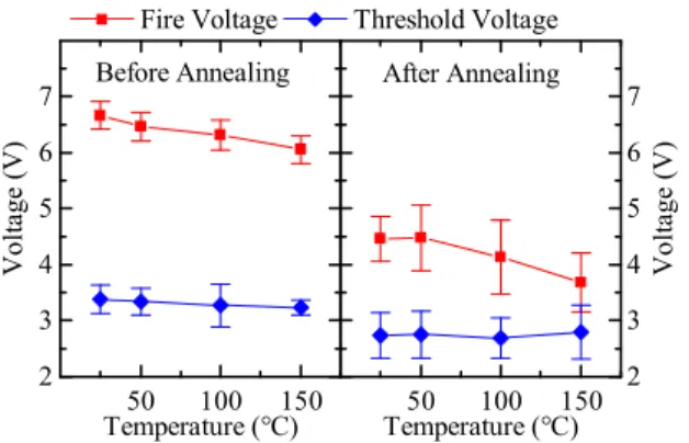
The change of Vfire shows a similar decreasing trend with
increasing stress temperature; moving from room temperature up to a stress temperature of 150°C, before and after the 30 minutes annealing step at 400°C (Fig. 6). The measurement of
Eg (in-situ measurement wrt ex-situ measurement of Fig. 3)
during an equivalent heating of a full-sheet OTS layer up to 150°C exhibits the same linear decrease (Fig. 7). It confirms the strong link between Vfire and the electronic properties of the
material. After the firing, the threshold voltage is almost stable up to 150°C both before and after 400°C annealing.
OTS materials subthreshold electrical conduction can be described by Poole-Frenkel (PF) model [9][13]. The current density J follows equation (1):
Where: σ0 is the zero field conductivity; E is the electric field; Ea
is the energy barrier that can be considered as the energy
exp
(
β E)
T K E exp E σ J b a 0 × × − × × = (1)Fig. 6: Vfire and Vth values for the OTS devices before and after a 30 min
annealing at 400°C, measured under a stress temperature up to 150°C. 50 100 150 2 3 4 5 6 7
Fire Voltage Threshold Voltage
V olt age ( V ) Temperature (°C) Before Annealing 50 100 150 2 3 4 5 6 7 After Annealing V olt age ( V ) Temperature (°C)
Table 1: Parameters of the fitting by Poole-Frenkel model of the I-V characteristics of Fig. 8. σ0 [S/m] Ea [eV] β [√(m/V)] Eg [eV] As-fabricated e6.803 0.824 KbT 5 4 4.632 10 10 195 . 6 × − + × − − 1.762 After 400°C 30min e17.751 1.195 T Kb 4 3 1.017 10 10 993 . 1 × − + × − − 1.659
Fig. 8: Subthreshold conduction measured at different stress temperatures, before and after the 30 min annealing at 400°C on as-fabricated devices. Poole-Frenkel model is used to model the conduction. The fitted parameters are reported in Table 1. 0 1 2 3 4 10-11 10-10 10-9 10-8 After Annealing Exp. Data Model C urr ent (A ) Voltage (V) Before Annealing 0.5 1.0 1.5 2.0 10-11 10-10 10-9 10-8 C urr ent (A ) 25°C 100°C 50°C 150°C Voltage (V)
Fig. 7: Evolution of the optical bandgap (Eg) of as-deposited full sheet material
during in-situ temperature stress. Eg show a linear decrease with the temperature
(as observed in Fig. 6 for Vfire).
50 100 150 1.64 1.68 1.72 1.76 1.80 Opt ica l ban dgap Eg (e V) Temperature (°C)
difference between the conduction band and the localized states; Kb is the Boltzmann’s constant; T is the absolute temperature; β
is the Poole-Frenkel parameter [14]. Fig. 8 reports the quasistatic I-V characteristics performed at different temperatures (from 25°C up to 150°C) on as-fabricated devices before and after the 30 min 400°C annealing, fitted with a PF model (solid lines). The parameters extracted from the fitting are reported in Table 1. The comparison of the calculated activation energy of ~0.82 eV (before annealing) and the optical bandgap of ~1.76 eV (Fig. 3), suggests that the energy of the localized states is located near the middle of the forbidden gap, as previously reported for this class of materials [15]. After the annealing, the activation energy of
the electrical conduction increases from ~0.82 eV up
to ~1.20 eV. We believe that it can be due to the vanishing of the localized states present in the middle of the gap, which could be generated by a high level of disorder suggested by -Ge-N- patterns observed in IR spectrum (Fig. 5), as well disappeared after the annealing.
IV. N-DOPED GE-SE-SB OTSPOST-ANNEALING PERFORMANCE
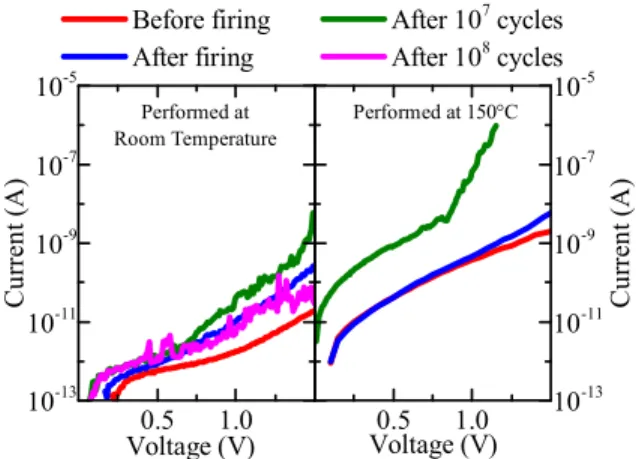
We investigated the endurance performance of N-doped Ge-Se-Sb OTS devices after a 30 min 400°C annealing (Fig. 9) and we acquired the I-V characteristics at the beginning of the test and after 107 cycles (Fig. 10). ON-state current was limited
at ~ 0.2 MA/cm2. Even after 108 cycles, the device exhibits an
ultra-low leakage current (< 0.1 nA @ 1.5 V), close to the post-firing one. This result is ~ 2 orders of magnitude smaller than the previous leakage current reported for an OTS device sustaining such high annealing temperature [16]. The same test was also performed at 150°C. An endurance of more than 107 is
ensured, despites an increase of the leakage current is observed during the cycling.
V. CONCLUSIONS
In this paper, we investigate the stability and the performance at high temperature of N-doped Ge-Se-Sb based Ovonic
Threshold Switching selectors (OTS). Thanks to electrical characterization and material physico-chemical analysis, we show how a BEOL-like thermal budget of 30 minutes at 400°C is beneficial for the reduction of the threshold voltage of the device. We demonstrate that this is achieved by a better structural rearrangement of the material, otherwise achieved only through an initialization firing procedure. After such
thermal budget, an endurance of more than 108 cycles and an
ultra-low leakage current of 0.1 nA, among the lowest reported so far for a backend selector device, are still ensured. Finally, OTS selector operations are demonstrated up to 150°C, showing the suitability of Ge-Se-Sb based OTS selector devices for BEOL integrations, even for applications that target high temperature operating environments.
ACKNOWLEDGMENT
This work has been partially supported by the European 621217 PANACHE Project.
REFERENCES
[1] X. Peng et al., J. Comput. Electron, vol. 16 (4), pp. 1167-1174, 2017 [2] G. Burr et al., J. Vac. Sci. Technol. B, vol. 32 (4), pp. 040802, 2014 [3] S. R. Ovshinsky, Phys. Rev. Lett., vol. 21 (20), 1968.
[4] http://www.techinsights.com/about-techinsights/overview/blog/ intel-3D-xpoint-memory-die-removed-from-intel-optane-pcm/ [5] A. Velea et al., Scientific Reports, vol. 7 (8103), 2017 [6] J. A. Savage et al., Infrared Phys., vol. 5, pp. 195-204, 1965 [7] A. Verdy et al., 2017 IEEE 9th IMW, pp. 1-4, 2017 [8] A. Verdy et al., 2018 IEEE IRPS, accepted, 2018 [9] N.S. Avasarala et al., 2017 47th ESSDERC, pp. 168-171
[10] S.B. Bhanu Prashanth et al., Solid State Commun., vol. 147 (11-12), pp. 452-456, 2008
[11] S.H. Jo et al., 2014 IEEE IEDM, pp. 6.7.1-6.7.4, 2014
[12] P. Noé et al., Semicond. Sci. Technol., vol. (33), pp. 013002, 2018 [13] M.-J. Lee et al., 2012 IEEE IEDM, pp. 2.6.1-2.6.3, 2012
[14] F.-C. Chiu, Adv. Mater. Sci. Eng., vol. 2014 (578168), 2014 [15] J. Luckas et al., J. Mater. Res., vol. 28 (9), pp. 1139-1147, 2013 [16] Y. Koo et al., IEEE Electron Device Lett., vol. 38 (5), pp. 568-571,
2017 Fig. 9: Endurance test performed after a 30 min annealing at 400°C, at room
temperature and under a temperature stress at 150°C. OTS devices are capable of 108 cycles even after annealing (pulse width = 500 ns).
100 102 104 106 108
10-10
10-7
10-4
Performed at Room Temperature OFF-Current @0.2V ON-Current @4.0V Cu rr en t ( A ) 100 102 104 106 108 10-10 10-7 10-4 Performed at 150°C OFF-Current @0.2V ON-Current @4.0V Cycle Tester limit Tester limit
Fig. 10: I-V characteristics performed during the endurance test of Fig. 9. An ultra-low leakage current is ensured even after 107-108 cycles.
Before firing After 107 cycles
After firing After 108 cycles
0.5 1.0 10-13 10-11 10-9 10-7 10-5 Performed at 150°C Cu rr en t ( A ) Voltage (V) Performed at Room Temperature 0.5 1.0 10 -13 10-11 10-9 10-7 10-5 Cu rr en t ( A ) Voltage (V)