HAL Id: cea-01568000
https://hal-cea.archives-ouvertes.fr/cea-01568000
Submitted on 24 Jul 2017
HAL is a multi-disciplinary open access
archive for the deposit and dissemination of
sci-entific research documents, whether they are
pub-lished or not. The documents may come from
teaching and research institutions in France or
abroad, or from public or private research centers.
L’archive ouverte pluridisciplinaire HAL, est
destinée au dépôt et à la diffusion de documents
scientifiques de niveau recherche, publiés ou non,
émanant des établissements d’enseignement et de
recherche français ou étrangers, des laboratoires
publics ou privés.
Silvere Schuermans, Thomas Maurer, Jérôme Martin, Jean-Baptiste Moussy,
Jerome Plain
To cite this version:
Silvere Schuermans, Thomas Maurer, Jérôme Martin, Jean-Baptiste Moussy, Jerome Plain. Plasmon
/ interband transitions coupling in the UV from large scale nanostructured Ni films. Optical Materials
Express, OSA pub, 2017, 7 (6), pp.1787. �10.1364/OME.7.001787�. �cea-01568000�
Plasmon / interband transitions coupling in the
UV from large scale nanostructured Ni films
SILVERE
S
CHUERMANS,1,3THOMAS
MAURER,
1JEROME
MARTIN,
1JEAN-BAPTISTE
MOUSSY,
2 ANDJEROME
PLAIN
1,* 1Université de Technologie de Troyes, Institut Charles Delaunay, Troyes, 10000, France 2Service de Physique de l’Etat Condensé, CEA Saclay, Gif sur Yvette, 91191 cedex, France3silvere.schuermans@utt.fr *jerome.plain@utt.fr
Abstract: We report on the synthesis of Ni nanoparticles via thin film thermal annealing. The as prepared particles exhibit a tunable average diameter ranging from 13 nm to 44 nm depending on the initial deposited film thickness and are covered with a stable NiOxshell. This technique
is suitable for large scale fabrication of Ni nanoparticles onto substrates. The study of the magnetic and optical properties of these nanostructures revealed a ferromagnetic behaviour at room temperature and a localized surface plasmon resonance in the UV-range, promoting Ni nanoparticles as a suitable material for UV-plasmonic applications. The coupling between plasmon and interband transitions have also been studied.
c
2017 Optical Society of America
OCIS codes: (160.4236) Nanomaterials; (160.4760) Optical properties; (310.6188) Spectral properties; (260.3910) Metal optics.
References and links
1. T. Maurer, F. Ott, G. Chaboussant, Y. Soumare, J. Y. Piquemal, and G. Viau, “Magnetic nano wires as permanent magnet materials,” Appl. Phys. Lett. 91(17), 1–5 (2007).
2. S. S. P. Parkin, M. Hayashi, and L. Thomas, “Magnetic domain-wall racetrack memory,” Science 320, 190–194 (2008).
3. Q. A. Pankhurst, J. Connolly, S. K. Jones, and J. Dobson, “Applications of magnetic nanoparticles in biomedicine,” J. Phys. D 36, 167–181 (2003).
4. B. Sepúlveda, J. B. González-Díaz, A. García-Martín, L. M. Lechuga, and G. Armelles, “Plasmon- induced magneto-optical activity in nanosized gold disks,” Phys. Rev. Lett. 104, 1–4 (2010).
5. J. C. Banthí, D. Meneses-Rodríguez, F. García, M. U. González, A. García-Martín, A. Cebollada, and G. Armelles, “High magneto-optical activity and low optical losses in metal-dielectric Au/Co/Au-SiO 2 magnetoplasmonic nanodisks,” Adv. Mat. 24, 36–41 (2012).
6. J. B. González-Díaz, A. García-Martín, J. M. García-Martín, A. Cebollada, G. Armelies, B. Sepúlveda, Y. Alaverdyan, and M. Käll, “Plasmonic Au/Co/Au nanosandwiches with enhanced magneto-optical activity,” Small 4, 202–205 (2008).
7. H. Wang, D. W. Brandl, F. Le, P. Nordlander, and N. J. Halas, “Nanorice: A hybrid plasmonic nanostructure,” Nano Lett. 6, 827–832 (2006).
8. V. Bonanni, S. Bonetti, T. Pakizeh, Z. Pirzadeh, J. Chen, J. Nogués, P. Vavassori, R. Hillenbrand, J. Å kerman, and A. Dmitriev, “Designer magnetoplasmonics with nickel nanoferromagnets,” Nano Lett. 11, 5333–5338 (2011). 9. J. B. González-Díaz, A. García-Martín, G. Amelles, D. Navas, M. Vázquez, K. Nielsch, R. B. Wehrspohn, and U.
Gösele, “Enhanced magneto-optics and size effects in ferromagnetic nanowire arrays,” Adv. Mat. 19, 2643–2647 (2007).
10. J. Chen, P. Albella, Z. Pirzadeh, P. Alonso-González, F. Huth, S. Bonetti, V. Bonanni, J. Å kerman, J. Nogués, P. Vavassori, A. Dmitriev, J. Aizpurua, and R. Hillenbrand, “Plasmonic nickel nanoantennas,” Small 7, 2341–2347 (2011).
11. V. K. Valev, A. V. Silhanek, W. Gillijns, Y. Jeyaram, H. Paddubrouskaya, A. Volodin, C. G. Biris, N. C. Panoiu, B. De Clercq, M. Ameloot, O. A. Aktsipetrov, V. V. Moshchalkov, and T. Verbiest, “Plasmons reveal the direction of magnetization in nickel nanostructures,” ACS Nano 5, 91–96 (2011).
12. T. Pakizeh, “Optical absorption of plasmonic nanoparticles in presence of a local interband transition,” J. Phys. Chem. C 115, 21826–21831 (2011).
13. A. C. Johnston-peck, J. Wang, and J. B. Tracy “Synthesis and Structural and Magnetic characterization of Ni(core)/NiO(shell) nanoparticles,” ACS Nano. 5, 1077–1084 (2009).
14. S. H. Wu and D. H. Chen, “Synthesis and characterization of nickel nanoparticles by hydrazine reduction in ethylene glycol,” J. Coll. Int. Sci. 259, 282–286 (2003).
#281634 https://doi.org/10.1364/OME.7.001787
15. Y. He, X. Li, and M. T. Swihart, “Laser-driven aerosol synthesis of nickel nano- particles,” Chem. Mat. 17, 1017–1026 (2005).
16. K. Nouneh, M. Oyama, R. Diaz, M. Abd-Lefdil, I. V. Kityk, and M. Bousmina, “Nanoscale synthesis and optical features of metallic nickel nanoparticles by wet chemical approaches,” J. All. Comp. 509, 5882–5886 (2011). 17. A. Plaud, A. Sarrazin, J. Béal, J. Proust, P. Royer, J. L. Bijeon, J. Plain, P. M. Adam, and T. Maurer, “Copolymer
template control of gold nanoparticle synthesis via thermal annealing,” J. Nanopart. Res. 15, 1–6 (2013). 18. S. Porel, S. Singh, S. S. Harsha, D. N. Rao, and T. P. Radhakrishnan, “Nanoparticle-embedded polymer : In situ
synthesis, free-standing films with highly monodis- perse silver nanoparticles and optical limiting,” Chem. Mat. 17, 9–12 (2005).
19. J. Martin, J. Proust, D. Gérard, and J. Plain, “Localized surface plasmon resonances in the ultraviolet from large scale nanostructured aluminum films,” Opt. Mater. Express 3, 954–959 (2013).
20. D. Li and S. Komarneni, “Microwave-assisted polyol process for synthesis of Ni nanoparticles,” J. Am. Cer. Soc. 89, 1510–1517 (2006).
21. Z. Pirzadeh, T. Pakizeh, V. Miljkovic, C. Langhammer, and A. Dmitriev, “Plasmon Interband Coupling in Nickel Nanoantennas,” ACS Phot. 1 158–162 (2014).
22. F.J. Garicia de Abajo, http://nanophotonics.csic.es/static/widgets/.
23. P. B. Johnson and R. W. Christy, “Optical constants of the noble metals,” Phys. Rev. B 6 4370–4379 (1972). 24. W. Ni, T. Ambjörnsson, S. P. Apell, H. Chen, and J. Wang, “Observing plasmonic-molecular resonance coupling on
single gold nanorods,” Nano Lett. 10, 77–84 (2010).
25. S. Sako, O. Kazunari, S. Masahiro and B. Shunji, “Magnetic property of NiO ultrafine particles with a small Ni core,” J. Vac. Sci. Tech. B: Microelectronics and Nanometer Structures 15, 1338–1342 (1997).
26. W. J. Moore, "Seven Solid States,” in An Introduction to the Chemistry and Physics of Solids (W. A. Benjamin, 1970).
27. W. H. Meiklejohn and C. P. Bean, “New Magnetic Anisotropy,” Phys. Rev. Lett. 105, 904–913 (1957).
28. T. Maurer, F. Zighem, F. Ott, G. Chaboussant, G. André, Y. Soumare, J. Y. Piquemal, G. Viau, and C. Gatel, “Exchange bias in Co/CoO core-shell nanowires : Role of antiferromagnetic superparamagnetic fluctuations,” Phys. Rev. B 80, 1–9 (2009).
1. Introduction
Many investigations have been reported on Ni, Co or Fe nanoparticles (NPs) due to their ferro-magnetic properties and their high potential for applications in various fields such as permanent magnets [1], racetrack memories [2] or biomedicine [3]. Recently, more attention was paid to nanostructures combining optical and magnetic properties [4–6]. Due to the strong plasmon damping in pure ferromagnetic nanostructures, many studies focused on hybrid nanostructures made of a noble metal layer and a ferromagnetic one. Such hybrid structures have indeed shown enhanced magneto-optical activity [5, 7]. However, few pioneering groups started in-vestigating the possibility to use pure nickel for plasmonics [8, 9]. In particular, it has been evidenced that pure Ni nanostructures exhibit Localized Surface Plasmon Resonances (LSPR) in the UV-visible range [10]. Moreover, Ni nanoparticles offer the possibility to combine LSPR and magneto-optical activity leading to the control of reflected light polarization by both magnetic and plasmonic manipulation [8]. Taking advantage of both magnetic and plasmonic non linear response in G-shaped Ni nanostructures, the possibility to reveal the direction of the magnetiza-tion through the surface plasmon contribumagnetiza-tion to the magnetisamagnetiza-tion-induced second harmonic generation has also been demonstrated [11]. Meanwhile, it has also been shown that a strong coupling between LPSR and interband transitions can occur in Ni nanoantennas [12]. These results open new perspectives for the use of Ni as a magnetoplasmonic material. If electron beam lithography is a suitable nanofabrication process for fundamental studies, other routes more adapted to large-scale Ni NPs synthesis start to be developed like chemical synthesis [13–16]. Among large-scale metallic NPs synthesis routes, thin film thermal annealing has known a great success for gold [17], silver [18], and more recently aluminum [19]. In this study, we propose the adaptation of such process to Ni and evidence the tunability of the NPs LSPR wavelength from 296 nm to 325 nm via a control of the Ni NPs morphology. Structural as well as magnetic and op-tical characterizations have been performed showing, in particular, that the coupling/decoupling between the LSPR and the interband transitions (IBT) might be tuned by an accurate control of the Ni NPs size.
2. Results and discussion
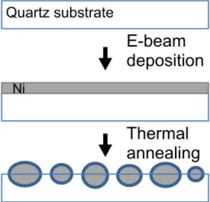
Nanoparticles synthesis. Silicon or glass substrates were cleaned in successive ultra-sonic baths of (1) surfactant (Decon 90) mixed with water (2) isopropanol, (3) acetone and (4) pure isopropanol for rinsing before being dried under Ar flux. In the next step, a Ni thin film was deposited under vacuum (7.5 10−8Torr) using e-beam evaporator. The layer thickness was set from 5nm to 15nm depending on the targeted Ni particles diameter. Then thermal annealing was proceeded under vacuum (8 10−5 Torr) using a Rapid Thermal Annealing (RTA) oven. The samples were annealed at 800◦Celsius degrees during 5 min. This process, schematically summarized in Fig. 1, is based on the Ni film dewetting and leads to the formation of quasi-hemispherical Ni NPs.
E-beam
deposition
Thermal
annealing
Quartz substrate NiFig. 1. Scheme of the synthesis process. A thin Ni layer is deposited by e-beam evaporator in vacuum then this layer is annealed at low pressure.
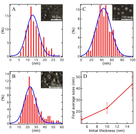
For initial layer thicknesses of 5, 10 and 15nm, we measured a final average diameter of respectively 13 ± 8.9nm, 23 ± 15.6nm and 44 ± 34.1 nm respectively. Particles size distributions are presented in Figs. 2(a), 2(b) and 2(c). A clear correlation is noticeable between the final average particles size and the initial thickness of Ni layer as shown in Fig. 2(d). Conversely, for a deposited Ni film thickness larger than 20 nm, the dewetting is not complete and a percolated film is observed.
Optical characterization. Optical properties of the Ni NPs have been analyzed using extinc-tion measurements performed in a UV-Visible spectrophotometer. Incident light comes from a deuterium arc lamp. The extinction spectra of the Ni NPs have been measured with a transmission optical microscope coupled to a micro-spectrometer using a multimode optical fiber as confocal filtering. A 100 × objective lens (N A= 0, 96) allows for a detection area of about 100µm2.
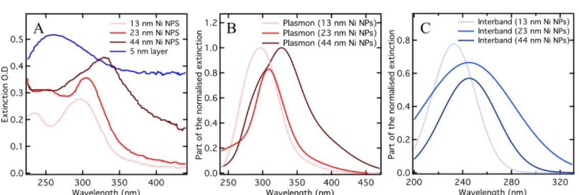
Figure 3(a) shows a comparison between the extinction spectra of a typical thin film and of Ni NPs obtained after thermal annealing of the thin film. Optical extinction spectra for the 5nm thin film exhibit only one peak around 250 nm while those for Ni NPs obtained after thermal annealing of the thin film show two peaks.
Deconvolutions of the experimental optical spectra were undertaken in order to put into evidence the size dependency of these two peaks in Figs. 3(b) and 3(c). The first low-wavelength peak is around 250 nm and slightly red-shifted for bigger Ni NPs. The second one is located in the spectral range 290 nm - 330 nm and is strongly red-shifted for larger Ni NPs. Thus the large-wavelength peak exhibits a strong spectral size-dependency- characteristic of Localized Surface Plasmons- and the related wavelengths are in agreement with the literature [20]. This confirms the formation of Ni NPs during the annealing process. The low-wavelength peak,
D
A
B
C
50 nm 200 nm 100 nm
Fig. 2. A, B and C: Size distribution of Ni particles after dewetting of a Ni layer whose initial thickness is 5 nm (A), 10 nm (B) and 15 nm (C). SEM pictures correspond to each size distribution with a scale bar of 200 nm. The average diameter is assessed to 13, 23 and 44 nm respectively. The Full-Width at High Maximum (FWHM) is 8.9 nm, 15.6 nm and 34.1 nm for graph A, B, C, respectively, which indicates a relative dispersion of Ni size. D: evolution of the average size of Ni particles depending on the initial layer thickness. The balance bar corresponds to the FWHM for each average size.The NPs sizes were determined by statistical SEM images analysis over more than 300 NPs.
located around 250 nm for all the samples, is typical of the interband transitions (IBT) [21] and its spectral dependency will be discussed later in the article.
We first tried to retrieve our experimental data by Mie theory calculation performed by freely available code [22] with an external refracting index of 1.26 which corresponds to the average of the real part of the refracting index around our NPs. However, the numerical optical extinction spectra exhibit LSPR which are much more blue-shifted compared to the experimental ones. Therefore the discrepancy between experimental and the Mie theory has enabled us to come up with the hypothesis that the Ni NPs are partially oxidized and covered with a NiOxshell. The
oxidation probably takes place during the annealing process because of residual oxygen in the oven and forms a passivation layer [13] which probably explains the chemical stability of the NPs and their optical properties in time. Consequently, we tried to introduce a dielectric NiOxshell
C
A B
Fig. 3. A: Extinction spectrum of Ni layer of 5 nm thick, before thermal annealing (blue curve) and after thermal annealing (pink curve). The interband transitions peak and the plasmonic peak are visible on the pink curve respectively at 233 nm and 296 nm. The 10 nm layer after annealing is represented by the red curve and the 15 nm layer after annealing by the brown curve. B: Spectrum of the plasmonic component from the extinction spectrum of Ni particles obtained by thermal annealing of 5 nm thick (pink curve), 10 nm thick (red curve) and 15 nm thick (brown curve). C: Spectrum of the interband transitions component from the extinction spectrum of Ni particles obtained by thermal annealing of 5 nm thick (light blue curve), 10 nm thick (blue curve) and 15 nm thick (dark blue curve).
with variable thickness in our Mie calculations. We varied the NiOxshell thickness from 0 nm to
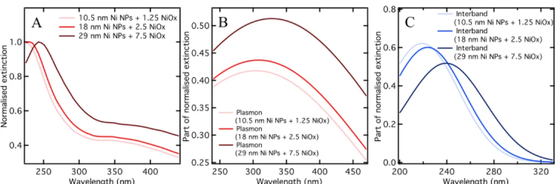
a maximum thickness corresponding of the NP radius. In order to compare experimental and numerical data, we proceeded to a deconvolution of the overlapping IBT and LSPR peaks. Using the procedure described above we present in Fig. 4(a) the calculated spectra for Ni nanoparticles of 13 nm, 23 nm and 44 nm diameter with a shell thicknesses of 1.25 nm, 2.5 nm and 7.5 nm respectively. The LSPR peaks are deduced from those spectra in Fig. 4(b). It appears that LSPR peaks are located at 296, 308 and 327 nm.
Similarly, in Fig. 4(c) the IBT peak wavelength using the Mie theory is 218, 224 and 240 nm for thickness of 13 nm, 23 nm and 44 nm. The calculated LSPR wavelengths are in full agreement with the experimental results. The calculated IBT wavelength presented in Fig. 4(c) wavelength shows a slight discrepancy of about 13.7 nm in average. Therefore, the comparison between calculated and experimental optical extinction spectra tends to confirm the presence of a NiOxshell around the Ni NPs.
Further SEM measurements on the largest particles were taken to confirm the presence of a NiOx shell. Due to the backscattered electron’s energy (which is sensitive to the electronic
density of the material) we could visualize the shell position on the surface of the largest NPs. We measured the contrast difference on the SEM images shown in Fig. 5(a) to retrieve the shell thickness. The thicknesses distribution in Fig. 5(b) was fitted by a gaussian curve yielding to an average thickness of 7.8 nm. This value is close to the calculated one of 7.5 nm. Those experimental measurements are thus in good agreement with the prediction of a NiOxshell and
with the Mie calculation.
Besides, in order to better understand the size dependency of the LSPR and IBT wavelengths, we proceeded to mathematical deconvolutions of the experimental optical extinction spectra. Such deconvolutions were done using multiple gaussian peak fitting. The results are shown in Fig. 3(b) for the LSPR and in Fig. 3(c) for the IBTs, respectively. They indicate as expected that the LSPR wavelengths are respectively 296, 308 and 327 nm for 13, 23 and 44 nm large in average Ni NPs. The LSPR shift with the Ni NPs size is due to the increased polarizability of the NPs. In Fig. 3(a) it can also be observed that the absorbance increases with increasing
C
A B
Fig. 4. A: Calculated extinction spectrum of Ni nanoparticles of 10.5, 18, and 29 nm diameter with an external refracting index of 1.32. The corresponding shell thickness are 1.25, 2.5 and 7.5 nm. B: Plasmonic component from the theoretical extinction spectrum of Ni particles obtained by thermal annealing. C: Spectrum of the interband transitions component from the theoretical extinction spectrum of Ni particles
Shell thikness distribution
A B
Fig. 5. A: SEM image of Ni NPs whose diameter distribution is centered at 44nm. The shell is visible by the difference of contrast on the surface of the NPs. The scale bar is 100 nm. B: Thickness distribution of measured shell thickness on SEM images. The average value of 7.8 nm is determined by Gaussian fit on measurement.
particle size, which is due to the increase of the extinction cross section. As for the Ni NPs IBT wavelength presented in Fig. 3(c), it exhibits a slight redshift of about 12nm for all the NP diameters as well as a strong decrease of the intensity. This shift was not apriori expected because the interband transitions only depend on the bulk physical properties [23]. However this kind of observation has recently been discussed [12] and experimentally evidenced [21], thus confirming our experimental results. The IBT shift which is here observed is in fact characteristic of strongly coupled system [24]. In our case, it deals with strong coupling between LSPR and interband transitions [21]. When the Ni NPs size increases, a splitting is noticeable by the IBT red shift. In concordance with this splitting, the optical density of the IBT is significantly reduced while the NPs grow larger and larger. Indeed, for the average particle diameter of 13 nm, 23 nm and 44 nm, the optical density of the interband transitions are respectively of 0.077, 0.066 and 0.057. So by changing the particles sizes, it is possible to tune and decrease the contribution from the interband transitions to the optical extinction of the system.
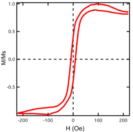
Magnetic characterization. The magnetic properties at room temperature of such NiOx@Ni
NPs were characterized using a vibrating sample magnetometer (VSM) with the external field applied in the plane of the sample. Figure 6 presents the hysteresis cycle of Ni particles obtained by thermal annealing of a 10 nm thick Ni layer (for NPs with an average size of 23 ± 4.7 nm). It shows that the as-prepared Ni NPs are ferromagnetic at room temperature exhibiting a coercitivity of 95 Oe. Bulk NiOxis known to be anti-ferromagnetic [25] with a Neel temperature
TN=523K [26]. The presence of an antiferromagnetic shell around the Ni NPs should thus induce
exchange bias [27] at room temperature. However, the experimental hysteresis cycle is symmetric and no exchange bias is observed with our samples at room temperature. One explanation for the absence of exchange bias at room temperature might come from a superparamagnetic behaviour of the NiOxshell at room temperature [28] due its nanometric size.
H (Oe)
M/Ms
Fig. 6. Hysteresis cycle of the Ni particles obtained by thermal annealing of a 10nm Ni thin film layer. The hysteresis cycle was measured at room temperature using a vibrating sample magnetometer (VSM).
3. Conclusion
To conclude it has been here demonstrated that the dewetting of thin films may lead to the formation of NiOx@Ni nanoparticles with well-controlled sizes in the range of 13-44 nm. The
as-prepared NiOx@Ni NPs exhibit interesting plasmonic properties in the UV spectral range, in
particular a Localized Surface Plasmon Resonance around 300nm which may couple with the interband transitions peak fo the smallest Ni NPs. Moreover, it has been shown that although the NiOxlayer does not generate exchange bias due to its too thin thickness, it contributes to the
spectral redshift of the LSPR peak above 250nm when compared Ni NPs without any oxide layer. That could be highly interesting to look for coupling effect between fluorophores emmitting in the UV range and Ni particles without absorption from the interband transition. Another promising application for these magnetoplasmonic NPs could lie in UV circular dichroism. Funding
The authors thank the French Nationale Reaserarch Agency (ANR NATO, Grand ANR-13-BS10-0013-03) and the Labex ACTION project (contract ANR-11-LABX-01-01). Financial support of NanoMat (www.nanomat.eu) by the"Ministère de l’enseignement supérieur et de la recherche," the "Conseil régional Champagne-Ardenne," the "Fonds Européen de Développement Régional (FEDER)," and the "Conseil général de l’Aube".