Characterization and Modeling of
Plasma Etch Pattern Dependencies
in Integrated Circuits
By
Kwaku O. Abrokwah
Submitted to the Department of Electrical Engineering and Computer Science in Partial Fulfillment of the Requirements for the Degree of
Master of Engineering in Electrical Engineering and Computer Scienc MASSACHUSS INSTTEMASSACHUSETTS INSTrl JE •
OF TECHNOLOGY at the Massachusetts Institute of Technology
AUG
1 4 2006
February 6, 2006LIBRARIES
© Massachusetts Institute of Technology, 2006. All Rights Reserved. LIBRARIES
Author -. - I , ,
Electrical Engineering and Computer Science February 6, 2006
Certified by- - -
-,v~-Duan 4 . Boning Professor of Electrical Engineering and Computer Science Thesis Supervisor
Accepted by
Arthur C. Smith Chairman, Department Committee on Graduate Studies Electrical Engineering and Computer Science
Characterization and Modeling of
of Plasma Etch Pattern Dependencies
in Integrated Circuits
By
Kwaku O. Abrokwah
Submitted to the
Department of Electrical Engineering and Computer Science February 6, 2006
In Partial Fulfillment of the Requirements for the Degree of Master of Engineering in Electrical Engineering and Computer Science
ABSTRACT
A quantitative model capturing pattern dependent effects in plasma etching of
integrated circuits (ICs) is presented. Plasma etching is a key process for pattern formation in IC manufacturing. Unfortunately, pattern dependent non-uniformities arise in plasma etching due to microloading and RIE lag. This thesis contributes a semi-empirical methodology for capturing and modeling microloading, RIE lag, and related pattern dependent effects. We apply this methodology to the study of interconnect trench etching, and show that an integrated model is able to predict both pattern density and feature size dependent non-uniformities in trench depth.
Previous studies of variation in plasma etching have characterized microloading (due to pattern density), and RIE lag (aspect ratio dependent etching or ARDE) as distinct causes of etch non-uniformity for individual features. In contrast to these previous works, we present here a characterization and computational methodology for predicting IC etch variation on a chip scale that integrates both layout pattern density and feature scale or ARDE dependencies. The proposed integrated model performs well in predicting etch variation as compared to a pattern density only or feature scale only model.
Thesis Supervisor: Duane S. Boning
Acknowledgements
I would like to first thank my advisor, Duane S. Boning, for the opportunity to work
in his group. Without his guidance, I would not have reached this milestone. I would like to continue by thanking the current and past members of the Statistical Metrology Group who have been there for me by giving me the inspirations that have allowed me to progress. Tyrone Frank Hill, Karen Mercedes Gonzailez-Valentin Gettings, Mehdi Gazor, Brian Tang, Tae Hong Park, Hayden Taylor, Xiaolin Xie, Hong Cai, Shawn Staker, Nigel Drego, Karthik Balakrishnan, and Daihyun Lim, thank you for your friendship.
I would like to thank my family for the love, guidance, and support they have
provided me with throughout my life. I certainly could not have made it this far without them.
I would also like to especially thank my friend Oluwamuyiwa Oluwabudye, who has
guided and tutored me throughout my MIT career. Thank you for your encouragement and thoughtful insights about college, graduate school, and life in general.
This work could not have taken place without the support of Texas Instruments and Praesagus, Inc. I would like to thank Tamba Tugbawa for his help with the metrology part of this thesis research and Aaron Gower for the various discussions we had about the etch non-uniformity. I would like to thank PR Chidambaram for his supervisory role in making the experiment at TI possible. Lastly, I would like to thank the Semiconductor Research Corporation for awarding me a masters fellowship that has allowed me to pursue this thesis work.
Table of Contents
B y ... ... ... ... 3
ABSTRACT ... .. ... 3
Acknow ledgem ents ... ... 4
Chapter 1 Introduction and M otivation for Research ... 9
1.1 M otivation and O verview ... ... 9
1.2 O verview of Plasm a Etching ... 10
1.2.1 Physical and Chemical Process in Plasma Etching... 11
1.3 Previous W ork ... ... 12
1.4 Sum m ary... 13
Chapter 2 Theory of the Causes of Plasm a Etching N on-uniform ity ... 14
2.1 V ocabulary ... ... 14
2.2 Sources of N on-uniform ity ... 16
2.3 Cham ber Induced N on-uniform ity... 19
2.3.1 Plasm a G eneration... ... 20
2.3.2 Etch Species, Tem perature, and By-products ... 22
2.3.3 Ion Flux D istribution ... 24
2.3.4 N eutral Flux D istribution... 24
2.3.5 Ion N eutral Synergism ... 26
2.4 Pattern Induced N on-uniform ity ... 28
2.4.1 W afer Level N on-uniform ity ... 29
2.4.2 D ie Level N on-uniform ity ... 30
2.4.3 Feature Level N on-uniform ity ... 32
2.5 Aspect Ratio D ependent ... 32
2.5.1 Ion Shadowing ... 33
2.5.2 N eutral Shadowing ... 34
2.5.3 K nudsen Transport ... ... 35
2.6 Sum m ary... ... 36
Chapter 3 M ask D escription ... 37
3.1 M ask Floor Plan... ... 37
3.2 Capacitance/Com b Structures... 40
3.3 Line W idth Line Space Structures ... 41
3.4 Sum m ary ... 44
Chapter 4 Experim ent in N on-uniform ity of D ielectric Plasm a Etch ... 45
4.1 M otivation ... ... 46
4.2 Critical Dimension Process Flow ... 47
4.3 D epth Process Flow ... 49
4.4 OPC and Lithography ... 51
4.5 Progression of V ariations... 53
4.6 Sum m ary... 54
Chapter 5 M etrology and Characterization ... 55
5.1 Critical D im ension Scanning Electron M icroscopy... 55
5.1.1 CD SEM M easurem ent Plan... 56
5.1.2 CD SEM M easurem ent Results ... 58
5.2 Profile Scanning Electron M icroscope ... ... ... 61
5.2.1 M easurem ent Plan ... ... 62
5.2.2 M easurem ent Results... 63
5.3 D epth Trends ... ... 66
5.3.1 D epth Trends ... 67
5.3.2 Analysis of V ariance... 70
5.4 Sum m ary... ... 73
Chapter 6 A Pattern D ensity Based Etch Prediction M odel ... ... 74
6.1 D escription of M odel ... ... 74
6.2.1 Physical M otivation for Pattern D ensity Effect ... ... 76
6.2.2 Effective Pattern D ensity ... 78
6.2.3 Filter D escription ... 78
6.2.4 Pattern D ensity M odel Im plem entation ... ... ... 82
6.3 M odel Prediction ... 83
6.3.1 Filter Com parison ... 84
6.3.2 M odel Results ... 87
6.4 Lim itations of M odel ... 90
6.5 Sum m ary... ... 90
Chapter 7 A Feature Based Etch Prediction M odel... ... 92
7.1 Coburn and W inters M odel... 93
7.1.1 M odel D escription ... 93
7.2 M odel Results ... 95
7.3 Sum m ary... ... 96
Chapter 8 A n Integrated Etch Prediction M odel... 97
8.1 M odel D escription ... 97
8.2 M odel Results ... 98
8.3 Sum m ary ... ... ... ... 101
Chapter 9 Conclusion and Future W ork ... 102
9.1 Pattern D ensity M odel Conclusion and Future W ork... ... 102
9.2 Feature Based M odel Conclusion and Future W ork... ... 103
9.3 Integrated M odel Conclusion and Future W ork ... ... 104
9.4 W afer Level M odel ... ... 104
9.5 Sum m ary... ... ... 104
References ... ... 106
Table of Figures
Figure 1-1 - Schematic of inductively coupled plasma etching chamber [2]... 11
Figure 2-1 - Profile of plasma etching non-uniformity causes and effects [7]... ... 17
Figure 2-2 - Sources of non-uniformity in plasma etch ... ... 19
Figure 2-3 - Asymmetric gas flow and chamber design [9] ... ... 21
Figure 2-4 - (a) Effect of pressure on etch rate [4] and (b) effect of chemistry on etch rate [4] ... 23
Figure 2-5 - (a) Schematic of ideal ion flux versus (b) real ion flux with distribution of energies (velocities) an d an g le s ... ... 2 4 Figure 2-6 - (a) Schematic of ideal neutral flux versus (b) real neutral flux... ... 25
Figure 2-7 - (a) Ion flux map and (b) neutral flux map for DRIE etch process [11]... 28
Figure 2-8 - (a) Global etch map for 0.06% loading, which features a hot spot at the middle left part of the wafer [12]. (b) Global etch map for 17.6% loading, featuring a cold spot at the upper right region of th e w afer [12 ] ... 3 0 Figure 2-9 - Schematic of the depletion of reactants due to microloading... 31
Figure 2-10 -Schematic of feature non-uniformity. Structures with different critical dimension (CD) etch at different rates due to ARDE effects... 32
Figure 2-11 -Illustration of shadowing effect [16]... 34
Figure 2-12 -Schematic of Knudsen transport between two chambers ... ... 35
Figure 2-13 -Plot of Knudsen transmission probability, K ... 36
Figure 3-1 - Schematic of copper mask along with line widths and line spaces for each capacitance and line w idth and space structure (in pm ) ... 38
Figure 3-2 - The design space of line widths and spaces encompassed by the capacitance and line width and space structures ... ... 39
Figure 3-3 - T est m ask layout ... ... 40
Figure 3-4 - Capacitance structures ... 41
Figure 3-5 - Line width and space structures ... 42
Figure 3-6 - Close up view of a line width and space module with line width and line space of 10 jim and density of 50 % ... ... ... ... ... 4 3 Figure 4-1 - CD process post-etch stack profile... ... 49
Figure 4-2 - Depth process post-etch stack profile ... ... 50
Figure 4-3 - D esigned structure L 24 ... 52
Figure 4-4 - OPC correction on L24 ... ... 52
Figure 4-5 - Variations introduced in the OPC, lithography, and etch processes ... 53
Figure 5-1 - (a) Structures of interest on the test mask. (b) Map of line width and line space of all stru c tu re s... 5 7 Figure 5-2 - (a) Four dies measured per wafer and (b) nine quadrants measured per structure...58
Figure 5-3 - (a) Post lithographic and (b) post etch SEM of capacitance structure, CA3...59
Figure 5-4 - Setup of VeritySEM tool for profile measurements ... 61
Figure 5-5 - Measurement process of VeritySEM tool ... 62
Figure 5-6 - Measurement plan for profile and depth measurements of structures... 63
Figure 5-7 - Location of (a) dies and (b) measurement points measured for each wafer and structure, respectively ... 63
Figure 5-8 - Profile measurement results for (a) 0.1 tm and (b) 6 im capacitance structures showing line and edge roughness ... 64
Figure 5-9 - Profile measurement results for 0.1 jim capacitance structure showing faceting and slopped sidewall ... 65
Figure 5-10 -Profile measurement results for 6 Im capacitance structure showing faceting and slopped sid w a ll ... 6 6 Figure 5-11 -Measured depth for fixed line width of 0.1 Im ... 67
Figure 5-12 - Measured depth for a fixed line width of I jim... ... 68
Figure 5-13 - Measured depth for a fixed line space of 1 im ... ... 69
Figure 5-14 - Measured depth for a fixed pitch between I and 1.2 jim ... ... 70
Figure 5-16 - Mean and one standard deviation depth grouped by die ... 72
Figure 6-1 - Overall plasma etch model architecture ... 76
Figure 6-2 - Reactant concentration as a function of distance from etching feature...79
Figure 6-3 - (a) Inverse, (b) Gaussian, and (c) Elliptical filter shapes [21] ... 81
Figure 6-4 - Local layout pattern density, extracted from a mask layout on a discretized grid across the chip, is convolved with an etch impulse response or averaging filter. The result is the effective pattern density across the chip. The vertical axis of the effective pattern density is in percentage... 82
Figure 6-5 - Spatial location on test die of depth measurements; the coordinates indicate the spatial location of structures and measurement points on the chip (in 20x pm). (a) Local layout pattern density with (b) locations of measurements. (c) Location of 100 nm (0.1 /m) line width structures. (d) Location of structures with line widths greater than 3000 nm (3 tm) ... 84
Figure 6-6 - (Top row) Effective pattern density using gaussian filter with filter width of 20 mti, (middle row) filter width of 600 Im, (bottom row) filter width of 2000 tm ... 86
Figure 6-7 - (Top row) Effective pattern density using inverse distance filter with filter width of 20 tim, (middle row) filter width of 600 /m, (bottom row) filter width of 2000 jm ... 87
Figure 6-8 - 3D view of effective pattern density, as extracted using the pattern density only model... 88
Figure 6-9 - Chip-scale simulation of etch depth (in nm) using the pattern density only model ... 89
Figure 6-10 - Simulated and experimental etch depth. Simulations are based on the pattern density only model for 0.1 #m features. The rms error is 4.5% ... 89
Figure 7-1 - Schematic of etchant flux in narrow trench feature... 94
Figure 7-2 - Feature based model comparison to measurement data. Overall fit has 7.3% rms error... 95
Figure 7-3 - Chip-scale simulation using the feature based only model. The scale indicates the predicted etch depth (in nm)... ... ... 96
Figure 8-1 - 3D view of effective pattern density for integrated etch model ... 99
Figure 8-2 - Chip-scale simulation of etch depth using the integrated model. The scale indicates the predicted depth (in nm) based on both pattern density and aspect ratio ... 100
Figure 8-3 - Comparison of integrated model prediction and measurement data (top); as function of line width (middle); as function of pattern density (bottom)... ... 100
Chapter I
Introduction and Motivation for Research
This thesis presents the motivation for studying variation in plasma etching of integrated circuit (IC) interlayer dielectrics (ILD) due to pattern dependencies. We also motivate the need for accurate prediction and modeling. After describing the physical processes involved in plasma etch, previous work in the field is presented. This thesis attempts to capture IC dielectric etch variation through an integrated pattern density and aspect ratio based model that can simulate within and across die variation in etch depth for all feature sizes.
1.1 Motivation and Overview
As integrated circuits follow a path of shrinking technology scale, the percentage of performance variation due to back end of the line processes has increased to the point whereby it is comparable to that of transistor variations [1]. Plasma etching of interlayer dielectrics (ILD) for metal contacts, vias, and lines is a significant contributor to chip-scale circuit performance variations. These performance variations manifest themselves in terms of varying resistance and capacitance across the chip and lead to circuit signal delays and skews [1].
This thesis has three goals. The first is to develop a computationally efficient chip scale pattern density model based on the physical process of plasma etching. The second is to develop a chip scale feature-level or aspect ratio dependent etch (ARDE) model based on plasma etchant transport dynamics. Lastly, this thesis will integrate the pattern density and feature level models into a combined model, and show how the combined model provides superior prediction to the individual models.
Chapter 2 will describe in detail the theories behind the causes of plasma etch variations at the wafer, die, and feature levels. Chapter 3 describes the mask layout of the test chip used to obtain empirical data for our model development and for characterizing variations seen in plasma etch of ICs. Next, Chapter 4 describes the etch experiment conducted using the test mask. Chapter 5 presents the metrology taken on the test wafers and Chapter 6 and Chapter 7 develop the two etch models: a pattern density model and a feature based (aspect ratio dependent etch) model. Chapter 8 presents the integrated model that combines the pattern density and feature based models, and demonstrates the ability of the integrated model to effectively predict chip scale etch variations. Lastly, Chapter 9 concludes the thesis.
1.2 Overview of Plasma Etching
Plasma etching is a key process for pattern formation in IC manufacturing. Plasma etching allows for anisotropic and selective etching of material layers in both front end and back end IC process steps. In the front end processes of transistor formation, plasma etching is used to etch shallow trench isolation (STI) structures, and form the polysilicon gate. In the back end processes, plasma etching is used for contacts, vias, and trench line formation.
Figure 1.1 illustrates a schematic of an inductively coupled plasma etcher. The etching process occurs in a vacuum chamber regulated by an automatic pressure controller (APC). The top of the chamber has an inlet and showerhead where the feed gas such as carbon tetraflouride (CF4) enters and is ignited into the etching plasma. This ignition is induced and maintained by the radio frequency (RF) coils that wrap around the chamber and typically operate at 2 MHz with RF power between 0 and 1000 watts. The
substrate holder or chuck is RF biased at 13.56 MHz with power between 0 and 1000 watts. The chuck also has a helium cooling gas inlet that cools the backside of the wafer
and regulates the wafer temperature.
Figure 1-1 - Schematic of inductively coupled plasma etching chamber [2]. 1.2.1 Physical and Chemical Process in Plasma Etching
Plasma etching involves the ionization of chemical gas into ion and neutral plasma. For oxide (SiO2) etching, the initial gas is usually a carbon fluorine molecule such as carbon tetraflouride (CF4). The ionized plasma within the chamber is accelerated towards the wafer holding chuck through the RF bias on the chuck which creates a strong electric field with the plasma. The space between the plasma and the wafer is called the sheath. The ions pick up most of their energy when they enter the sheath and are accelerated by the electric field. The neutral plasma diffuses from the plasma through the sheath and towards the wafer. The method of diffusion is highly debated within the semiconductor industry and academia [3].
Although some isotropic diffusion of the neutrals takes place, there is evidence that collisions between neutrals, ions, and electrons create fast neutrals that do not behave isotropically [4]. These fast neutrals, along with other causes of non-uniform distributions of neutrals within the etch chamber, are discussed in Chapter 2. The interaction of ions and neutrals once they reach the wafer surface is discussed in Chapter 6 and Chapter 7. 1.3 Previous Work
Previous works in modeling non-uniformities in plasma etch have generally focused on three areas that correspond to three length scales. The first area where non-uniform etch rate was encountered is across wafer or wafer-to-wafer etch variation. This variation, termed macroloading, is the longest length scale where non-uniform etching occurs. Industry engineers and academic scientists first noticed macroloading when the etch rate of one wafer varied from the etch rate of another wafer due to the amount of exposed area being etched [5]. Macroloading was also noticed within the wafer whereby different regions of the wafer, having differing amounts of open area, etch at different rates [5].
The next area of non-uniformity corresponds to the length scale of within die and between die. This length scale of variation is termed microloading because it corresponds to localized variation in reactant depletion that cause etch rate non-uniformity. Areas within the die with more exposed surface area etch more slowly than areas with less exposed surface area. Microloading differs from macroloading both in their length scales and their effect on the etch rate. While macroloading increase the reactant loss rate throughout the reactor and loads down the reactant concentration, near the reactive surfaces, the reactant concentration is depleted further due to microloading [4].
Microloading causes and effects are described in Chapter 2 and form the basis of our modeling work in this thesis, along with aspect ratio dependent etching.
The third area of non-uniformity corresponds to the length scale of individual features. Variations at this length scale are termed aspect ratio dependent etching. The mechanisms of ARDE act independently of macroloading and microloading. Industry engineers and academic researchers have focused on transport of ions and neutrals within a microstructure as the mechanism by which ARDE occurs [4][6]. The cause and effects of ARDE are discussed in Chapter 2.
1.4 Summary
Layout induced etch variation within integrated circuit manufacturing becomes more pronounced as the industry technology evolves. This thesis is devoted to first understanding the sources of etch rate non-uniformity, and then presenting a methodology for effectively capturing etch rate variation at the chip scale based on layout pattern dependencies. The following chapters present the theories underpinning our methodology and the development of pattern density and feature level models from the methodology.
Chapter 2
Theory of the Causes of Plasma Etching Non-uniformity
In this chapter the spatial and physical sources of plasma etch non-uniformity are described, along with models that explain the interactions between the physical processes and the spatial variations. The physical processes include the chemistry of the plasma and the characteristics of the chamber generating the plasma. Much of the chemistry involved in plasma etching was described in Chapter 1. The spatial variations depend on the size and arrangement of features on the wafer and the evolution of these features throughout the etch process. The trench evolution is dictated by the interactions of the plasma species
with the substrate being etched.
Although this section will review most of the causes and effects of plasma etch non-uniformity, this thesis primarily focuses on microloading and ARDE which are caused by transport of chemical etch species. In Section 2.1 the common terminology used to describe pattern dependent effects in RIE are defined and categorized. Next, Section 2.2 discusses the sources of variations seen in the etch rates and profiles of structures. Section 2.3 expands on one of two sources of variations, chamber induced uniformity. Section 2.4 describes the second source of variation, pattern induced non-uniformity. Section 2.5 focuses on the most commonly encountered RIE effects. Finally the conclusion in Section 2.6 revisits all the causes and effects of variations seen in plasma etch.
2.1 Vocabulary
Non-uniformities in plasma etch processes have been studied continuously over the past 30 years. As a result, terminology has emerged for describing these variations.
Specifically, microloading, reactive ion etch lag (RIE-lag), aspect ratio dependent etching (ARDE), ion shadowing, and neutral shadowing merit discussion. These term arose to describe the causes and effects of etch rate non-uniformity. Often many terms overlap such as RIE-lag and ARDE.
Microloading describes competition for and depletion of reactive etching agents when exposed to loading across a chip, and results from similar mechanisms to those that cause macroloading [4]. Microloading should only be used to refer to a local dependence on pattern density for identical features. Section 2.4 further describes the causes and effects of microloading.
RIE-lag and ARDE describe non-uniformity arising from the aspect ratio of individual features. Aspect ratio is defined as the ratio between the depth of a microstructure and its width. Ion and neutral shadowing are one of many means by which RIE lag and ARDE occurs. Gottscho describes RIE lag as resulting from microscopic transport phenomena within a single feature. It is possible to have RIE-lag without microloading and vice versa [4]. In the subsequent sections of this chapter, we describe both the physical, descriptive, and analytical models that have been used to study RIE-lag.
Although used interchangeably, RIE-lag is a manifestation of ARDE, which is synonymous with aperture or proximity effect [4]. The term was coined by researchers at IBM to describe the common observation that smaller diameter trenches and holes etch more slowly than larger diameter trenches and holes [4]. This effect is also evident in the etching of post structures, where the etch rate near the post can be less than the etch rate in the open area between the posts [4]. RIE lag refers to the dependence of etch rate on aspect ratio (depth/width). Unlike microloading, RIE-lag is characteristic of individual
microstructures. It does not depend on absolute feature size but only on aspect ratio. Therefore, because aspect ratio continually increases during the etching process, etch rates are necessarily time dependent [4].
Etch rate and profile deviations depend on the interactions of microstructures and etchant species [4]. Ion and neutral transport encompass the majority of the causes of etch rate and profile variations [4][7]. The cause and effect of microloading and ARDE are shown in Table 2-1. The three causes of RIE-lag are transport of reactive species, ion shadowing and neutral shadowing (Table 2-1). In most cases of RIE-lag, there is a decrease in etch rate with increasing aspect ratio. This is often called "positive" or "ordinary" RIE lag and is mostly caused by diminishing probability of reactants reaching
the bottom of the etching structure [6]. But when RIE-lag is caused by shadowing of reactants, there can be acceleration in reaction rate with increasing aspect ratio. This phenomenon is called "reverse" or "negative" RIE lag [4][7].
Table 2-1 - Causes and effects of ARDE and microloading.
Cause Effect
ARDE
Knudsen Transport of neutrals RIE lag
ion shadowing RIE lag, microtrenching, slopped sidewall, profile shape
neutral shadowing RIE lag, slopped sidewall, profile shape
differential charging RIE lag, notching, bowing, microtrenching, retrograde sidewalls
Microloading
depletion of chemical etch species Underetching
2.2 Sources of Non-uniformity
In studying microscopic uniformity in plasma etching of interlayer dielectrics, it is important to study the causes and effects of non-uniformity in etch rate and the final etch profile. The causes can be divided into those induced by the plasma species and those from the patterns on the wafer. The effects result from the interaction of the plasma
species with the patterns on the wafer. We consider the causes and effects of microscopic non-uniformity categorized by Rangelow into three groups (Figure 2-1) [7].
2. Electron Shading Effect: Charging
Figure 2-1 - Profile of plasma etching non-uniformity causes and effects [7].
The first group is composed of etch rate and profile deviations that are caused by kinetic ion and neutral fluxes. Non-uniformity in ion and neutral flux distribution is described later in Section 2.3. Angular dispersion of ions and neutrals due to collisions within the sheath, and ion and neutral interaction with sidewalls result in positive RIE-lag, negative RIE-lag, faceting, microtrenching, retrograde sidewall, and sloped sidewalls [7]. The left column of Figure 2-1 shows the effects resulting from ion and neutral kinetics.
The second group is composed of etch profile deviations from design that are induced by electron charging of the wafer substrate. The electron charging alters the trajectory of
high energy ions while they are in transit through the microstructure. This electron shading effect is caused by non-uniform charging of the etching feature; upper parts of the feature and its sidewalls are locally charged and can deflect the flight of the ions reaching the bottom of the microstructure. Electron charging reduces the number of the etching species reaching the bottom surface [7]. Pattern dependent charging originates in the directionality differences between ions and electrons as they cross the plasma sheath and interact with both conducting and insulating microstructures [7]. The results of surface charging are "notching," sidewall "bowing," microtrenching, and electrical degradation or plasma damage as illustrated in the second column of Figure 2-1.
The third group is composed of microscopic non-uniformities due to transport and depletion of chemical etch and inhibitor reactants. Ion and neutral transport and depletion cause both etch rate and profile deviations, and are significant and dominant factors in microscopic non-uniformity, RIE-lag, and microloading [4]. Furthermore, transport and depletion of chemical etching and inhibitor reactants under conditions of high reaction probability at the wafer surface, along with deposition of material produced in discharge within the microstructure, result in RIE-lag, microloading, irregular feature shape, undercutting, and sidewall roughness as shown in column three of Figure 2-1.
The sources of etch non-uniformity result from both the design and operational settings of the etch chamber and the patterned structures being etched into the wafer. Chamber non-uniformities manifest themselves in the uneven generation or transport of the plasma species. Pattern-induced non-uniformity is caused by the perturbation of the etch reactants at the wafer surface. Figure 2-2 shows how non-uniformities can be categorized into chamber and pattern induced effects.
Furthermore, the interaction between the two categories of non-uniformity occurs at the interface of the generated plasma species and the wafer patterns. This interface, and the evolution of the interface as the patterns are etched, ultimately determines the overall etch process. The consumption of etchant species and the kinetics of the ions and neutrals within the microstructure have feedback effects by depleting and changing the kinetics of the species outside of the microstructure. Therefore the arriving species and the evolution of the microstructure influence each other.
IChamber
Plasma
lon
Flux
Sources of Non-Uniformity
Non-Uniformity
Pattern Induced Non-Uniformity
Generation
Wafer
Level Die Level Feature Level
Neutral Flux
Figure 2-2 - Sources of non-uniformity in plasma etch.
2.3 Chamber Induced Non-uniformity
Chamber non-uniformity is caused by the physical structure of the inductively coupled plasma etcher. Asymmetry in the coils of the chamber can causes asymmetric generation of plasma above the wafer and lead to non-uniform distribution and generation of etchant species across the wafer. The asymmetry of the plasma over the wafer can also occur if the wafer is placed in an offset position from the center of the reactor. Any asymmetry in the design of the inflow and outflow of gasses may cause non-uniform concentration and distribution of etchant species in the chamber (Figure 2-3). Lastly, although not considered in this master's thesis, the dimension and volume of the chamber
along with the power and pressure at which the ICP is operating also contribute to non-uniformities.
A quantitative and qualitative description of the etching mechanisms requires: (i) identification of the species generated in the plasma, and characteristic parameters of the species, like angle and energy distribution; (ii) knowledge of the elementary species-surface interactions such as adsorption, reflection, and species-surface coverage; and (iii) recognition of the reaction products [7]. In the rest of this section, these mechanisms are considered along with their influence on etch profile and etch rate.
2.3.1 Plasma Generation
The generation of plasma in an inductively coupled plasma etcher occurs with the breakup of the feed gas into ion and neutral elements. This process is subject to asymmetry that can be caused by the feed gas flowing from the showerhead into the chamber (Figure 2-3). The asymmetric gas flow causes non-uniform plasma generation in the chamber. Most modem ICP used in microelectronics fabrication have symmetric gas flow into the chamber.
Nonetheless non-uniform plasma generation occurs because of other factors involved in the generation of plasma. Asymmetric RF coils that break the feed gas into its ion and neutral components can also contribute to non-uniform plasma generation. If a single-turn coil is used to power ICP plasma, the power may be deposited off-axis [8]. As a result of the heating of the plasma being away from the center, it is sometimes possible to get an off-axis plasma density peak [8].
The second source of off-axis density peak is the shape of the reactor. If the reactor is a squat cylinder with a height much less than its radius, then there is a hollowing of the
plasma at its center due to faster loss of ions at the center than at the perimeter. In some circumstances, the wafer sits on a holder that is not directly above the center of plasma but at a slight offset (Figure 2-3). This can also cause asymmetric distribution of the plasma over the surface of the wafer.
The functional settings of the etch chamber indirectly influence uniformity through the breakdown of the feed gas into plasma, the strength of the electric field across the sheath, and the pressure within the chamber. The density of the plasma depends on the power applied to the coils to ignite and sustain the plasma, along with the pressure maintained within the chamber and the RF bias applied to the cathode. The chamber pressure increases collisions of electrons with neutrals which increases the ionization of neutral species. The strength of the electric field across the sheath depends on both the bias applied to the wafer chuck and the rate at which electrons leave the plasma. This flow of electrons generates variations in the electron distribution of the plasma. The non-uniform electric field distribution contributes to variation in ion acceleration and distribution across the wafer.
Gas Inlet 1
-Showerhead
Gas Inlet 2
2.3.2 Etch Species, Temperature, and By-products
The influence of etch species on uniformity is largely based on gas phase transport of ions and neutrals. These ions and neutrals are generated from the feed gas and are influenced by chamber dimensions, temperature, and pressure. The specific etch species used depends on the material substrate being etched. Various studies suggest that gas-phase transport of ions and neutrals is an important factor in ARDE. Fugiwara et al. showed that RIE-lag of Si trenches is more severe in Cl2 than in HCI, HBr, or HI ECR plasma (Figure 2-4) [10].
Pressure is importance in determining the relative influence of mechanisms such as Knudsen transport, ion shadowing, neutral shadowing, and differential charging on ARDE. The dependence of etch rate and RIE-lag on pressure has been demonstrated for various chemistries and substrates [4]. A high pressure "plasma etching" system operating at 270 Pa has worse RIE-lag than a lower pressure "RIE" system operating at 6.5 Pa (Figure 2-4) [4]. A "microwave plasma etching" system operating at 0.4 Pa has the least RIE-lag (Figure 2-4) [4]. Although it may be tempting to conclude that lower pressure can ameliorate RIE-lag, Gottscho and Jurgensen point out that, when a reactor's geometry is altered, the change in pressure alone may be inadequate to account for the improvement in RIE-lag [4].
(a) (b) 0-R w 1.00 -~0.98 N E0.96 0 Z 0.94 Hole Uimeter (rm) 0.5 1.0 1.5 2.0 Pottern Size (,rm)
Figure 2-4 - (a) Effect of pressure on etch rate [4] and (b) effect of chemistry on etch rate [4].
Inhibitors can be by-products that adsorb on the microstructure bottom or sidewall in many RIE etch processes. Other RIE etch processes such as deep reactive ion etch deliberately introduce passivant precursors such as CHF3 and CH4 into the chamber that
form inhibitors. The generation of inhibitors from diffusing by-products and the transport kinetics of inhibitors can reduce the etch rate at the bottom of a microstructure and protect the sidewalls from undercutting. The transport kinetics of inhibitors is influenced by the substrate temperature. In the case of DRIE, lower substrate temperature lowers the volatility of SiFxOy etch products such that they are absorbed on the sidewalls. The inhibitors on the sidewall aid the anisotropic etching process by protecting the sidewalls from ion bombardment, while the inhibitors at the trench bottom are eroded. But if inhibitors dominate in the etching/deposition balance, "black silicon" islands can form and the etching progress dissipates while further exacerbating non-uniformity [7].
Her, HI HC! Cr2 I I ·---- IIXII~-~l -·-···-·-~---·---(F* •,. .. •i-. ... ·.
2.3.3 Ion Flux Distribution
Ions exiting the plasma undergo acceleration and collisions as they enter the sheath. The acceleration and collisions provide the ions with energy and angular distribution (directionality) as they impart on the wafer. In an ICP chamber, the flux and concentration of the ions at different locations along the wafer depend on both the generation of the species from the plasma and the collisions of the species within the sheath. For typical plasma chambers the angular distribution can be modeled as a cosine function, depending on how the ions are generated. The ionization process in the plasma is influenced by inelastic collisions of electrons with neutrals. Collisions within the plasma and during acceleration in the sheath result in a flux profile that is not perfectly directional. Figure 2-5 shows both an ideal and a real ion flux angular and energy distribution.
(a) (b)
Sheath
TTTT TT T T
-TTT
T T T
Sheath
• / iiiii!iiii~ii!iiiiii
:
•
ii!iiiiii
... i
?!
~ ~iiiilFigure 2-5 - (a) Schematic of ideal ion flux versus (b) real ion flux with distribution of energies (velocities) and angles.
2.3.4 Neutral Flux Distribution
Neutral flux distribution is often modeled as isotropic. But due to collisions within the plasma, the neutral species will have an angular distribution as they enter the sheath. The
I
Ineutrals may also undergo elastic collisions within the sheath, depending on the sheath thickness and the mean free path of the neutral species. These elastic collisions contribute to neutral angular flux distribution [8]. Any asymmetries in the plasma will propagate into the neutral flux out of the plasma.
Nonetheless, the neutral flux distribution is often considered to be isotropic with equal arrival at all points on the wafer surface [7]. In modeling the behavior of neutral species as isotropic, we exclude fast neutrals created by charge-exchange reactions with ions [4]. In great abundance, these fast neutrals may significantly and non-uniformly affect the etching rate, depending on their profile. Fast neutrals may etch away the substrate faster than low energy neutrals because their higher energy accelerates their adsorption and reaction with the substrate. Uneven etching rates across the wafer may result from a large proportion of fast neutrals within the overall neutral flux. Figure 2-6 shows the ideal and real neutral flux distribution.
(a) (b)
I
I
mmmm mmmm - ... - memm . -T-. - -Tm
I
I
Figure 2-6 - (a) Schematic of ideal neutral flux versus (b) real neutral flux.
2.3.5 Ion Neutral Synergism
Ion neutral synergism, as described by Gottscho and Jurgensen, models etch rate as a function of ion flux, neutral flux, and surface coverage. The etch rate is given in terms of ion flux as
R = kEEiJi (2-1)
where k is the volume removed per unit bombardment energy (cm3/eV) for a saturated
surface, 9 is the fraction of surface with adsorbed neutral species (surface coverage), Ei is the average ion energy in electron volts (eV), and Ji is the ion flux (cm 2s-1) to the
surface of the wafer [4]. The etch rate is also given in terms of the neutral flux as
R = vSo (1 - 8)J (2-2)
where v is the volume removed per reacting neutral (cm3), So is the reactive sticking
probability on a bare surface (unitless), and Jn is the neutral flux (cm-2S-1) to the surface
[4]. In the case of etch rate as determined by neutral flux, we assume that the reactive sticking probability of neutrals is proportional to the number of bare sites on the surface, (1- 0). We obtain an expression (Equation 2-3) for the surface coverage as a function of ion energy flux to neutral flux ratio by equating expression (Equations 2-1 and 2-2).
1 (2-3)
e=
1+ kE1Jj
vSoJn
By substituting Equation 2-3 into Equation 2-1, we obtain the expression for etch rate as a function of the ion and neutral flux as follows:
R=
kE, (2-4)kE ii 1+ kEjJ
vSoJn
There is a clear synergism between the fluxes of ions and neutrals. With negligible neutral flux, vSo Jn= 0, the etch rate vanishes, except for ion sputtering [4]. Similarly,
with negligible ion flux, kE1Jj = 0, the etch rate vanishes, except for thermally activated
neutral etching. The total etch rate is greater with both ions and neutrals than with either alone [4].
Furthermore, Equation 2-4 presents two interesting limiting cases. For
vSoJ n>> kE1J,, the surface is saturated with neutrals and the etch rate, R =kEJ,,
becomes independent of neutral flux [4]. When vSoJ n<< kE Jj, the surface is starved of
neutrals and the etch rate, R = vSo J, , is proportional to the neutral flux [4]. Thus
Equation 2-4 predicts that at constant ion energy flux, the etch rate will initially increase in proportion to the neutral flux and then saturate as the neutral flux continues to increase
[4].
Sun et al. observed this ion neutral synergism in their experiment to determine the effect of wafer level loading on etch rate [11]. Through experiments where they etched wafers of increasing loading, from 0.03 to 17.6 percent, they were able to determine the time averaged ion and neutral distributions across the wafer (Figure 2-7) [11][12].
(a) (b) E E 0 0 1 2 3 4 5 6 7 8 9 1 2 3 4 5 6 7 8 9 x location/16mm x location /16mm
Figure 2-7 - (a) Ion flux map and (b) neutral flux map for DRIE etch process [11].
2.4 Pattern Induced Non-uniformity
Non-uniformity can also be caused by the structures on the wafer. These patterned microstructures affect overall etch uniformity at different levels. In aggregate, all the unmasked structures on the wafer contribute to loading or macroloading that reduces the etch rate for all structures on the wafer. Loading refers to surface area or open area of a wafer that is unmasked and is being etched, divided by the total surface area of the wafer.
Wafer level pattern induced non-uniformity is also influenced by the overall generation and flux of etch species as described in Section 2.3. At the chip or die level, open area microstructures load down reactant species in competition with other parts of the die and between dies. This is the die-level pattern induced non-uniformity. At the microstructure or feature level, reactant transport to the bottom of the trench is the limiting factor in overall etch uniformity. The three forms of loading dependent non-uniformity are described next.
(a)
2.4.1 Wafer Level Non-uniformity
Wafer level loading or macroloading contributes to overall etch rate non-uniformity by loading down etchant species and thus reducing the overall amount of available species at all parts of the wafer. Macroloading is effectively an aggregate or averaged reduction in reactant species. For a given set of etching conditions, the loading effect is characterized by a decrease in etch rate as the quantity of material to be etched is increased [5]. Loading is therefore proportional to the inverse of etch rate (1/ER) (Equation 2-5) [5]. The etching conditions include gas pressure, gas flow rate, RF power density, and the temperature of the substrate. Most of these conditions were addressed in Section 2.3. This means that the etch rate will decrease as a function of the percentage of open area on the wafer.
ER oc loading (2-5)
Although the overall etch rate for the wafer decreases as loading increases, the decrease in etch rate is non-uniform across the wafer surface. Parts of the wafer etch more quickly than other parts. In DRIE experiments on an STS ICP etcher at MIT's Microsystems Technology Laboratories by Sun et al., the percentage of overall loading affected the profile of etch rate across the wafer [12]. Figure 2-8 shows the experiment for four levels of loading: 0.03 and 17.6 percent, respectively. For low loading, 0.06%, there is a "hot spot" or fast etch rate region that forms, and a gradient from the area of fast etching to the area of slow etching (Figure 2-8). As the loading increases to 17.6%, a "cold spot" or slow etching region forms, and there is a gradient of etch rates from the
both the overall wafer etch rate and spatial uniformity of the etch rate are affected by loading.
(a) (b)
xpmonm( xpomsdm(rnm
Figure 2-8 - (a) Global etch map for 0.06% loading, which features a hot spot at the middle left part of the wafer [12]. (b) Global etch map for 17.6% loading, featuring a cold spot at the
upper right region of the wafer [12].
Sun et al. made several observations about how global loading interacts with ion neutral synergism theory as described in Section 2.3.5 [12]. For low pattern densities, ion transport is the dominant factor in determining uniformity since neutrals are in abundance [12]. As a result, layouts with low loading (<10%) generally exhibit a "hot spot" with a higher than average etch rate. Since neutrals are depleted as pattern density increases (>10%), the behavior is governed by neutral transport and results in a "cold spot" with lower etch rate (Figure 2-8).
2.4.2 Die Level Non-uniformity
Variations at the die level refer to spatial differences in etch rates within and between dies. These variations are not for differences between specific features within or between dies, but rather indicate differences between and within regions of dies. This means that
die level variations are the averaging effects of neighboring structures within and across dies. Variations are primarily due to microloading, which refers to the localized reduction in etch rate as the amount of local open area increases. The local open area, which we defined as pattern density, is the ratio of unmasked area to mask area within any unit area across dies. Pattern density can vary depending on the size of the unit area chosen.
We define die-level variation as a local dependence of etch rate on pattern density. Qualitatively, dies or regions in a die that are surrounded by highly loaded areas will etch more slowly, since they encounter more competition for reactants [13]. This phenomenon is analogous to the microloading effect.
Microloading is the reduction in local etch rate due to competition for reactive species. In areas of high local loading, there is a depression in the available reactive species leading to slower etch rates. Another effect of microloading is to create a concentration gradient between areas of high loading having depleted reactant species, and areas of low loading having abundant reactant species. This leads to the diffusion of reactant species from areas of low loading to areas of higher loading (Figure 2-9).
Low Loading - High High Loading -4 Low Low Loading -4 High
Reactant Concentration Reactant Concentration Reactant Concentration
CF C* C 4-CFe CF*
2.4.3 Feature Level Non-uniformity
Feature-level variation refers to differences in etch rate due to differences in aspect ratio (Figure 2-10). The differences in etch rate for individual features primarily depends on the transport of reactants within the microstructure as their aspect ratio evolves. A thorough discussion of transport kinetics in ARDE is given in Section 2.5. The transport kinetics of reactants within a trench is used as the theoretical foundation of our ARDE model described in Chapter 7.
CD
dimension (CD) etch at different rates due to ARDE effects.
2.5 Aspect Ratio Dependent
Aspect ratio dependent etching refers to etch rate and profile dependence on the time and interface evolution in the dimensions of the microstructure being etched. In this thesis, we focus exclusively on the etch rate dependence on time evolution of the feature and ignore the profile dependences. Rangelow, Gottscho, and Shaqfeh have fully characterized profile dependence on aspect ratio [4][7][14]. There are three physical mechanisms by which etch rate depends on aspect ratio: ion shadowing, neutral
shadowing, and Knudsen diffusion. All three mechanisms involve the transport kinetics of etch species within the dimension of the etching microstructure and are discussed next.
2.5.1 Ion Shadowing
Ion shadowing is the dependence of the etch rate on the ion flux. The amount of ion flux reaching the bottom of the microstructure depends on ion angular distribution. Ions that undergo collisions in the sheath will arrive at the wafer surface with hyperthermal energies and off-normal angles of incidence [4]. For hyperthermal energies beyond the relative sputtering threshold, ion-enhanced etching will occur on the sidewall as well as on the bottom surface. Gottscho et al. point out that under these conditions, the number of ions able to impact the bottom surface relative to the number impacting the sidewalls will decrease as the aspect ratio increases [4]. This is the qualitative basis for RIE-lag and such profile phenomena as sidewall bowing [4].
Models for ion angular distribution are critical for simulating etch profiles. Zarowin has noted the importance of off-normal ion incidence in determining reactive ion etched profiles [15]. Jurgensen presented a simple angular distribution model that is qualitatively consistent with the shape of etching profiles and magnitude of RIE-lag effect, and scales with pressure [14]. Other models assume an ion angular distribution that is Gaussian or modified Gaussian. Ion shadowing is most critical in the regime, vSoJ,, >> kE1Jj, where
the surface is saturated with neutrals and the etch rate becomes independent of the neutral flux.
Geometric analysis can be used to understand ion and neutral shadowing. Figure 2-11 shows a schematic of a microstructure undergoing an etch process. As the trench etches
deeper over time, the angular spread of the ions and neutrals that can reach the bottom becomes smaller and smaller. As a result, the etch rate decreases.
Dz -i•tln Electron
Figure 2-11 - Illustration of shadowing effect [16].
2.5.2 Neutral Shadowing
Neutral shadowing is the dependence of the etch rate on the neutral flux. ARDE can
be induced by neutral shadowing when the reaction is neutral limited, i.e. vSo J, << kE1J,.
Under neutral limited etching, the transport of neutral reactants dominates the RIE lag effect. The first assumption for neutral shadowing is that we exclude fast neutrals created by charge-exchange reactions with ions [4]. This results in the neutral angular distribution being nearly isotropic and the energy distribution being nearly Maxwellian [4]. In an idealized scenario suggested by Gottscho and Jurgensen, we can ignore particles scattered from the sidewalls and consider only reactants that have line-of-sight from the plasma in calculating the etch rate at the center of the bottom of a microstructure [4].
2.5.3 Knudsen Transport
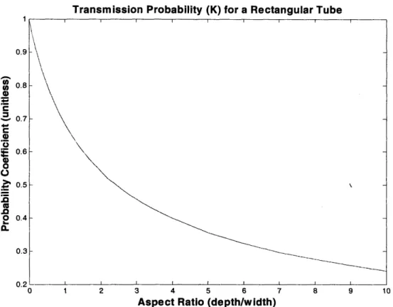
Knudsen transport is the movement of an incident molecule through an orifice without reacting with the side-wall of the orifice. Take a two chamber system connected by an orifice as shown in Figure 2-12. The diffusion of a molecule in chamber 1 with pressure 1 through the orifice into chamber 2 with pressure 2 depends on the pressure and the geometry of the orifice. Knudsen transport states that there is a probability coefficient
K that a molecule will start in chamber 1 and diffuse to chamber 2.
The probability coefficient K completely depends on the geometry of the tube that the molecule transits. The molecule reflects off the sidewall of the tube following a cosine law and there is no sticking on the tube sidewall. In application to plasma etch, K is the molecular transmission probability or likelihood that an incident molecule will reach the trench bottom by diffusion. K is dependent on aspect ratio, and has been empirically tabulated in the literature [17][18]. Figure 2-13 plots the transmission coefficient K as a function of aspect ratio. This model, or variants of this model, will be used in the proposed non-uniformity model discussed in Chapter 7.
Chamber 2
Transmission Probability (K) for a Rectangular Tube 0.5 0.4 0.3 2 .0 1 2 I 4 5 6 7 8
1
2 3 4 5 6 7 8Aspect Ratio (depth/width)
Figure 2-13 - Plot of Knudsen transmission probability, K.
9 10
2.6 Summary
This chapter reviews the relevant theories, terminologies and models used to describe plasma etch non-uniformities, and discusses each of them in terms of wafer-, die-, and feature-level scales which have been designated for our pattern density and aspect ratio dependent based prediction models.
Chapter 3
Mask Description
A test mask is used in this work to understand and characterize pattern dependent
variations in plasma etching. The mask pattern was originally designed to study electro-copper deposition (ECD) and chemical mechanical polishing (CMP) pattern dependencies, using a wide range of feature and density structures. The mask has structures that allow for characterization of the effects of aspect ratio and pattern density on the etch rate of trench lines. The mask further allows for the modeling of the plasma etch process, improving ECD and CMP models, and integrating plasma etch, ECD, and
CMP models.
In this chapter, the mask floor plan and layout is presented in Section 3.1. We then present two set of structures that are used in generating a data set for this thesis. Section
3.2 describes the capacitance structures, while Section 3.3 describes the line width and
space structures. Finally, Section 3.4 concludes the chapter. 3.1 Mask Floor Plan
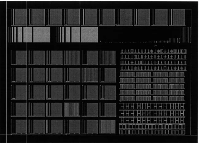
The test mask is 15.1x22.3 millimeters in size and has a floor plan consisting of seven regions: (1) capacitance/comb structures, (2) line width and space (LWS) structures, (3) variable array structures, (4) variable line length structures, (5) dummy fill structures, (6) slotting structures, and (7) near neighbor structures. These structures correspond to the labels listed in Table 3-1.
Table 3-1 - Definition of block names for the Copper Mask.
No. Structure Name Structure Definition
1 Cap_Total capacitance/comb structures
2 CuLineArrayBlock line width and space structures
3 Var_Array_Total variable array structures
4 ISO_varLength_Total variable line length structures
5 DummyBlock dummy fill structures
6 SlotBlock slotting structures
7 Iso Line_$_Boxsand Total near neighbor structures
The nomenclature for line width and space structures and capacitance structures are as shown in Table 3-2. The line width and space structures, along with the capacitance structures, are the most relevant in our research to determine pattern dependent effects caused by plasma etching. The other structures are useful for verification and extension of our etch model and models (ECD and CMP) that predict copper metallization variations.
Table 3-2 - Nomenclature for individual Capacitance and Line Width and Space blocks.
Structure Name Structure Definition
BlockLinelw0_l1s0_27 Line Width/Space of 0.1 and 0.27 micron, respectively BlockLinelw31sl Line Width/Space of 3 and 1 micron, respectively CapCombo$LW_0_OLS_6$LW_5LS_5 Two Capacitance Structures: Line Width/Space of 0.1/6
and 5/5 microns
CapCombo$LW_6LS_0_8$LW_0_5LS_I Two Capacitance Structures: Line Width/Space of 6/0.8
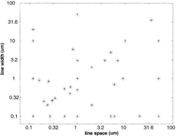
1 1and 0.5/1 microns c cures .1/.27 .21.24 .1/.54 1/9 .1/1 /55 .26/.3 3/7 .85/.25 10/10 .3/.34 0.1/6 5/5 0.1/0.12 0.2/2 6.01.8 0.5/1 1/1 3T3.8 0.25/0.2 0.7/6
Figure 3-1 - Schematic of copper mask along with line widths and line spaces for each capacitance and line width and space structure (in pm).
6/.8 .4L.7 35/35 1/1 50/1 .1/20 .54/.54 10/.12 3/1 1/.12 2/2 .1 /12 .6/.72 20/.12 .91.16 10/50 .1/.27 .11.54 .2/.24
100 31.6 10 3.2 1 0.32 0.1 0.1 0.1
Figure 3-2 - The design
0.32 1 3.2 10 31.6
line space (um)
space of line widths and spaces encompassed by the and line width and space structures.
The various line width and line space combinations for the capacitance and line width and space structures are shown in Figure 3-1. The layout design space spanned by the two regions is mapped in Figure 3-2. Figure 3-3 illustrates the layout of the capacitance and line width and space structures on test mask.
100
Figure 3-3 - Test mask layout.
3.2 Capacitance/Comb Structures
Capacitance or comb structures are designed for post-metallization electrical measurements for the study of ECD and CMP process induced variations. For our etch variation studies, these capacitance structures also provide post-etch measurement data for studying etch process non-uniformity. Capacitance structures form arrays of trench lines as illustrated in Figure 3-4. Capacitance structures are indexed from CA1 to CA10, left to right, as shown in Figure 3-4.
I I
Figure 3-4 - Capacitance structures.
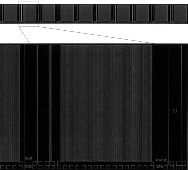
3.3 Line Width Line Space Structures
There are thirty LW/LS structures arranged in an asymmetric assortment of pattern densities and pitches. These structures, along with the capacitance structures, are used to characterize the dependence of etch rate, depth, critical dimension, and line space on
Figure 3-5 - Line width and space structures.
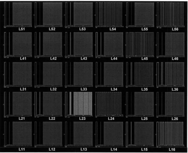
These LWS structures are also used in modeling etch rate and CD profile. They are in a row and column arrangement with each structure given identified with an L, followed by the row and column numbers as shown in Figure 3-5. The asymmetric arrangement of the structures allows for the interaction of neighboring structures with different pattern densities. This interaction affects the microloading of individual trenches which are in competition for reactants as explained in Chapter 6. We are also able to examine and understand the transition from a high density region to a low density region by examining trench lines of adjacent structures with high and low densities, respectively.
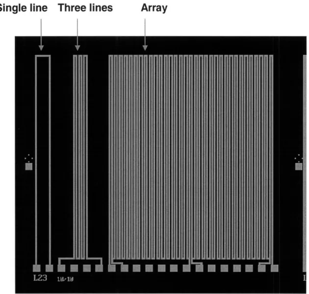
Single line Three lines
I
I
Figure 3-6 - Close up view of a line width and space module with line width and line space of 10 pm and density of 50%.
Each module consists of (1) an isolated line, (2) an isolated serpentine line, and (3) an array of serpentine lines (Figure 3-6). The isolated line is a single line that goes up and bends back down. The isolated serpentine line is also a single line that goes up and bends down three times. The array is composed of many trench lines that are connected as shown in Figure 3-6. For each LWS module, all three parts of the module fit in a 1919 jm x 1702 Im region. Table 3-3 gives the specification for all the modules, including the
local pattern density, the targeted etch depth, and the resulting targeted feature level aspect ratio.
Table 3-3 - Specifications for each line width and space structure.
Module Line Name Width (in pm) L51 0.1 L52 0.1 L53 0.1 L54 0.1 L55 0.2 L56 1 L41 3 L42 1 L43 3 L44 6 L45 50 L46 0.6 L31 1 L32 0.1 L33 0.85 L34 0.4 L35 0.1 L36 20 L21 2 L22 5 L23 10 L24 35 L25 0.54 L26 0.9 LII 0.1 L12 0.26 L13 0.3 L14 1 L15 10 L16 10 Line Space (in Am) 0.27 0.54 5 50 0.24 50 1 9 7 0.8 1 0.72 0.12 1 0.25 0.7 20 0.12 2 5 10 35 0.54 0.16 0.12 0.3 0.34 1 0.12 50 Pitch (in Am) 0.37 0.64 5.1 50.1 0.44 51 4 10 10 6.8 51 1.32 1.12 1.1 1.1 1.1 20.1 20.12 4 10 20 70 1.08 1.06 0.22 0.56 0.64 2 10.12 60 Line Length (in Am) 1604 1604 1604 1604 1604 1604 1604 1604 1604 1604 1604 1604 1604 1604 1604 1604 1604 1604 1604 1604 1604 1604 1604 1604 1604 1604 1604 1604 1604 1604 Targeted Targeted Density Depth (in Am) 0.27027027 0.27 0.15625 0.27 0.01960784 0.27 0.00199601 0.27 0.45454545 0.27 0.01960784 0.27 0.75 0.27 0.1 0.27 0.3 0.27 0.88235294 0.27 0.98039216 0.27 0.45454545 0.27 0.89285714 0.27 0.09090909 0.27 0.77272727 0.27 0.36363636 0.27 0.00497512 0.27 0.99403579 0.27 0.5 0.27 0.5 0.27 0.5 0.27 0.5 0.27 0.5 0.27 0.8490566 0.27 0.45454545 0.27 0.46428571 0.27 0.46875 0.27 0.5 0.27 0.98814229 0.27 0.16666667 0.27 Aspect Ratio 2.7 2.7 2.7 2.7 1.35 0.27 0.09 0.27 0.09 0.045 0.0054 0.45 0.27 2.7 0.317647059 0.675 2.7 0.0135 0.135 0.054 0.027 0.007714286 0.5 0.3 2.7 1.038461538 0.9 0.27 0.027 0.027 3.4 Summary
The copper mask is used to characterize and model the effect of line width and pattern density on etch rate. The capacitance and line width and space structures allow for characterizing and modeling etch rates, while the rest of the structures can be used to verify and extend the model.
![Figure 2-1 - Profile of plasma etching non-uniformity causes and effects [7].](https://thumb-eu.123doks.com/thumbv2/123doknet/14234495.485991/17.918.141.780.201.691/figure-profile-plasma-etching-non-uniformity-causes-effects.webp)
![Figure 2-8 - (a) Global etch map for 0.06% loading, which features a hot spot at the middle left part of the wafer [12]](https://thumb-eu.123doks.com/thumbv2/123doknet/14234495.485991/30.918.146.762.185.506/figure-global-etch-loading-features-spot-middle-wafer.webp)