DOCUTEN
ROOM 36-412i
ANALYSIS OF CIRCUITS WITH MULTIPLE-HOLE
MAGNETIC CORES
LUBOMYR S. ONYSHKEVYCH
TECHNICAL REPORT 329
JULY 9, 1957
MASSACHUSETTS INSTITUTE OF TECHNOLOGY
RESEARCH LABORATORY OF ELECTRONICS
CAMBRIDGE, MASSACHUSETTS
____·· I..XI__I___I·.l_ I·I.I1_ ··I1 -.
a
The Research Laboratory of Electronics is an interdepartmental laboratory of the Department of Electrical Engineering and the Department of Physics.
The research reported in this document was made possible in part by support extended the Massachusetts Institute of Technology, Research Laboratory of Electronics, jointly by the U. S. Army (Sig-nal Corps), the U. S. Navy (Office of Naval Research), and the U. S. Air Force (Office of Scientific Research, Air Research and Develop-ment Command), under Signal Corps Contract DA36-039-sc-64637, Department of the Army Task 3-99-06-108 and Project 3-99-00-100.
MASSACHUSETTS
INSTITUTE OF TECHNOLOGY
RESEARCH LABORATORY OF ELECTRONICS
Technical Report 329
July 9, 1957
ANALYSIS OF CIRCUITS WITH MULTIPLE-HOLE MAGNETIC CORES
Lubomyr S. Onyshkevych
The work presented in this report was submitted as a thesis in partial
fulfillment of the requirements for the degree of Master of Science,
Department of Electrical Engineering, M. I. T., June 1957.
Abstract
Multiple-hole magnetic cores, also called transfluxors, which have been developed
recently, promise to be very useful in computer, control, and other logical circuitry.
They are ferrite cores, with square hysteresis loops, of various complicated
geom-etries.
In this report, a workable analysis procedure for circuits that contain transfluxors
is developed; it is based on the square-waveshape approximation.
This analysis forms
a basis for a design procedure. Sample circuits were designed and tested, and the
results were found to be within 10 per cent of the predicted values.
The main problems in circuit design were flux division and loading effects. Diode
elimination presented another problem, which is treated at some length in this report.
Diodeless operation of a transfluxor circuit was found to be possible, but slow,
unreli-able, and critical.
In the field of logical design, a symbolic notation was developed, and an approach
to design was made, using "gate boxes."
A description of the physical properties of transfluxors is given; it includes some
new, unpublished, special effects encountered with multiple-hole cores.
Table of Contents
Introduction
1
1. 1 History
1
1.2 Objectives
2
1.3 Experimental Setup
2
II.
Physical Properties of Multiple-Hole Cores
5
2. 1 Introduction
5
2.1.1 Domains
5
2.1.2 Ferrites
6
2.2 Behavior of a Simple Core
6
2.2.1 Hysteresis Loop
6
2. 2.2 Voltage Waveform
9
2.2.3 Switching Characteristics
10
2. 2.4 Undesirable Voltages
11
2.3 Behavior of an Idealized Transfluxor
11
2.3. 1 Basic Operation
11
2.3.2 Switching Mechanism
12
2.3.3 Inherent Time Delay
14
2.4 Flux Distribution
16
2.4. 1 General Principles
16
2.4.2 Ambiguities
17
2.5 Nonideal Behavior of Transfluxors
17
2.5. 1 Switching
17
2.5.2 Effect of Loading
19
2.5.3 Noise
19
2.5.4 "Near Leg" Effect
19
III.
The Logical Properties of Multiple-Hole Cores
23
3. 1 Introduction
23
3.2 Schematic Notation
23
3.3 Problems of Logical Design with Multiple-Hole Cores
25
3.3.1 General Approach
25
3.3.2 Modes of Operation
25
3.3.3 Diode Elimination
26
3.3.4 Gate Boxes
28
3.3.5 Limitations and Precautions
29
3.4 An Example: The Five-Hole Transfluxor
30
3.4. 1 Modes of Operation
31
3.4.2 A Sample Circuit
31
3.5 Extension of the Principles Derived to More Complicated
Geometries
34
IV. Analysis and Design of Circuits with Multiple-Hole Cores 35
4. 1 Introduction 35
4. 1. 1 Approximate Analysis of Circuits with Simple Cores 35
4. 1. 2 New Problems Arising with Multiple-Hole Circuits 38
4. 2 Approximate Methods of Dealing with Multiple-Hole Circuits 38
4.2.1 General Considerations 38
4. 2.2 Flux Division and Loading Effects 39
4.2.3 Equivalent Circuit 42
4.2.4 Design and Blocking Pulses 45
4.3 Examples of Design 46
4.3. 1 Diodeless Shifting Register 47
4.3.2 Accumulator 47
4.4 Experimental Results 47
4.4. 1 Results of Operation 47
4. 4. 2 Explanation of Discrepancies Between the Theoretical
and Experimental Results 49
V. Conclusions 50
5.1 Summary 50
5. 1.1 Problems Studied 50
5. 1. 2 Conclusions Reached 50
5.2 Suggestions for Future Research 51
Appendix A Relationship Between R and Ro 53
Appendix B Flux Division for Semisinusoidal Voltage Waveform 55
Appendix C The Design of the Diodeless Shift Register 56
Appendix D Design of the Accumulator 59
Acknowledgment 60
Bibliography 61
I. INTRODUCTION
1. 1 History
In recent years, a great deal of work has been done in the field of ferromagnetism.
Numerous devices and new magnetic materials have been developed and perfected.
Among the most important are the square-loop materials; that is, materials that have
an approximately rectangular hysteresis loop (40). Two kinds of magnetic material that
can be made to exhibit this desirable property are in general use: tape-wound,
thin-metal cores and ferrites (39, 45).
Currently, a new material - thin film - is being
developed (46).
Many applications of square-loop materials have been found in the field of computing
and control.
The development has taken two directions: magnetic amplifiers (22, 23, 24)
(circuits using a carrier frequency) and pulse applications (circuits using pulses and no
carrier). Only pulse circuitry is discussed in this report.
The first applications of magnetic pulse circuitry were made in the field of
informa-tion storage.
Magnetic shift registers (26, 27, 28) and huge magnetic-core memory
matrices (30, 34, 35) have been developed and are being used in most modern computers.
Here, the trend is towards bigger, faster, cheaper memories, with the result that new
magnetic storage elements are constantly being announced (31, 37).
Notable among them
is the multiple-aperture ferrite plate (36, 32).
Also, much work has been done on logical-circuitry applications of magnetic cores
(19, 16, 20, 15).
The object was to develop various logical gating circuits, as well as
complete arithmetic units for computers and similar devices. In this area, the efforts
were less successful; magnetic cores require coupling diodes and high-current drivers,
and are not particularly fast. It was evident that if applications of magnetic cores were
to become practical, new kinds of magnetic elements would have to be developed.
Until 1955, the magnetic cores in use were of simple toroidal shape. Then Rajchman
of the RCA Laboratories announced a new kind of magnetic core, the Transfluxor (7, 8),
which was basically a multiple-hole magnetic core made out of ferrite. This core could
do anything that the simple cores could do (for example, in many instances, a single
transfluxor could be used in place of several toroidal cores), and it permitted new
applications. It could be used as an analog device, operating like a magnetic
ampli-fier with electrically controllable magnetic setting. Also, it could be used as a
com-plicated gate and, therefore, offered the possibility of eliminating diodes from logical
magnetic circuitry.
Since that time, investigation on complicated core geometries has been undertaken
by various groups; many interesting facts have been uncovered, and useful devices
designed.
The Potter Instrument Company has designed "Magnistors," which use both
square-loop material and soft iron in the same core (6); International Business Machines
Corporation has developed four-legged memory cores (4, 5); the General Electric
Company has done some very interesting transfluxor research (1, 3); and new facts also
have been forthcoming from Radio Corporation of America, notably the principle of cur-rent steering (9). In addition, some work on multiple-hole cores has been done in other countries, especially Germany (Z). Work on multiple-hole cores has also been going on at the Research Laboratory of Electronics, M. I. T.; this report describes the first results of this work.
1. Z2 Objectives
The primary objective of the research undertaken for this study was the development of a method of analysis of logical circuits containing magnetic cores with complicated geometries. It is hoped that from this work a method of synthesis will ultimately result - one that will make possible simple design procedures of large logical systems con-sisting of such cores. Only logical circuits (including shift registers) are considered; the investigations reported here concern pulse-type application (no carrier) exclusively, and binary digital applications are of prime importance.
In order to understand better the behavior of transfluxors and transfluxor-like devices as circuit components, an investigation into the properties of the core itself was undertaken. In the course of this research, many new facts were brought to light, and theories about them were formulated. Some of those facts have, in the meantime, been discovered and reported by others; some are entirely new. A discussion of all of them and a general background discussion of magnetic cores comprise the second section of this report.
The third section is concerned with the logical design and analysis of multiple-hole magnetic-core circuits, especially with the development of a symbolic system of nota-tion. An attempt to summarize the logical functions obtainable from a few particularly useful forms is also included.
In the fourth section, the knowledge gained from investigation of the properties of transfluxors is utilized to formulate an approximate method of analysis of transfluxor circuits. From this analysis, a design procedure is deduced; sample circuits have been designed and physically tested on the basis of this procedure. The experimental results are compared with expected behavior. An attempt to account for the discrepancies between theory and practice concludes the section.
The fifth section summarizes the results and suggests the paths that, in the opinion of the author, should be pursued in future investigation.
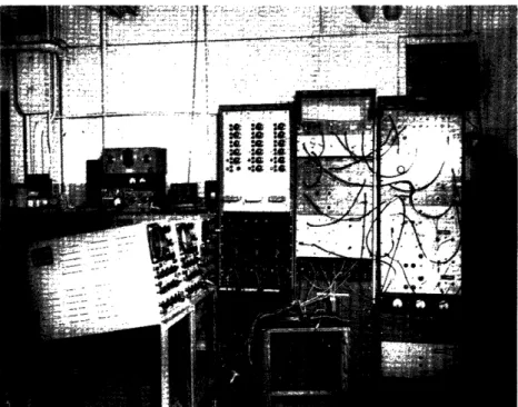
1.3 Experimental Setup
Many different kinds of cores were used in this research, including both simple toroidal and complicated multiple-hole cores. Some of them are illustrated in Figs. 1 and 2. Multiple-hole cores either were obtained directly from RCA or IBM, in which case they were of formed and sintered ferrite, or were drilled with a supersonic drill from blanks obtained from the M. I. T. Lincoln Laboratory.
The cores were tested statically on the static hysteresis curve plotter at the M. I. T.
f O
O
.O
00
0
If I11 '*~0
I
!..>/lltt; e ef e s e t : I I - aFig. 1.
Some of the cores used in
this investigation.
Fig. 2. Examples of wired cores.
Fig. 3. Experimental setup.
Insulation Research Laboratory as well as dynamically with trains of sharp high-current pulses obtained from the flexible experimental setup assembled and partially built at the Research Laboratory of Electronics. This setup was also used to test complete circuits _ and for many other purposes. Figure 3 shows the pulse equipment used.
II.
PHYSICAL PROPERTIES OF MULTIPLE-HOLE CORES
2. 1 Introduction
At the present time, no adequate quantitative theory of physical behavior of a simple
core during switching conditions exists, and there is virtually no theory of behavior of
multiple-hole cores. In this section, the behavior of the transfluxor, its special effects,
and modes of operation are discussed qualitatively.
A brief explanation of a simple core
is first necessary.
2. 1. 1 Domains
According to the domain theory of magnetism (38, 41, 42, 43), a ferromagnetic
mate-rial contains magnetic dipoles that result from unbalanced electron spins. In a small
region of the ferromagnetic material, all of the dipoles are parallel and held aligned in
the same direction.
The forces that hold them in alignment are very powerful, but as
yet not completely understood.
The small region of the ferromagnetic material is called a "domain." Each domain
is completely magnetized in some direction at all times because all of the magnetic
moments are both parallel and in the same sense. However, in some materials, some
of the dipoles are antiparallel; such a material is termed "ferrimagnetic." If, in a
)
B
(a) (b)
Fig. 4. Domains and switching.
(a) Magnetic material consisting of two domains;
rho1 o _rwhrf loft_hn--1 A-mnn 4 i- r
luy :-.L:U . ZZ4,C:J.,,.., D.
(c) all material in left-hand domain after switching by field B;
(d) further magnetization possible only by rotation of flux direction inside the
UULLd.ii
(c) (d) ke 4 I J 1 i -'e /'t1IO 1 V U1 UA t 1 idL1 I I u, )
domain returns to preferred direction
of magnetization and is now in
magnet-ized state.
(e)5
·f 1" , VLIZLLII f;-L' A 1LLQI L .~~ aI uu111CLIiil I- % __ _ _ ___j , _C .,1 -,,^ferrimagnetic material, all of the antiparallel dipoles exactly balance each other, so that
each domain has no net magnetic moment, we term the material "antiferromagnetic."
In a crystalline material, there is usually a preferred direction of magnetization
along some crystal axis; this is called "crystalline anisotropy." There can be more than
-one preferred direction.
Moreover, in a polycrystalline material, the crystals
them-selves can be oriented randomly so that, as a whole, the material may be nonoriented,
even though each domain is anisotropic.
Domains are separated by the so-called "domain walls" or "Bloch walls," which are
several hundred atoms thick. The walls can move, making one domain larger at the
expense of other domains.
(See Fig. 4.)
Figure 4 shows a simple explanation of magnetization of a ferromagnetic material.
The idea to bear in mind is that, even though each domain is always completely
"satu-rated," the specimen as a whole may be demagnetized because all of the disoriented
fields of the individual domains cancel each other.
2. 1.2 Ferrites
All of the multiple-hole cores used in this investigation, as well as most of the
toroidal cores, were ferrite (44).
Ferrite (45) is a ferrimagnetic (48) ceramic material
with the general chemical formula:
M2+ 0 · M3+
where the metal M can be iron, nickel, zinc, manganese, or magnesium, in various
proportions.
By choosing the proportions of metals correctly, as well as by firing the
core in the correct way, the desired characteristic properties of the material can be
obtained.
For square-loop applications, the ferrites are usually of the MgMn type (45).
2. 2 Behavior of a Simple Core
2.2. 1 Hysteresis Loop
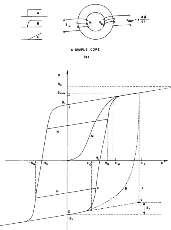
An idealized hysteresis loop is shown in Fig. 5b.
To obtain this loop the core is
wired as shown in Fig. 5a.
A current is applied on winding N
1, and the voltage across
winding N
2is observed.
From these measurements, we can compute the variables H
and B at the time T because
N1 [ampere-turns(
H [oersteds] = 0. 495 N1
ie-trnsh
J(1)
while
7
dt
volt-seconds
B [gauss]
1. 550 X A
Lturns-inc
nds
(2)
6
I
A,Li
A SIMPLE CORE (a) B B, B max Br HN Hw I A I Bn -BrIDEALIZED HYSTERESIS LOOP (b)
Fig. 5. Switching of a simple core.
7
dt
where
N1 = number of turns in winding N1
N = number of turns in winding N2
I = applied current L = length of path, inches A = cross-section area, inch2
v = output voltage
Ampere-turns and volt-seconds often are used as units of measurement instead of oersteds and gauss.
If the core is completely demagnetized, and then a positive H-field is applied, we travel along the initial magnetization curve M until saturation is reached. When the
current is released, the flux will return to the remanent flux Br . Arbitrarily, we can
assign to this point state the number "1 ". If we now apply a current of opposite polarity, the core will switch into the negative saturation -Br, and after the release of current
stay in the state "0". Thus we have achieved a memory - a bistable device. The core can be switched back and forth between states 1 and 0, provided, of course, that the applied H-field is large enough to cause saturation in each direction. If it is not, then the magnetization may follow some minor hysteresis loop like the one marked "N" in Fig. 5b. If the H-field is not large enough to force the magnetization over the knee of the hysteresis loop (Ho), no switching at all will result. Thus the "coercive force" HC gives some indication of the amount of current to be employed.
The core takes a finite amount of time to switch from state to state. Therefore, if we employ a sharp, fast pulse, the core is not able to follow instantaneously. Therefore, we actually never switch along the hysteresis loop C, called the "static loop," unless the current is applied in the form of a very slow, almost dc ramp. At the other extreme is a current step that causes the core to go along path A. In between we get paths like B, which are normally caused by steps with finite, but fast, rise times.
The ratio B
s =Br
(3)
B
is called the "squareness ratio" and is a figure of merit of the material; for a good, square loop, it should be of the order of magnitude of 0. 9 - 0. 95. Another definition of squareness ratio is:
B max
s max (4)
B r
where Bmax corresponds to Hp = ZHC . This is a much more useful definition.
8
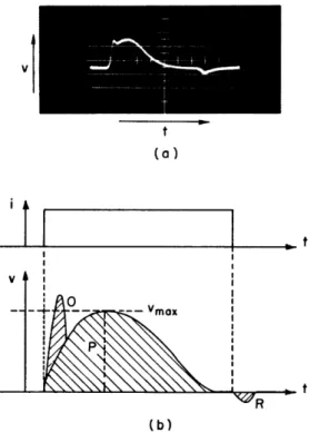
2. 2. Z2 Voltage Waveform
While the core is being switched from one remanent state to the other, a voltage d~
v = k-t (5)
appears across the winding N2. The waveshape of this voltage is shown in Fig. 6a.
There is no good quantitative explanation of this waveshape; qualitatively, we can explain it (see Fig. 6b) as follows. [This explanation is due to H. K. Rising, and also to W. M. Breckenridge (13).]
Let us suppose that the core was originally in state O and that we applied a sharp current step that tended to reverse the core. The domain walls cannot move instantane-ously; we follow path A in Fig. 5b, as explained previously. In this region, magnetiza-tion is caused by initial rotamagnetiza-tion of domains, which is much faster than wall movement.
Thus in a very short time, point X is reached, causing a change in flux Bn. This causes the sharp spike at the beginning of the voltage waveform, labeled "O" in Fig. 6b. After-wards, correct switching of the core produces the bulk of the waveform P. The peak of this part of the waveform is reached when the H axis is crossed. Obviously, the voltage waveform is asymmetrical.
After the current is released, the flux falls to Br at the "1" point (Fig. 5b). A negative voltage spike R occurs, which has an area proportional to B ma-Br
If the applied Hp is very much larger than HC, parts O and P come closer and
I
t (a) -__ ' t V- : (b)Fig. 6.
Switching waveform.
9
iI k
V t (b) V t
(c)
/ NImin NI (a) NImin NI (b)Fig. 7. Switching waveform at various
values of switching current.
(a) IN = 1.2 ampere turns;
(b) IN = 1. 6 ampere turns;
(c) IN = 2.0 ampere turns.
Fig. 8. Switching characteristics.
(a) Inverse of switching time vs. ampere turns;
(b) peak voltage/turn vs. ampere turns.
closer together and finally merge, as seen in Fig. 7.
2. 2. 3 Switching Characteristics
The net area of the voltage waveform remains of the ampere-turns applied, provided the core is inverse of the switching time and the peak voltage mmf (26, 13), as shown in Fig. 8. Thus
constant and equal to
switched completely.
vary almost linearly
A~, regardless However, the with the applied
1 T =
K
(NI - NImin) s vN=
Kz(NI -Nmin )(6)
(7)
The slope of the v/N vs. NI characteristic, called Ro, will be very useful later in the design procedure, as will K, the slope of the 1/Ts vs. IN characteristic.
Note that both NImin (which corresponds to HW and is close to, but not the same as, HC) and HC depend upon the length of path around which the switching is supposed
to occur. Thus both NImin and HC are lower for a toroid of small circumference than are the corresponding parameters for a core of large circumference, the material and
10
vl
t (a) I/T., Vmox N---cross-section area being the same for both cores.
Z. Z. 4 Undesirable Voltages
The spikes at the beginning and at the end of the voltage waveform are undesirable, but are usually not particularly objectionable in pulse
TxrkrL HT~~xnwovr anot-he]- r lta p fhe -called 11 V V . - VV V -r
s
J -V -L v b.e _ _ I W-"zero" output, is extremely undesirable. This volt-age occurs when we try to pulse the core in the same direction in which it is already set. Under this con-dition, a complete absence of output would be
prefer-t
able, but we get a voltage, as shown in Fig. 9, that
corresponds to the flux value B max - B .r (The net
Fig. 9.
Zero-one ratio.
volt-time area is still zero.)
The ratio of this "zero" voltage and a full "one"
output (due to switching of the core by the same current) is called the zero-one ratio; it
is proportional to the squareness ratio and is often employed in testing cores.
2. 3 Behavior of an Idealized Transfluxor
Most of the basic ideas about transfluxor operation can be explained by considering
a two-hole core, as shown in Fig. 10a.
Let us go through a basic sequence of operations
that apply to the core pulses, as shown in Fig. 10b.
2. 3. 1 Basic Operation
In our basic sequence, we first apply a pulse to the winding labeled "block," which
saturates the whole core completely in the clockwise direction, as shown in Fig. 10c.
Then we apply a pulse to the "unblock" winding, which tends to switch the flux in the
counter-clockwise sense. Let us suppose that the applied mmf is strong enough to switch
the flux along the shorter path a, but not strong enough to cause flux reversal along the
longer path
.
We get a flux distribution like that shown in Fig. 10d. Notice that we
have, effectively, a closed loop around the small hole (shown with a dotted line in
Fig. 10d, with the result that if a pulse is applied to the "drive" winding we can reverse
the flux around the small hole and get an output on the output winding.
We now have a
flux distribution like that shown in Fig. 10e and, therefore, can switch the flux around
the small hole back and forth, producing positive and negative voltage pulses at the
"out-put" winding, forever after.
If the "unblock" pulse were missing, the core would still be in the state shown in
Fig. 10c when the "drive" pulse arrived, so that switching around the small hole would
be impossible. If the "drive" pulse were big enough, we could still switch around the
big hole. [This is called "spurious unblocking" (8).] Thus, if we want to have a gate, we
must apply a "drive" pulse of the correct magnitude, that is, big enough to switch around
11
V
PUT ALTERNAT DRIVE I'BLOCK
t
'UNBLOCK IDRIVE UNBLOCKCROSS- SECTION AREAS Ai+A2< A3
(a) (b)
AFTER THE AFTER THE BLOCK PULSE UNBLOCK PULSE
(c) (d)
Fig. 10. Two-hole transfluxor.
the small hole, but not big enough to reverse the flux around the large one.
Instead of driving the core on the outer leg, we could apply a "drive" pulse on the
inner leg, driving through the winding labeled "alternate drive." Now there is no
possi-bility at all of unblocking the core at time 3 because the "alternate drive" tries to switch
the core in the direction in which it is already set; thus, there is now no maximum limit
on the driving pulse.
We see that the transfluxor can act as a gate that can be closed or opened by a single
pulse.
In Sec. III, we discuss many other elementary building blocks that are
realiz-able with this and other forms of multiple-hole cores.
2. 3.2 Switching Mechanism
In the previous discussion, it was assumed that we can actually reverse flux a, but
not flux
, by applying an appropriate "unblock" pulse (see Fig. 10). In other words,
we want exactly one half of the flux reversed - the half that is nearer to the center of
the core.
The real transfluxor does not behave exactly in this way, but we can discuss
12
2 3L
AFTER THE DRIVE PULSE (e) I I i iI I--- - --
---I t t t OLvcrxBLOCKED PARTIALLY OPTIMALLY
UNBLOCKED UNBLOCKED
(a) (b) (c)
OVER- UNBLOCKED COMPLETELY REVERSED
(d) (e)
Fig. 11. Switching of a transfluxor.
first an idealized model that does.
This idealized model is similar to the explanation
of transfluxor behavior published by Rajchman (7, 8).
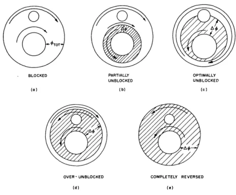
Let us first imagine that the whole transfluxor consists of one single domain that is
magnetized by the blocking pulse in a clockwise direction, as seen in Fig. 1 la. If we
apply an unblocking pulse to the core in the form of a slow ramp current, the NImin
will be reached first in the part of the core that has the shortest path, that is, the part
nearest the middle hole.
Thus, another domain of counterclockwise saturation begins
to grow outward from the center hole, as shown by parts b through e of Fig. 11.
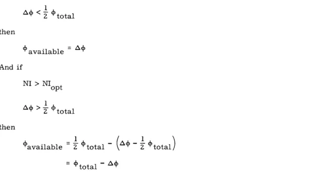
Obviously there is a point at which we have an optimal condition, that is,
when
exactly one half of the flux is reversed; or, in the notation of Fig. 11, when
1
A 2
total
(8)
At this point we have the maximum available flux for switching around the small hole,
as seen in Fig. 12:
1
qavailable max
2
total
(9)
For this, the applied ampere-turns must be
NI = NIopt
(10)
If the reversed flux is smaller, that is, if
NI < NIop
t(11)
13
< tota (12)
then
available
(13)
And if
NI > NIopt
(14)
1
A >
2
4'total
(15)
then
bavailable
2 f total
(
-2
total)
(16)
= total -A
From these considerations we get the curve of Fig. 12.
It is surprising that, even though the real transfluxor does not behave exactly in the
same way as our idealized core (7, 8), we still get a characteristic very similar to that
of Fig. 12.
This fact suggests the use of transfluxors as analog devices, perhaps as
"magnetic gates with a variable magnetic setting" (8).
This application, however, is
outside the scope of this report.
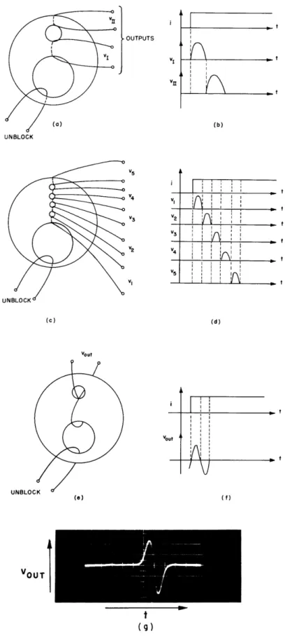
2. 3.3 Inherent Time Delay
The transfluxor will function in the way described in the preceding section even when
we apply a sharp step instead of a ramp.
(This statement is idealized and will be
modi-fied in later discussion.) In other words, the switching starts near the center and
prop-agates outward.
This propagation is stopped at any point either by terminating the
current pulse in time or by limiting its amplitude.
It is evident that if we wire the transfluxor at the inner and outer leg of the small
hole, as seen in Fig. 13a, we shall get a pickup first at the inner leg and then at the
outer leg. See Fig. 13b.
This principle can be utilized to obtain fixed delay by using a
,AVAILABLE
AVAILABLE MAX -2 'TOTAL
N I
NiOPT
Fig. 12.
Flux available for switching around the small
hole as a function of unblocking ampere turns.
14
·_
A - I 'k
VI ,12 (b) v5 V4 v3 V2 (c) Vout VC (e) (d) , , I , Ut I ( f) VOUT
t
(9)Fig. 13. Inherent time delay.
15 I
i
t t IRI nl' V'·YLVY·\multiple-hole core, as seen in Fig. 13c and d.
The principle of time delay can best be verified experimentally by winding the core
as shown in Fig. 13e, that is, by winding the outputs on the inner and outer loops in
oppo-sition. The predicted output of Fig. 13f matches the experimental result of Fig. 13g.
The principle of time delay was actually used by Goldner (3) to obtain many staggered
pulse times; the principle was also discovered and studied independently by this author.
The real transfluxor does not behave exactly in the way our idealized core would behave.
Instead, some overlap occurs between the voltage outputs in Fig. 13b and d, showing
that the outer legs begin to switch even before the inner ones finish.
These overlaps
increase with loading (3).
2. 4 Flux Distribution
The motion of domain walls in a polycrystalline ferrite is extremely complicated.
Therefore, exact flux distribution pictures cannot be obtained by the direct methods in
use (powder method, colloidal-suspension method, etc.). The pictures taken by those
methods have proved to be completely meaningless. Until a more powerful method is
found, we have to be satisfied with voltage measurements, which indicate only the net
change in flux across a given cross section. Moreover we cannot introduce extra holes
for measuring purposes because each hole distorts the flux picture.
2. 4. 1 General Principles
In addition to the voltage measurements, we can take advantage of a few general
principles, obtained either from theoretical considerations or from empirical data.
1.
All flux lines inside the core are continuous, closed loops. This is obvious from
the Laplace equation and from the fact that the measurements show the leakage flux to
be virtually nonexistent.
2.
Any flux reversal must occur along a closed loop. Thus, in order to reverse the
flux at any point, there must be a complete loop of either oppositely magnetized or
demagnetized material available for switching.
The net flux change along this loop must
be the same at any point.
The applied mmf must be bigger than Nlmi
nfor that complete
loop. If there is a branch point, the algebraic sum of either b or A
going out from
this point must be equal to zero. These are consequences of statement 1.
3.
An mmf, applied to any leg of the core, that tends to switch the core in the
direc-tion in which it is already set cannot cause a net flux change anywhere in the core. This
is, perhaps, not as obvious as it sounds.
4. In an unloaded core, if there are two paths of unequal lengths, either of which
can be switched at their meeting point, the switching will favor the shorter loop. This
is discussed more thoroughly in Sec. IV.
5.
If there are many different flux distributions possible at the same time, the core
will choose the state of minimum potential energy. This is a general principle of nature.
6.
Any flux distribution derived will be just an approximation to the statistical
aver-age of the fluxes of the small domains.
2. 4. 2 Ambiguities
By using voltage measurements to indicate the changes in flux and the "General
Prin-ciples" of Sec. 2. 4. 1 for guidance, we can obtain a flux pattern for different states and
configurations. Sometimes, however, more than one model is possible, all of the models
being completely equivalent as far as external A
measurements indicate. A classical
example of this is the five-hole transfluxor (see Fig. 14).
If we first block the
trans-fluxor completely, as in Fig. 14a, and then apply an "unblock" pulse to reverse the flux
completely in leg A, flux reversal will occur along the dotted line. According to
volt-age measurements at all possible points of the core, two flux distribution pictures are
equally acceptable; see Fig. 14b and c.
(Because no coupling seems to occur afterwards
among the small holes, we consider the model of Fig. 14c preferable.)
2. 5 Nonideal Behavior of Transfluxors
2. 5. 1 Switching
A real core does not actually switch as indicated in the model of Fig. 11.
There is
no single sharp wall. Instead, the outer leg begins switching even before the inner leg
completes reversal, as we have already noted at the end of Sec. 2. 3. 3. Also, the final
flux distribution after unblocking does not look like that shown in Fig. 15a; rather, an
approximation of it might be similar to that given in Fig. 15b: some flux has already
been reversed in the outer leg, while the inner leg is still not completely switched.
An example of this "flux division effect" is shown in Fig. 15c and d for another kind
of core - the five-hole transfluxor.
(Measurements were taken both by the static
hys-teresis loop plotter and by dynamic pulse measurements.
Both sets of measurements
agree within 5 per cent, which is the experimental error. The percentages in Fig. 15
are from the static measurements.)
This flux division effect is very troublesome in transfluxor circuitry, especially
because it is greatly intensified by loading. It is discussed further in Sec. IV, where
an approximate method of calculation of flux division is introduced. Here, we only note
that it can be thought of as being caused either by a rather wide region of switching
-a kind of "tr-ansition b-and" th-at moves outw-ard from the center - or, -altern-ately, -as
being caused by two walls moving outward at different speeds, one starting from the
center hole, the other from the small hole.
Because nobody as yet seems to have published any convincing evidence to support
either of these hypotheses, or any other one for that matter, we shall not hazard a guess.
Suffice it to say that the real flux distribution in a polycrystalline, multiple-hole core
is infinitely more complex than our simple model would lead us to believe.
This is a
field in which much research is urgently needed.
17
t
(a)
(c) (c)
Fig. 14.
Ambiguities in flux distribution of a five-hole transfluxor.
(a) (b)
2 %
°O( -58 l58%o 58
58%!.p
IOO%V,_
e-8, (PER CENT) SATURATION (PER CENT)
(C) (d)
Fig. 15.
Nonideal switching of transfluxors.
18
__ __
UN.LU~R
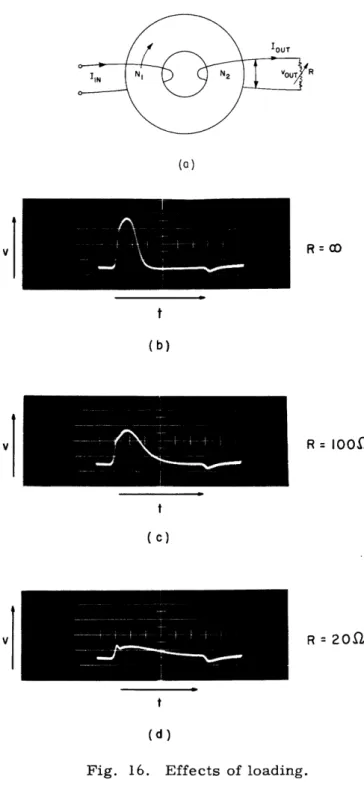
2. 5.2 Effect of Loading
Loading of a core, as in Fig. 16a, by a resistance R has the effects shown in Fig. 16b, c, and d: the switching time gets longer, and voltage amplitude diminishes. This is understandable if we consider that the Iout going through the winding W2
pro-duces a counter mmf, which causes the effective mmf applied around the loop to become: NIeff = Nliin NIout2
This effect is especially important in transfluxors, since not only the speed of switching but also the final flux distribution may depend on loading. For instance, if, in Fig. 15c, we put a heavy load (e. g., a very small resistance) across the winding labeled "sense 3" and applied a large "unblock" pulse, we would get different percentages from those given in Fig. 15c and d. Instead, most of the switching would occur in leg A, since this leg has a much higher NI ff applied to it.
In Sec. IV the effects of loading that were studied are discussed further.
2. 5.3 Noise
There are many sources of noise outputs that can occur in a transfluxor (some of them have already been discussed):
1. Spikes at the time of the beginning and ending of the applied pulse, caused by the slope of the hysteresis loop. This was discussed in Sec. 2. 2. 2.
2. "Zero" output, that is, output occurring when we try to switch the core in the direction in which it is already set (see Sec. 2. 2.4).
3. Outputs caused by the flux division effect, mentioned in Sec. 2. 5.2. This effect is intensified by loading.
4. Outputs due to the "near leg" effect, which are peculiar to transfluxors. A dis-cussion of this phenomenon is given in Sec. 2. 5.4.
Noise outputs 1, 2, and 4 do not correspond to any irreversible change of flux; this means that they do not cause a net change in the volt-time area. This, of course, does not apply to noise output 3.
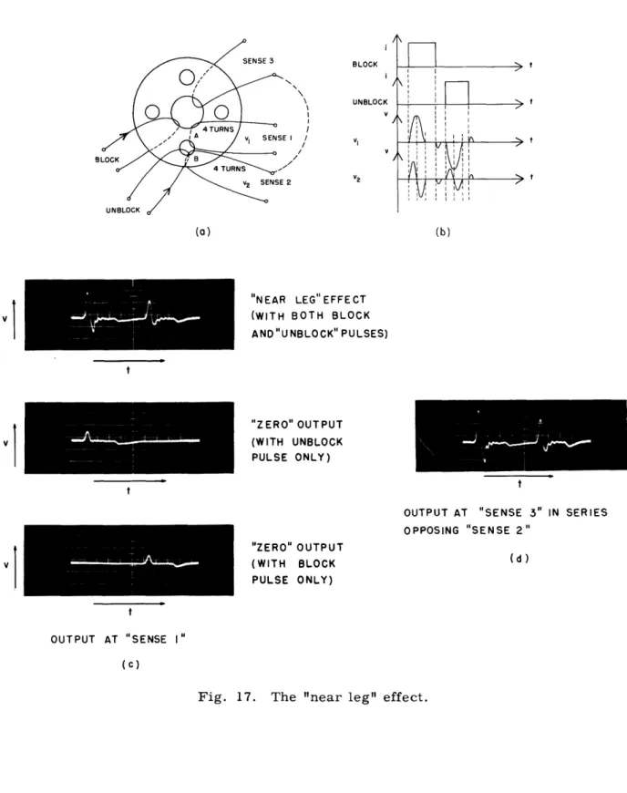
2. 5.4 "Near Leg" Effect
A peculiar transient effect* that occurs in transfluxors is shown in Fig. 17. If we block, unblock, block again, and so on, the core of Fig. 17a by the respective windings, we expect voltages to appear on winding "sense 2," but not on "sense 1," since there is no net flux change occurring in leg A. But, surprisingly enough, we get a consider-able "reversible" voltage, much larger than just the "zero output" voltage, as seen in Fig. 17c.
*
To the author's knowledge, this effect has not been described or mentioned in any paper and was first observed and studied by the author.
tI (a)
vi
t (b) R =IOOS2vi
(C)
R = 202 t (d)Fig. 16.
Effects of loading.
20 V
BLOCK UNBLOCK VI v 2 V2
(a)
"NEAR LEG"EFFECT (WITH BOTH BLOCK AND "U NBLOCK" PULSES)"ZERO" OUTPUT (WITH UNBLOCK PULSE ONLY) "ZERO" OUTPUT (WITH BLOCK PULSE ONLY)
OUTPUT AT "SENSE 3" IN SERIES OPPOSING "SENSE 2"
(d)
OUTPUT AT "SENSE I"
(C)
Fig. 17.
The "near leg" effect.
A
21
(b) t vl t vl I tThis voltage consists of a positive and a negative spike (see Fig. 17b) and looks like the derivative of the pulse on "sense 2." The same effect occurs if legs A and B are interchanged.
One possible explanation of this effect is the following: Let us suppose that the core is in the blocked state and we are applying the unblock pulse. Leg B starts to switch. Because the path around the small hole is so much shorter than the one around the big loop, leg A supersaturates, that is, it moves from state Br towards Bs (see Fig. 5).
Later, when the larger loop has had enough time to begin switching, this supersatura-tion in A has a chance to collapse. This is, in a way, equivalent to saying that the effect is the result of rotation of domains in leg A.
This explanation seems to be supported further by the fact that if we compare (by a series-opposition connection, as shown in Fig. 17a) the voltages on "sense 1" and
"sense 3" windings, we see that the voltage on "sense 3" comes later in time (by a small fraction of the switching time), thus showing that the switching of the whole core does not follow instantaneously the switching of leg B (see Fig. 17d).
No claim is made, however, that this explanation is the "true" one, or that there does not exist another, better explanation of this effect. Further research should clarify this phenomenon.
22
III. THE LOGICAL PROPERTIES OF MULTIPLE-HOLE CORES 3. 1 Introduction
Virtually any logical function expressible in Boolean algebra can be realized with magnetic cores. However, because of the inherent synchronous delay, the magnetic
core is ideally suited to sequential circuit work.
A multiple-hole core can combine the functions of a few simple cores and can per-form some new functions that the simple core cannot perper-form; for example, asynchro-nous time delay.
The first necessity in analyzing logical circuits that consist of any new component is a flexible schematic notation. There are two systems of notation for circuits with simple cores: Karnaugh's mirror notation (16), and the scheme introduced by Loev, Miehle, Paivinen, and Wylen (19). Since there is at present no published schematic notation for multiple-hole cores, a notation was developed as a first step in logical analysis. The basis for this notation is the one developed by Loev, Miehle, Paivinen, and Wylen, but the extension to the transfluxor circuits was made by this author.
3. 2 Schematic Notation
In the proposed notation a multiple-hole core is represented by a set of dots connected by lines to represent the topology of the core. The dots represent holes, and the con-necting lines, the legs between the holes. Dots can be either filled or hollow, to distin-guish between the main and supplementary holes in the core. Figure 18a shows the representation of a five-hole transfluxor.
The inputs and outputs to the core in the form of pulses on windings can go either to a leg between two holes, in which case we represent them as going to or from the line between dots, or to a leg between the outside and a hole, in which case we bring them to the dot itself.
The information flow is represented by a hollow arrow going to or from the core representation for input and output, respectively. Only one pulse is associated with each arrow. If many different pulses flow through the same winding at different times, we draw an arrow for each one of them and connect all of them with a double crossbar. Each arrow has a capital letter associated with it that shows the pulse time at which it conducts information. If the pulse can either occur or not occur, depending upon some information conducted, the letter is enclosed in brackets. A small cross arrow can be used to indicate the direction in which the incoming pulse tries to switch the core (for input pulses), or the direction of switching that produces the given pulse (for outputs). All this is much simpler than it sounds, as can be seen from Fig. 18b. It should be noted that the directions of switching indicated are entirely arbitrary, except that they must be consistent for each core.
The use of colors or different thicknesses of lines is helpful in identifying the core and the connecting lines, especially in complicated circuit diagrams.
23
(a) SET AT TIME B JIPUI AI IIMt A AND B )N DITIONAL) Ir1 PULSE AT TIME A (b) (CONDITIONAL) "B (c)
Fig. 18. Schematic representation of multiple-hole cores. (Note: a "conditional"
pulse is one that may be either present or not, depending on the
informa-tion conveyed.)
Other helpful symbols include: filled arrow without associated letters for a dc
(biasing) winding; a diode-like symbol for diode; a hollow square for a loading resistor.
If the same pulse is either taken from or goes to more than one place on the same core
or on a different core, we indicate that by simply branching the arrow line in question.
It is also helpful to indicate by a double-headed arrow a pulse that is normally big enough
to override either an opposing dc bias or another pulse input that is coincident and
opposing.
This principle can be extended to multiple-headed arrows. Also an oblique
cross can be drawn across an undesirable information flow arrow (see Fig. 18b); this
and some of the other conventions are illustrated in Fig. 18c.
This system of notation was used extensively in the present investigation and, on the
whole, was found to be very satisfactory.
It is simple, easy to understand and to learn,
and it conveys all of the pertinent information.
24
_
3.3 Problems of Logical Design with Multiple-Hole Cores 3. 3. 1 General Approach
In the logical design of transfluxor circuits either of two approaches can be followed: (1) design the cores in order to realize our particular circuit; or (2) design circuits using a standard core throughout the system.
The second method was used in our investigation, since there were no easily avail-able facilities for fabrication of special cores.
The following steps in design procedure were found to be most fruitful:
1. Investigation of the given core geometry and listing of all possible modes of operation.
2. Elimination of the less desirable modes, then placement of the remaining modes in a list of standard "gate boxes" with all pertinent information.
3. Design of the circuit, by means of the well-known switching circuit methods, in terms of the standard gate boxes.
4. Substitution of cores for gate boxes. 5. Final circuit design (see Sec. IV).
3.3.2 Modes of Operation
In classifying the modes of operation for a given transfluxor, care should be taken to notice the following:
CORE A
INPUT G CORE B
LOOP
Bi
Fig. 19. Basic forms of transfer loops.
SHIFT
Fig.
(a) "Variable transformer" coupling;(a)
(b) "variable reactance" coupling.
CORE AINPUTD| $ CORE 8
(b)
1.
"Variable transformer" vs. "variable reactance" operation.
The difference is
illustrated in Fig. 19 for simple cores (19). The usual method employed is the "vari-able transformer" coupling. On the other hand, the "current steering principle" (9) uses cores as "variable reactances." This difference is really more important in cir-cuit design (see Sec. IV) than in logical design because, in most cases, the logical circuit can be realized in both ways.2. Delay. It is important to note how many clock times any given operation requires,
and the number of synchronous delays between inputs and outputs. Asynchronous delays are also of importance if coincidence is desired.
3. Diode vs. diodeless operation. This is discussed further in Sec. 3.3.3 and in Sec. IV.
4. Realization of logical function. It is important to see all of the outputs obtainable from any one mode of operation and all of the times at which they occur. This will help
in circuit standarization. 3. 3. 3 Diode Elimination
The use of transfluxors instead of simple cores makes possible the elimination of diodes in the transfer loops, partly owing to the isolation properties in the transfluxors themselves (which have many gating functions built in) and partly to the possibilities of the use of the "transfer blocking" principle, which can be employed in the design of transfluxor circuits. Also appropriate turn-ratios can be used for preventing backflow of information.
Let us discuss the reasons for introducing diodes into magnetic-core circuits in the first place. (Only the "variable transformer" operation is considered, since it has not yet been found possible to eliminate diodes in "variable reactor" circuits.) In Fig. 19a the purpose of diode a is to prevent the negative pulse caused by the switching of core A at the "input" time from traveling from core A to core B. In other words, we want an isolation between the input and the output in core A. In this connection it is important to remember the general principle that the volt-time area over the complete cycle at any output of a core is equal to zero, so that for any positive pulse there is an equal area of negative pulses.
Diode in Fig. 19a has a different function. Its purpose is to prevent backflow of information from core B to core A (by short-circuiting B). This backflow can occur while information is being shifted out of core B by shift B pulse.
The use of diode can be easily avoided by making the N/N 2 ratio sufficiently
large to cause the current in the transfer loop to be too small to cause any switching of core A. This idea is further illustrated in Sec. IV. It is sufficient here to say that this can be done almost always in practice, and that in many cases the circuit operation is actually improved because excessive loading of cores by the short circuit through the diode is prevented. Thus, in most instances, diode is no problem.
Diode a is another matter. It is difficult to eliminate. In transfluxor circuits, the following approach can be used. Figure 20b shows that isolation of input from output has been achieved, that is, there is no [C] on the output winding. However, there remain two outputs of opposite polarities. Usually, we want to use only one of them, the other being an undesirable "noise" pulse.
The author has studied the question of diodeless magnetic-core circuitry exten-sively, and, to his knowledge, no paper on this subject has been published as yet.
26
TPUT v A [8] I [A] -Icl L-(cl
Fig. 20. Example of a diodeless circuit.
Our purpose is to eliminate this undesirable pulse - as can be done with diodes - or to make it harmless by using "transfer blocking," that is, to make sure that one of the following conditions applies:
1. The second core is in a state in which the undesirable pulse tends to switch the core in the direction that it is already set.
2. The second core is being switched at the time of the undesirable pulse in any direction by a pulse that is strong enough to override the effects of the undesirable pulse.
3. A blocking pulse is applied to the second core; although this pulse does not switch anything, it prevents the core from undesirable switching.
4. Both incoming pulses (the positive and the negative) leave the core in the desired "one" condition. This means that the first pulse unblocks the core, while the second one (negative) merely reverses the flux around a small hole and does not affect the information in the core. (This solution is not discussed further in this report, although some work has been done. It shows great promise for the future and should be investi-gated further. See Fig. 23e and f- for examples of core modes that could be used in this fashion.)
In Fig. 20c the first principle is employed to obtain a diodeless shift register with five-hole cores. We can see that core II cannot respond to the undesirable input at time D (shown schematically by the dotted line) because it is always set by pulse C into the position in which pulse [D] tries to set it.
This example illustrates a more or less general principle: for the elimination of
27
4 r ~
diodes we have to pay a price in terms of additional pulse times and, therefore,
addi-tional drivers and a decrease in the speed of operation.
3.3.4 Gate Boxes
The gate boxes, as introduced first in this report, show all of the information
required for the use of any particular "core-mode" in logical design.
Therefore, they
include the following (as in Fig. 21):
1. All of the outputs with the logical functions in terms of inputs.
For simplicity,
we can eliminate some of the trivial outputs, as in Fig. 21c.
2.
All of the desired inputs, with "permitted undesirable pulses" (in brackets), as
explained in Sec. 3. 3. 3. In the notation of Fig. 21 and other similar figures, the
brack-eted numbers, such as
[1, 3, 3-3, 4],
mean that pulses of the same polarity as the input pulse are permitted at the times 1, 3, and 4, whereas pulses of opposite polarity are permitted at times 2 and 4; (O indicates no permitted pulses of the given polarity).
3. The required shifting pulses, if necessary.
4. The times at which the pulses occur relative to each other (inside the box). 5. If desired, the points at which the inputs-outputs are located, as noted by Greek letters and connections between arrows coming from the same point.
6. The polarities of the output pulses are usually obvious - all we care about here is the relative polarities on the same winding. (For example, on P, output B must be opposite in polarity to BC' and BC.) If necessary the polarities can be indicated by different arrows, as shown in Fig. 21b. Note also that the times shown in Fig. 21b above R indicate that the times are modulo 3, and that the indication 4 is the same as 1 (except for outputs when it occurs in accordance with the information of the last cycle).
[c
A rl1 BC BC BC' B BC B B (a) (b) BC BC BC (c)Fig. 21. Derivation of a gate box.
(a) Schematic; (b) gate box;
(c) simplified gate box.
28
_ __ ___
D')( A'+B')
Fig. 22. Example of gate box design. This circuit will not work owing to lack of "transfer blocking" on the (A' + B') transfer.
Figure 22Z is an example of a circuit designed in the gate box notation from a problem statement in Boolean algebra. This circuit illustrates the importance of timing: if we compare the times of undesirable pulses (in brackets) for inputs and outputs, we see that all of the transfers work and do not require diodes for coupling, except for the (A' + B'), in which the timing is off. Therefore this part of the circuit will not work, and some other gate box will have to be employed.
3. 3. 5 Limitations and Precautions
In working with magnetic cores we are not free to do as we please. There are many physical limitations, which are not obvious, that have to be kept in mind. Thus, in order to make our circuits physically realizable we should obey the following general principles when working with the gate boxes:
1. There is a limit to the number of cores that can be switched from one core; to be on the safe side, a maximum of three in "variable transformer" coupling, and a maxi-mum of five in "variable reactor" circuits. This applies both to cores switched in par-allel and those switched in series.
2. It is generally safer to avoid the use of series switching, that is, the use of an output at the same time as an input. (To obtain power amplification, the output must come from the shift pulse, and the inputs should be used for presets.)
3. If coincidence is desired, careful investigation of asynchronous delays is neces-sary. (The synchronous delays are easy to see.)
4. In diodeless coupling, care should be taken not to have an undesired input at a time that is not specifically permitted by the bracketed numbers.
5. In some instances (such as the two-hole transfluxor of Fig. 21), there is both an upper and a lower limit on pulses, and the design, therefore, is more difficult.
6. The effects of loading may make a whole circuit configuration unworkable unless additional blocking pulses are applied; see Sec. IV.
The principles just stated will be discussed further and justified in the circuit design considerations of Sec. IV.
3.4 An Example: The Five-Hole Transfluxor
As an illustration of the discussion in the preceding paragraphs, the five-hole trans-fluxor is analysed. The known useful modes of operation are listed, and gate boxes are used in a practical circuit. The five-hole transfluxor is chosen because this core was
B+ B, B, B2, B1, 8, B, () 8 B, G B, B, ·B. 8, B, (0) [-I] (d) B, 8, +."Bn)(Bn_, + 8n.m) 3n +---Bn)'(Bn + -'Bn+m) \Bn . (e) (b) 8, B 2+ BB4+ Bs86 ,B+8 + , B B,B (c) (f )
Fig. 23. Modes of operation of five-hole transfluxor; (a) Core-mode a1; (b) core-mode a2 (a1 generalized); (c) core-mode b; (d) core-mode c; (e) core-mode d; (f) core-mode e. () = modulo 2 sum. 30 _ 2 2 ;> R.
used most in the laboratory investigations, and also because scarcely any mention of
it has been made in the literature.
3. 4. 1 Modes of Operation
The gate boxes derived for the five-hole core are listed in Fig. 23, and most of the
useful modes of operation are noted. We can see the exceptional versatility of this core.
3. 4. Z A Sample Circuit
Figure 24 shows a sample circuit with five-hole cores. The circuit in question is
a parallel accumulator that employs two five-hole cores per digit plane; three digit
planes are shown. It is easy to see how to extend this principle for more digits; if the
C outputs are fed into the respective A inputs, the accumulator will retain the
informa-tion indefinitely, recycling it every four pulse times. After digits A and B are fed
into the accumulator, the correct outputs will appear after n/2 complete cycles
(approx-imately 2Xn pulse times).
This delay is caused by the normal problem of carry
prop-agation.
A direct carry-through circuit can be constructed; however, it does not
conform with principle 2 of Sec. 3. 3. 5 and is therefore difficult to design.
A3 A2A, + B3 B2 B, = C3 G2 CG
). [A.B, + (A,2 B,).A,B,]
C3, A,®B3 ® [A,. B [ ,+ (A®B, A,B,]
2) A,-B,
A2 (B2 A, B,= C2
A,( B, = C,
Fig. 24. A parallel accumulator consisting of two five-hole transfluxors
per digit plane.
31
['-']
it
0 CD 0g
o a: 0 I 1 L9 E [I-I][
I-I]['']
[1-11 [I-I][-'1]
(a)
4
(b) 8B B3 [A] IVE POLARITIES OF VOLTAGES Bi (B2 3 (SUM) 2+ B2B3+ B B3 (CARRY) (c)Fig. 25. One-core full adder.
(a) rl [A] [D] [A] [D] A [D] (b) [2-2] C [I-I] D D-C D-C (c)
Fig. 26. A magnetic SPDT switch.
From pulse-time considerations it is evident that, although diodeless "carries" can
be obtained, the "sum" couplings require diodes.
Diodes may be eliminated by using
blocking pulses at the appropriate pulse times (see Sec. 3. 3. 3).
3.5 Extension of the Principles Derived to More Complicated Geometries
By using the principles presented, we could simply list all the available cores with
all the available modes of operation and then use them as our circuit required. Of course,
there is always the problem of coupling dissimilar cores, but that should be easy to
surmount in practice, especially if bigger cores always are used to feed smaller ones.
The more complicated the cores are, the more complicated the functions they can
perform.
For instance, we can easily make a full adder (1 digit) out of a single core
like that of Fig. 25.
(A similar core and circuit were first suggested by the IBM
research staff.) Another example is the switch shown in Fig. 26; this core was first
investigated at the M. I. T. Research Laboratory of Electronics by J. Harrington and
the author.
IV. ANALYSIS AND DESIGN OF CIRCUITS WITH MULTIPLE-HOLE CORES
4. 1 Introduction
After a logical circuit has been designed by means of gate boxes or some other method, the problem of making the circuit work still remains; we have to design the transfer loops, that is, decide on the number of turns, diodes, and resistors to be used, the right size and duration of driving pulses, and so on. Sometimes the circuit does not work at all, or works only after introduction of special blocking pulses, because the principles stated in Sec. 3. 3. 5 were not followed. Usually we want to optimize our cir-cuit with respect to such factors as time, energy dissipation, and reliability.
Up to now, no such design procedure for circuits containing multiple-hole cores has been published. There exist, however, some approximate methods (26, 27, 13) per-taining to simple cores, which can be used as a basis for developing methods for multiple-hole circuits. The problems in multiple-hole circuits are much more com-plicated then those in simple cores, and entirely new effects have to be dealt with.
It should be noted that the circuits analyzed in this report are all of the "variable transformer" type; moreover, the use of extra components in the coupling circuits, such as condensers, inductors, and transistors, is avoided. It was felt that such devices would nullify all the advantages of magnetic-core circuits. The effort was directed instead toward the elimination of even the diodes and toward circuits consisting entirely of cores, with some incidental resistors.
4. 1. 1 Approximate Analysis of Circuits with Simple Cores
Before going into the analysis of multiple-hole circuits, let us discuss briefly the approximate method of analysis of simple-core circuits formulated by Breckenridge (13) [who in turn based his work on papers by Sands (26) and Rising (25)]; this method forms a first step in our investigations of multiple-hole cores. The analysis is based on the
Ro IR
1IN 2
(b)
Fig. 27. A simple transfer loop.