A parallel unbalanced digitization architecture to
reduce the dynamic range of multiple signals
Mathieu Vall´
erian,
1,2Florin Hut¸u
2, Guillaume Villemaud,
2Benoˆıt Miscopein
3and
Tanguy Risset
2Key Points.
◦ An radio-frequency architecture able to treat high dynamic range signals is proposed ◦ The proposed architecture allowed to release the analog-to-digital constraints ◦ The architecture is validated through system simulations
Accepted for publication in Radioscience. Copyright 2016 American Geophysical Union. Further reproduction or electronic distribution is not permitted.
Technologies employed in urban sensor networks are permanently evolving and thus the gateways employed to collect data in such kind of networks have to be very flexible in order to be compliant with the new communication standards. A convenient way to do that is to digitize all the received signals in one shot and then to digitally perform the signal processing, as it is done in Software-Defined Radio (SDR). All signals can be emitted with very different features (bandwidth, modulation type and power level) in order to respond to the various propagation conditions. Their difference in terms of power levels is a problem when digitizing them together, as no current commercial Analog-to-Digital Converter (ADC) can provide a fine enough resolution to digitize this high dynamic range between the weakest possible signal in presence of a stronger signal. This paper presents an RF front-end receiver architecture capable of handling this problem by using two ADCs of lower resolutions. The architecture is validated through a set of simulations using Keysight’s ADS software. The main validation criteria is the BER comparison with a classical receiver.
1. Introduction
In 2010, the number of physical objects connected to the Internet had surpassed the number of living humans on Earth. Moreover, in the next years, we will assist to an exponential increase of this kind of devices with 212 bil-lion IoT smart objects expected in 2020 [Gantz and Rein-sel, 2012]. Together with this increase, several challenges are emerging, such as energy consumption reduction, the
1Orange Labs, 38243, Meylan, France. 2
Univ Lyon, INSA Lyon, Inria, CITI, F-69621 Villeurbanne, France.
3
CEA, LETI, Minatec campus, F-38054, Grenoble, France
Copyright 2016 by the American Geophysical Union. 0048-6604/16/$11.00
amount of big data management and the hardware capa-bility to be flexible and to adapt to new communication standards on the fly. From the RF telecommunications perspective, the last aspect cited here is very challenging since it may imply the transfer of all the signal processing in the digital domain and the use of ”universal” RF front-ends like in Software-Defined Radio (SDR) [Dardaillon et al., 2014].
Still, the main problem is the dynamic range of mag-nitudes of the received signals which imposes hard con-straints on the analog-to-digital conversion stage, both in terms of dynamic range and of bandwidth. In order to re-lax these constraints, this paper proposes the use of an RF front-end with two digitization branches which separates the highest amplitude received signal from the low ampli-tude ones. With the cost of supplementary RF hardware,
two low resolution ADCs will be used instead of using one high resolution ADC. In order to validate the pro-posed architecture, which is dedicated to applications of urban sensor networks, realistic values for the bandwidth, modulation type and signal dynamic range are defined.
A common urban sensor network is composed of sor nodes and sink nodes, also called gateways. The sen-sor nodes collect the data and send it to the sink node. They are usually Short Range Devices (SRDs) that emit signals around 868 MHz in an 8 MHz transmission band-width [ETSI, 2011].
Sensor nodes are used in numerous applications, such as water and gas metering, parking management, air qual-ity monitoring, etc. Each application has its own con-straints, and thus the sensors emit with significantly dif-ferent propagation conditions (some sensors being under-ground, some other being in line-of-site conditions). To overcome these constraints the sensors use different com-munication protocols, thus the signals received by the gateway may have different features.
In a classical gateway, the different technologies are implemented by stacking up the receivers, each receiver being dedicated to a certain communication protocol. This approach has limitations because new technologies
are still emerging today. Consequently, the gateway
should be designed in order to adapt itself to these new transmission technologies. As mentioned previously, one of the envisaged solutions is to perform the signal pro-cessing as much as possible in the digital domain. To do this, the 8 MHz transmission bandwidth, commonly employed in urban sensor networks, can be digitized at once to guarantee a high flexibility, as done in Software-Defined Radio (SDR) systems [Dardaillon et al., 2014]. Then, a new technology could be embedded in the gate-way only via a software update.
In [Vallerian et al., 2014], it has been shown that, con-sidering the various technologies employed and the var-ious propagation conditions, the gateway should be able to receive and demodulate signals having a power ratio up to 100 dB, otherwise, too many messages would be lost. This high power ratio poses a problem as the ADCs should have a high enough resolution for that.
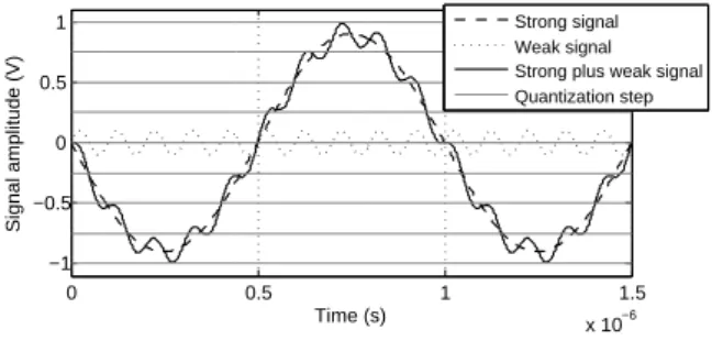
This issue is illustrated in Figure 1, where two signals (one strong and one weak, i.e. one with a high power level and one with a low power level) are represented as sine functions for convenience. When the signals are re-ceived together, the dynamic range of the total signal is driven by the strong signal’s dynamic range. Thus on the ADC’s full resolution, only a few bits are used to digitize
0 0.5 1 1.5 x 10⁻⁶ −1 −0.5 0 0.5 1 Time (s) Signal amplitude (V) Strong signal Weak signal Strong plus weak signal Quantization step
Figure 1. A strong and a weak signal being digitized together. When they are combined, the quantization noise level is higher than the weak signal level, leading to its degradation.
the weak signal. Moreover, the required ADC resolution to digitize the weak signal increases with the power ratio between the signals.
With a 100 dB power ratio and a 8 MHz bandwidth, it has been shown in [Vallerian et al., 2014] that an ADC of at least 21 bits is required and, to the best of the au-thors’ knowledge, such a resolution is not affordable with today’s ADC. Typically, ADCs providing high resolution are used in audio processing with a resolution of 24 bits for only 192 kHz of bandwidth. With an 8 MHz band-width, one cannot reasonably expect a higher resolution than 16 bits [Jonsson, 2010]. In this context, this paper presents an architecture aiming at relaxing the ADC con-straints by using two digitization branches.
This architecture is conceived based on the assumption that only one strong signal is present in the transmission band, whereas there can be several weak signals. Indeed a strong signal always comes from a sensor that is lo-cated near the gateway, generally in Line-of-Sight (LOS) propagation conditions, whereas a weak signal may come from various locations. Moreover, in urban sensor net-works, the nodes emit essentially short frames, so the in-terference probability is very low in the case of strong signals since only a small number of nodes is able to pro-vide such a strong signal [ETSI, 2011].
This paper is structured as follows: section 2 intro-duces the proposed architecture and in section 3, the im-plementation of this architecture on the Keysight’s ADS software is described. Then the simulation results, char-acterizing the architecture robustness on the hardware im-plementation impairments are given in section 4. Sec-tion 5 concludes this paper and gives direcSec-tions for future work.
2. Architecture description
2.1. Motivation and state of the art
It has been shown in [Vallerian et al., 2014] that the dy-namic range occupied by the various signals in our sce-nario of urban sensor networks is too high to properly digitize the whole band at once. Then, one solution to keep a full band digitization is to reduce this dynamic range, either by amplifying the small signals or by atten-uating the strong ones. To choose the best approach, one can consider that a strong signal always comes from a sensor that is located near the gateway in LOS propaga-tion condipropaga-tions, whereas a weak signal may come from a far wider area, as some sensors are located far from the gateway, underground or, more globally, in Non-Line-of-Sight (NLOS) propagation conditions. Then it is more likely to receive a weak signal than a strong signal.
As a consequence, it is assumed here that there will be one strong signal co-existing with several weak signals. Hence, it seems more relevant to attenuate the strong sig-nal than to amplify the weak sigsig-nals.
Figure 2 shows the required resolution when demodu-lating two signals with different power levels ([Vallerian et al., 2014]). Assuming as a target that a resolution of 16 bits is feasible, the dynamic range of the signals should be reduced to a maximum of 70 dB. If a margin of 2 bits is taken between the ADC’s resolution and its Effective Number Of Bits (ENOB), then the strong signal should be attenuated by 40 dB. The saving of resolution bits and the dynamic range reduction are highlighted in Figure 2 with dashed lines.
0 20 40 60 80 100 3 7 11 15 19 23 R e q u ir e d r e s o lu ti o n Filter attenuation S a v e d b it s 0 20 40 60 80 100 8 128 2048 32768 524288 8388608 R e q u ir e d n u m b e r o f q u a n ti z a ti o n s ta te s
theoretical required ADC resolution theoretical required number of quantization states
Figure 2. The required resolution to properly demodulate two signals with high dynamic range. 21 bits are required to digitize the signals with a dynamic range of 100 dB, but the required resolution can be reduced to 14 bits if the dynamic range is re-duced by 40 dB.
The problem addressed in this paper may seem to be similar to the one of interference cancellation ([Borre-mans et al., 2011; van den Heuvel and Cabric, 2010]). However, in these works, it is always assumed that the in-terference must be totally eliminated, whereas in our case it is also a signal of interest. In [Wang et al., 2005], an architecture is presented to improve the near-far perfor-mance in Code Division Multiple Access (CDMA). How-ever, it requires to know the signals signatures and thus it requires a minimum number of previously received sig-nals. Moreover, the performance is discussed by the au-thors for a power ratio of only 10 between the signals.
Another architecture, using a Minimum Mean-Square Error (MMSE) filter and taking advantage of both succes-sive interference cancellation (SIC) and parallel interfer-ence cancellation (PIC), was proposed in [Krzymien and Schlegel, 2011]. However, the considered maximum dy-namic range is of the order of tens of dB and is lower than the one in our scenario.
Another way to reduce the dynamic range can be to subtract the strong signal from the received signal, as proposed in [Nie et al., 1999]. This method can bring some instability to the system, as the subtracted signal is generated through a prediction algorithm. Indeed predic-tion algorithms are intended for slowly-varying signals [Fletcher et al., 2007], whereas in our case the dynamic range can be very high.
In this paper, the proposed solution is to use a notch filter that attenuates the strong signal and leaves the rest of the transmitted band unchanged. The main challenge with this approach is to attenuate the strong signal re-gardless of its frequency while preserving the rest of the band.
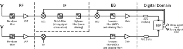
2.2. Receiver’s architecture description
The proposed architecture is depicted in Figure 3 and has a notch filter to attenuate the strong signal. Two solu-tions are possible to reconfigure this receiver’s architec-ture in order to properly attenuate the strong signal: ei-ther the notch filter’s central frequency can be modified to match the strong signal’s central frequency, or the strong signal’s carrier frequency can be translated to match the notch filter’s central frequency.
With the first solution, a reconfigurable filter should be used and its stop-band should be 8 MHz wide. With the second solution, the strong signal should be translated into an intermediate frequency that is equal to the notch filter’s central frequency and translated in baseband after-ward. In both cases, the strong signal’s central frequency must be evaluated before the reconfiguration.
Notch filter (strong signal attenuation)
Gain
Gain
LNA (16 bits)ADC
ADC 5 bits DSP Bandpass filter Bandpass filter Lowpass filter (ADC’s anti-aliasing filter) LO LO2 LO1 Highpass filter (noise aliasing) LNA RF IF BB Lowpass filter (ADC’s anti-aliasing filter) Digital Domain Weak signal data Strong signal data
Figure 3. Schematic of the proposed architecture. The Coarse Digitization Path (on bottom) allows to digitize the strongest signal. Its frequency is digitally found, and then the signals are down converted on the Fine Digi-tization Path (on top) in order to attenuate the strongest signal by means of a notch filter, reducing the dynamic range of the signals.
The second solution (with a fixed filter) seems simpler to implement, as it only requires two mixers to perform the frequency translations. With the first method, a re-configurable filter with a high enough selectivity to at-tenuate the strong signal without affecting the rest of the band is required. The filter’s non-reconfigurability is thus an asset in terms of the architecture complexity. For this reason, in the sequel, the second solution was selected to attenuate the strong signal.
The strong signal’s carrier frequency is matched to the notch filter’s central frequency by using a frequency translation. Then, the strong signal’s central frequency must be computed by the digital part of the architecture (DSP) in order to set the frequency of the first local oscil-lator (LO1). To do so, the entire 8 MHz signal bandwidth must be digitized without passing through the notch fil-ter. The frequency seeking may be done by the means of a Fast Fourier Transform (FFT) in a second branch of the architecture. On this second branch, only the strongest signal will be digitized and the ADC resolution on this branch should be set in a such a way to be able to properly digitize only one signal. In [Vallerian et al., 2014], it has been shown that a resolution of 5 bits is sufficient to per-form this digitization.Therefore, in the following, the two branches of the proposed architecture are respectively re-ferred to as fine digitization path (FDP) and coarse digi-tization path(CDP).
In the architecture presented in Figure 3, the top and bottom branches represent the FDP and the CDP, respec-tively. In the CDP, the input signals are digitized after the frequency down conversion. Then, a Digital Signal Processor (DSP) performs the FFT and finds the strong signal’s carrier frequency by seeking the maximum fre-quency components of the spectrum. Then, it drives the Local Oscillators (LOs) of the FDP in order to synthesize this frequency.
On the FDP, the input signals are first down-converted
around an intermediate frequency through the LO1 to
make the strong signal frequency match the notch fil-ter’s central frequency. The signals are down converted
in baseband afterward by using the LO2 and then
digi-tized. The demodulation of the two baseband signals is performed by the DSP.
The noteworthy frequencies of this approach are rep-resented in Figure 4. fRF is the starting frequency of the
RF 8 MHz band. fSs and fSw are the strong and weak
signal baseband frequencies, and fSs,RFand fSw,RF are
the corresponding RF frequencies. fLO1 and fLO2 are
the LO1 and LO2 frequencies and fcCB is the notch
filter central frequency. fI is the starting frequency of the intermediate 8 MHz band. In the presented scenario, fI = fLO2. fcCB fOL1 fRF fI =fOL2 fSs,RFFrequency First translation Second translation fSw,RF fSs fSw
Figure 4. The noteworthy frequencies of the architecture, de-noting the frequencies of the signals and the starting frequency of the band in RF, IF and BB.
To perform the frequency conversion on the FDP, fLO1 should be set to make fSs,RF to be equal to fcCB:
fLO1= fSs,RF− fcCB (1)
The second frequency down conversion is intended to complete the baseband conversion initiated by LO1:
fLO2= fRF− fLO1 (2)
3. Simulation results
The proposed architecture has been implemented on the Keysight’s ADS software in order to study its perfor-mance. A strong and a weak signal are generated with a Binary Phase-Shift Keying (BPSK) modulation. Their power ratio is adjustable and an Additive White Gaus-sian Noise (AWGN) is introduced to simulate a tunable Eb/N0that is considered with respect to the weak signal.
As a reminder, in the case of AWGN noise, the theo-retical Bit-Error Rate (BER) for a BPSK modulation is:
BER = 1 2erfc r Eb N0 ! (3)
where erfc(x) is the complementary Gauss error function of x.
The architecture’s performance is measured as the dif-ference between the theoretical BER and the simulated BER. The BER is simulated through the Monte-Carlo method and is given in the following with a relative vari-ance of 0.01.
It is assumed that the strong signal’s spectrum is not spread, even if spreading is a common technique em-ployed in urban sensor networks. Indeed this technique is used to improve the sensitivity of a technology, and is thus employed by communication protocols covering sensitive applications (whose sensors are located indoor or underground for example). As we consider that the strong signal is emitted in LOS conditions, it is assumed the employed communication protocol (covering low data rate applications) will not use such a technique. Its band-width is considered to be 50 kHz, which is a common value for this kind of signals (ETSI [2011]). If its band-width is higher, it is assumed that its power will be lower. Then a partial attenuation would still be efficient, as the strong signal should be less attenuated to reach a sustain-able dynamic range. The weak signal is assumed to have a bandwidth of 200 kHz.
Despite the assumptions made (the strong signal is emitted with a small bandwidth, and only one strong sig-nal is present on the band), the studied case is a worst-case scenario: the presence of two signals with a 100 dB power ratio, which is rare in practice.
Filter 3 (notch) Variable gain ADC Filter 1 (bandpass) Filter 4 (lowpass) LO2 LO1 Filter 2 (bandpass) Demodulation Simulation parameters Strong signal + Weak signal + Noise
Figure 5. FDP implementation on the ADS software. The input signals are translated on the notch filter to attenuate the strongest one, and then translated in baseband to be digitized. The frequencies of LO1 and LO2 are set from the simulation parameters.
The FDP implementation is presented in Figure 5. For the sake of readability, the signals generation and demod-ulation are not shown in this figure. The input signals (in-cluding the strong and the weak signals and the noise) are
first filtered to avoid aliasing during the LO1 frequency translation. The second filter in the chain eliminates the signals’ image frequency, and the filter 3 is the notch fil-ter that attenuates the strong signal. Affil-ter LO2’s base-band translation, the signals then pass through the filter 4, which is the ADC’s anti-aliasing filter. They are even-tually digitized and demodulated by the DSP. The notch filter’s central frequency fcCB should be low in order to minimize the quality factor of the filter (and thus to guar-antee a simpler implementation).
Because of the 8 MHz bandwidth of the considered communication system, the intermediate band should be-gin at frequencies higher than 4 MHz to avoid aliasing during the baseband translation. fcCBis then chosen to be 12 MHz to be able to cut the strong signal regardless of its frequency. It is imposed that the filter should not at-tenuate other signals than the strong signal and its two ad-jacent channels. The strong signal channel being 50 kHz, the cut bandwidth should be 150 kHz. This leads to a quality factor of 80, which is a reasonable value consid-ering today’s technology. In a first step, the signals should be sufficiently far from each other to avoid any influence from the notch filter on the weak signal. The signals’
baseband frequencies are then set to be fSw = 2 MHz
and fSs= 5 MHz, respectively.
As mentioned, the architecture implementation is vali-dated through the simulated BER. The BER is plotted as a function of Eb/N0 in the Figure 6. The thin solid line represents the theoretical BER, calculated for a BPSK modulation based on equation (3). The thick solid line is the simulated BER with the proposed architecture and the dashed line is the BER with a classical architecture (i.e. the same architecture without the notch filter and the intermediate band translation).
0 1 2 3 4 5 6 7 8 10−4 10−3 10−2 10−1 100 E b/N0 (dB) BER
Simulated BER with the notch filter Simulated BER without the notch filter Theoretical BER (BPSK modulation)
Figure 6. Simulated BER of the weak signal with the proposed implementation and with a more classical implementation. In simulations, the BER is lightly degraded with respect to the the-oretical one, but they are still of same order.
The BER with the classical architecture is a reference to which the BER with the proposed architecture is com-pared to. It can be seen that with a classical architecture, Eb/N0is degraded by about 0.5 dB. This is due to the fil-ters that lightly corrupt the signal but sufficiently to rise Eb/N0. It can be noted that this degradation does not depend on Eb/N0.
With the proposed architecture, Eb/N0is degraded by only 0.3 dB with respect to the classical architecture, be-cause of the intermediate band frequency translation’s fil-ters. This implementation can then be used for further studies, as it provides a very small degradation with re-gards to a classical architecture.
The CDP is simpler to implement since no additional frequency translation is required, only one frequency translation is performed to translate the transmission band into baseband. The strong signal frequency measurement must be performed on this branch. To do so, an FFT is done and the maximum frequency component is found.
4. Robustness of the proposed architecture
Compared to the implementation presented in the pre-vious section, the notch filter is changed to a cut-band filter, replacing the two bandpass filters. This implemen-tation increases the simulation time but is more realistic.4.1. Overall simulation parameters
To test the robustness of the proposed architecture, sev-eral parameters are to be considered. The notch filter should attenuate the strong signal without affecting the other ones. It was established in section 3 that the filter should have a 50 kHz cut band and should not affect other signals in a band wider than 150 kHz. The filter order and cut bandwidth (i.e. the filter selectivity) play an important role on the architecture performance, hence several sim-ulations are performed in order to establish their required characteristics which are not affecting the weaker signals. Another important parameter is the oscillators accu-racy. Indeed, since the oscillators’ frequencies are set from the strong signal’s frequency measurement through (1) and (2), a measurement error implies that the strong signal will not be translated exactly on the notch filter’s central frequency and it will be only partially attenuated. In order to study the influence of these frequencies generation accuracy on the overall architecture perfor-mance, several simulations were performed. First, the notch filter’s selectivity and the signal’s frequency prox-imity have been varied and second, the LOs frequency ac-curacy limits have been tested. Then, the oscillators
fre-quencies are set directly from the simulation parameters giving the central frequencies of each channel. This al-lows to isolate the different parameters and to study each of them separately, as the strong signal frequency mea-surement is not susceptible to be a source of error.
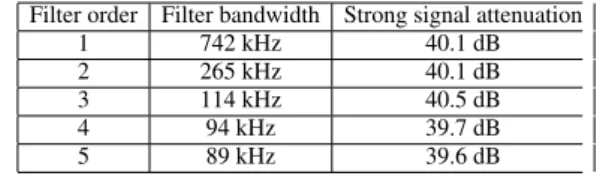
4.2. Influence of the notch filter selectivity
It has been shown in section 2 that the notch filter must provide a 40 dB attenuation. To reach this attenuation, the filter is tested with several orders and its bandwidth must be adapted depending on this order. The purpose of a first set of simulations is thus to give the filter bandwidth that provides a 40 dB attenuation for several orders. The fil-ter order is chosen to vary from 1 to 5, this range being a good compromise between complexity and efficiency. The simulated bandwidths are presented in Table 1 and these values are used in the following in the filter selec-tivity simulations.
Table 1. Notch filter attenuation on a strong signal of a 50 kHz band-width, depending on the filter’s order and bandwidth
Filter order Filter bandwidth Strong signal attenuation
1 742 kHz 40.1 dB
2 265 kHz 40.1 dB
3 114 kHz 40.5 dB
4 94 kHz 39.7 dB
5 89 kHz 39.6 dB
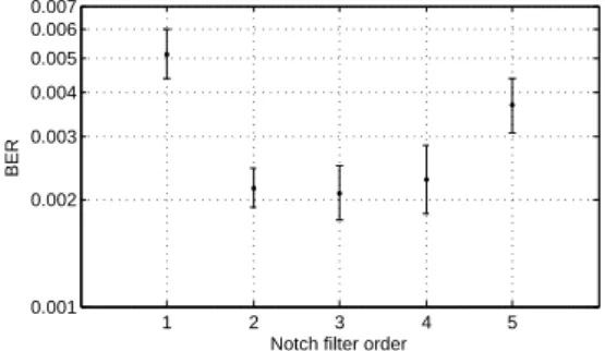
It is considered that the frequency spacing between the signals and oscillators frequencies are fixed and the effect of the filter selectivity on the weak signal’s BER is studied here. One channel spacing (i.e. 50 kHz) is kept between the strong and weak signals. In baseband, the strong signal begins at 1.975 MHz and ranges to 2.025 MHz and the band that can be affected by the filter thus ranges from 1.925 MHz to 2.075 MHz. As for the weak signal’s baseband channel, it is set to range from 1.725 MHz to 1.925 MHz to avoid being attenuated by the filter. In the performed simulations, Eb/N0is 7 dB with respect to the weak signal. The Ss/Swratio is set to 80 dB instead of 100 dB because of the use of transient simulation which is less efficient when simulating high dynamic range signal but without any loss in the signifi-cance of these simulations.
The ADC resolution is set to 30 bits on the reference path to be high enough not to disrupt the BER measure-ment. A BER test is performed on the weak signal for every filter order. A filter order is thus validated if the simulated BER is equivalent to the theoretical one (which is of the order of 2 · 10−3, from Figure 6).
1 2 3 4 5 0.001 0.002 0.003 0.004 0.005 0.006 0.007
Notch filter order
BER
Figure 7. Simulated BER regarding the notch filter selectivity when the signals are close in frequency. The BER is degraded for the order 1 by the filter attenuation on the weak signal, and for the order 5 by the filter phase shift that affects the weak sig-nal.
Table 2.Simulated BER regarding the notch filter selectivity
Filter order BER
1 5.11 · 10−3
2 2.15 · 10−3
3 2.08 · 10−3
4 2.27 · 10−3
5 3.67 · 10−3
The simulation results are presented in Table 2 and are plotted in Figure 7. In these simulations, the BER is
com-0 2 4 6 8 10 12 14 16 18 20 22 24 26 10 15 20 25 30 35 40 45 Frequency shift ∆fSs (kHz)
Strong signal attenuation (dB)
Figure 8. Strong signal attenuation regarding the measured fre-quency error. As the filter should have a minimum attenuation of 30 dB, a measured frequency error less than 10 kHz is re-quired.
−5 0 5 10 15 20 25 30 35 40
10−3 10−2
Measured frequency error ∆fSs(kHz)
BER
Figure 9. Simulated BER regarding the measured frequency er-ror. The BER is degraded when the measured frequency error is higher than 15 kHz.
puted with a 95 % confidence interval. When the filter order is 1, the BER is degraded because of the filter at-tenuation. For orders from 2 to 4, the BER is equivalent to the theoretical one and is of the order of 2 · 10−3. With an order 5, the filter phase shift becomes too important and affects the weak signal integrity, and leads to an im-portant BER degradation.
It is considered in the following that the order 3 is the best compromise between the non-attenuation of the weak signal and its phase shift.
4.3. Influence of the local oscillator’s frequencies accuracy
In the final receiver architecture, the oscillators’ fre-quencies are set from a measurement of the strong sig-nal’s carrier frequency. Thus they are susceptible to be inaccurate because of a measurement error. To simulate the effect of the oscillators’ frequencies accuracy, an error ∆fSsis introduced on fSsin the calculation of fOL1and fOL2(defined by equations (1) and (2)), which are still set from the simulation parameters (and not from a measure-ment on the signals). So the strong signal is translated on the filter’s central frequency with a small frequency shift ∆fSs. This shift is canceled during the baseband conver-sion, so it does not affect the weak signal demodulation.
The filter order is set to 3 and the signals frequencies are set to 1 MHz for the weak signal and 2 MHz for the strong signal, so the filter selectivity cannot affect the weak signal. In the intermediate band, the strong signal is now translated on the frequency fcCB− ∆fSs. Then, the filter is less efficient to attenuate the strong signal. A series of BER simulations are performed to find the os-cillator’s frequencies accuracy requirement to sufficiently attenuate the strong signal and to properly demodulate the weak signal. A simulated BER close to the theoretical one means that the filter properly attenuates the signal.
The architecture should be capable of digitizing an in-put 80 dB power ratio with 12 bits, since the targeted resolution improvement is 7 bits. In Figure 2, one can see that such a resolution corresponds to a power ratio of about 50 dB. Thus the filter attenuation should be at least 30 dB.
A series of simulations intends to evaluate the strong signal attenuation depending on the frequency shift and the results are represented in Figure 8. As can be seen, to guarantee a higher attenuation than 30 dB (i.e. a re-jection of the strong signal of more than 30 dB), the fre-quency measurement error should be less than 10 kHz.
The shift between the attenuation at ∆fSs= 0 kHz and
the BER measurement tolerance range. Then the BER should be simulated for this error range. The simulated BER is plotted in Figure 9, where the BER is represented as a function of the error on the fSsmeasurement. Due to the confidence interval, the error domain in which the weak signal is properly demodulated cannot be precisely bounded; however it can be estimated to be between 0
and 15 kHz. Thus, the measurement error on fSsshould
be kept in this interval.
5. Conclusion
In this paper, a dual branch receiver architecture ca-pable of processing high dynamic range signals and thus relaxing the digitizer constraints is proposed. The pro-posed architecture assesses a problem commonly encoun-tered in urban sensor networks in particular and in the IoT communications in general, which is the simultaneous re-ception of signals with very different power levels.
The architecture has been implemented on Keysight’s ADS software to evaluate its feasibility. The simulations results show that the notch filter implementation is not constraining, since a filter of order 3 is enough to properly attenuate the strong signal without affecting the neighbor channels.
Moreover, the robustness related to the strong signal carrier frequency drift has been simulated. The results are quite satisfying, since a precision of 15 kHz on a 50 kHz channel is required. This means that some drift can be accepted on the frequency measurement.
The proposed architecture is then an efficient way to reduce the ADC requirements when digitizing multiple signals in urban sensor networks. Globally, instead of us-ing a 21 bits ADC, the proposed architecture uses two branches, one with a 5 bit ADC, for the strongest signal and one with a 14 bit ADC for all other signals. When taking into account the RF architecture impairments, the required ADC’s resolution on the fine digitization path increases from 14 to 16 bit. Future work will focus on testing its performance in a more realistic case, by using real signals emitted by SRDs.
A further study will be done on the best way to per-form the frequency measurement of the strong signal. In this paper it has been assumed that an FFT was used but it could also be done using a filter bank for a faster mea-surement.
Another work to be done on this architecture is to study its sensitivity and non-linearity requirements, as they are
very important regarding the high dynamic range the ar-chitecture is intended to receive.
Acknowledgment
This work has been funded by an Orange Labs research grant and the authors wish to thank Orange Labs research team for fruitful discussion and for their collaboration in this project. The authors declare that they have no com-peting interests. Further additional data cannot be made publicly available.
References
Borremans, J., G. Mandal, V. Giannini, B. Debaillie, M. Ingels, T. Sano, B. Verbruggen, and J. Craninckx (2011), A 40 nm CMOS 0.4-6 GHz Receiver Resilient to Out-of-Band Block-ers, J. Solid-State Circuits, 46(7), 1659–1671.
Dardaillon, M., K. Marquet, T. Risset, J. Martin, and H.-P. Charles (2014), Cognitive radio programming survey, in Handbook of Research on Software-Defined and Cognitive Radio Technologies for Dynamic Spectrum Management, edited by N. Kaabouch and W.-C. Hu, IGI Global.
ETSI (2011), Electromagnetic compatibility and Radio spec-trum Matters (ERM); System Reference document (SRdoc): Spectrum Requirements for Short Range Device, Metropoli-tan Mesh Machine Networks (M3N) and Smart Metering (SM) applications, TR 103 055.
Fletcher, A., S. Rangan, V. Goyal, and K. Ramchandran (2007), Robust predictive quantization: Analysis and design via con-vex optimization, Selected Topics in Signal Processing, IEEE Journal of, 1(4), 618–632, doi:10.1109/JSTSP.2007.910622. Gantz, J., and D. Reinsel (2012), The digital universe in 2020: Big data,bigger digital shadows, and biggest growth in the far east, IDC iView : IDC Anal. Future, 2007, 1–16. Jonsson, B. (2010), A survey of A/D-Converter performance
evolution, in Electronics, Circuits, and Systems (ICECS), 2010 17th IEEE International Conference on, pp. 766–769, doi:10.1109/ICECS.2010.5724625.
Krzymien, L., and C. Schlegel (2011), Near-Far Resistant MIMO Iterative Receiver for Uplink LTE, in Communica-tions (ICC), 2011 IEEE International Conference on, pp. 1– 5, doi:10.1109/icc.2011.5963041.
Nie, H., A. Salkintzis, and P. Mathiopoulos (1999), A new ap-proach for mitigating A/D conversion requirements in soft-ware radio base stations, in Vehicular Technology Confer-ence, 1999. VTC 1999 - Fall. IEEE VTS 50th, vol. 5, pp. 2810–2814 vol.5, doi:10.1109/VETECF.1999.800299. Vallerian, M., G. Villemaud, B. Miscopein, T. Risset, and
F. Hutu (2014), SDR for SRD: ADC specifications for re-configurable gateways in urban sensor networks, in Radio and Wireless Symposium (RWS), 2014 IEEE, pp. 178–180, doi:10.1109/RWS.2014.6830084.
van den Heuvel, J., and D. Cabric (2010), Spatial filter-ing approach for dynamic range reduction in cognitive ra-dios, in Personal Indoor and Mobile Radio Communications (PIMRC), 2010 IEEE 21st International Symposium on, pp. 2657 –2662, doi:10.1109/PIMRC.2010.5671790.
Wang, S., S. Kim, L.-H. Sun, H. Kim, S. Lee, S. R. Sub-ramanya, K. Kim, and B. Yi (2005), Blind adaptive mul-tiuser detection, in Global Telecommunications Conference, 2005. GLOBECOM ’05. IEEE, vol. 6, pp. 5 pp.–3737, doi: 10.1109/GLOCOM.2005.1578468.
Corresponding author: Florin Hut¸u, CITI laboratoy, 6 av.
des Arts, 69621, Villeurbanne, France; [email protected]
![Figure 2 shows the required resolution when demodu- demodu-lating two signals with different power levels ([Vallerian et al., 2014])](https://thumb-eu.123doks.com/thumbv2/123doknet/12873439.369442/3.892.173.461.730.926/figure-required-resolution-demodu-demodu-signals-different-vallerian.webp)