HAL Id: tel-01698831
https://tel.archives-ouvertes.fr/tel-01698831v3
Submitted on 16 Mar 2018
HAL is a multi-disciplinary open access archive for the deposit and dissemination of sci-entific research documents, whether they are pub-lished or not. The documents may come from teaching and research institutions in France or abroad, or from public or private research centers.
L’archive ouverte pluridisciplinaire HAL, est destinée au dépôt et à la diffusion de documents scientifiques de niveau recherche, publiés ou non, émanant des établissements d’enseignement et de recherche français ou étrangers, des laboratoires publics ou privés.
alloys for high electron mobility transistors by
transmission electron microscopy
Hichem Ben Ammar
To cite this version:
Hichem Ben Ammar. Investigation of ternary AlIn and quaternary AlGaIn alloys for high electron mobility transistors by transmission electron microscopy. Physics [physics]. Normandie Université, 2017. English. �NNT : 2017NORMC241�. �tel-01698831v3�
Investigation of ternary AlInN and quaternary AlGaInN alloys for High
Electron Mobility Transistors by Transmission Electron Microscopy
THESE
THESE
Pour obtenir le diplôme de doctorat
Spécialité PHYSIQUE
Préparée au sein de l’ENSICAEN et de l’UNICAEN
Présentée et soutenue par
Hichem BEN AMMAR
Thèse soutenue publiquement le 01/12/2017 devant le jury composé de
Madame Valérie POTIN Maître de conférences HDR,
Université de Bourgogne Franche-Comté Rapporteur Monsieur Jean-Luc MAURICE Directeur de Recherche CNRS,
École Polytechnique Palaiseau Rapporteur Madame Laurence MECHIN Directeur de Recherche CNRS,
ENSICAEN Examinateur
Monsieur Farid MEDJDOUB Chargé de Recherches CNRS HDR,
Université de Lille 1 Examinateur
Madame Magali MORALES Maître de conférences HDR,
UNICAEN Examinateur
Monsieur Pierre RUTERANA Directeur de Recherche CNRS,
ENSICAEN Directeur de thèse
i
Acknowledgments
This thesis has been carried out at CIMAP Laboratory (Centre de recherche sur les Ions, les Matériaux et la Photonique) from October 2014 to October 2017. It was carried out in the scope of the ANR-LHOM project. I’m thankful to Pierre RUTERANA my research supervisor for the countless fruitful discussions, suggestions and support of my work.
My grateful thanks go to Valérie Potin and Jean Luc Maurice who have kindly accepted to review my manuscript and be part of the jury. Farid MEDJDOUB of IEMN carried for device fabrication/characterization and has kindly accepted to be member of the jury, I am very thankful to his valuable inputs. Special thanks go to Magali MORALES, the coordinator of the LHOM project and for having accepted to judge my work as a member of the jury. I am grateful to Laurence MECHIN of GREYC for having shared her valuable expertise AFM, and for accepting to judge my work as a member of my jury.
My gratitude goes to Albert MINJ for his help and the answers he brought to my many questions. I am also grateful toward all the collaborators from the different institutions involved in the LHOM project, especially Piero GAMARRA and his colleagues from III-V Labs who performed the growth of most of the materials that have been investigated. I also would like to acknowledge Lorenzo RIGUTTI for the APT measurements.
I would like to thank all the following people that were involved not only in my work but also in everyday life in the lab, special thanks to Marie-Pierre CHAUVAT, Delphine and Phillippe MARIE, Michael BOISSERIE, Thomas DIETSCH, Emmanuel GARDES, Cedric FRILAY, Sylvain FOUBERT, Patrick VOIVENEL, Cédric GENDREAU, and all the colleagues not mentioned from the different teams and laboratories of CIMAP and GREYC.
I would like to thank finally all my friends, Florian, Jennifer, Nicolas, Lucile, Nicolas (they are two), Charlène, Anaïs, Clément, Basile, … Thanks for all the enjoyable moments that we have spent together during these three years.
iii
The problem is not the problem; the problem is your attitude about the problem. “Cpt. Sparrow”
v
Table of contents
ACKNOWLEDGMENTS ... I TABLE OF CONTENTS ... V RÉSUMÉ ... 1 INTRODUCTION ... 9 1 PROPERTIES OF III-NITRIDES ... 17 1.1. Crystalline structure ... 171.2. Unit cell deformation: strain and stress ... 18
1.3. Spontaneous and piezoelectric polarizations ... 20
1.4. Properties of AlInN and AlGaInN alloys... 23
1.5. Structural defects in III-Nitrides ... 25
1.5.1. Point defects ... 26
1.5.2. Dislocations ... 26
1.5.3. Planar defects ... 28
2 CHARACTERIZATION TECHNIQUES ... 31
2.1. Atomic force microscopy ... 31
2.2. Electron microscopy ... 32
2.2.1. Scanning electron microscopy... 32
2.2.2. Transmission electron microscopy ... 33
2.2.3. Electron sources and electron guns ... 34
3 GROWTH CHAMBER HISTORY AND GEOMETRY: INFLUENCE ON AlInN AND AlGaInN ... 49
3.1. Metal-organic vapor phase epitaxy (MOVPE) ... 49
3.2. Samples presentation ... 51
3.2.1. Investigating the Origin of gallium ... 52
3.2.2. Gallium content and growth conditions ... 56
3.3. Conclusions ... 59
4 MOVPE OF AlInN AND AlGaInN: EFFECTS OF TDS AND IDS ... 61
4.1. Substrates ... 61
4.1.1. Al2O3 ... 62
4.1.2. Si ... 63
4.1.3. SiC... 63
4.1.4. GaN ... 64
4.2. Extrinsic degradations of AlGaInN and AlInN ... 64
4.2.1. Samples ... 65
4.2.2. Effects of sapphire and silicon substrate on the quality of GaN... 66
4.2.3. Sub-grain boundaries ... 67
4.2.4. Individual TDs and pinholes ... 70
4.2.5. The IDBs and interaction with a thin AlN interlayer ... 75
4.3. Summary ... 80
5 GROWTH PARAMETERS AND QUALITY OF BARRIER LAYERS ... 83
5.1. Introduction ... 83
5.2. Results and discussion ... 83
5.2.1. The Samples ... 83
5.2.2. Temperature and V/III ratio ... 84
5.2.3. Pressure ... 89
vi
6 INHERENT DEFECTS IN AlInN & AlGaInN ... 95
6.1. Introduction ... 95
6.2. Results and discussion ... 95
6.2.1. Samples ... 95
6.2.2. Effect of the layer thickness ... 96
6.2.3. Origins of the inherent degradations ... 106
6.3. Summary ... 112
7 CHARACTERIZATIONS OF HEMTS ... 113
7.1. Introduction ... 113
7.2. Results and discussion ... 114
7.2.1. Contacts optimization ... 115
7.2.2. AlN optimization ... 120
7.2.3. SiN passivation layer ... 121
7.3. Summary ... 124
CONCLUSIONS... 127
REFERENCES ... 131
1
Résumé
Les Nitrures
Les semi-conducteurs III-N possèdent des propriétés remarquables et sont largement étudiés depuis les années 90. D’une part, AlN, GaN et InN ont leurs bandes interdites directes à 6.2 eV, 3.39 eV et 0.65 eV, respectivement. Par conséquent, les alliages AlGaN, InGaN et AlInN couvrent le spectre de longueur d’onde du lointain ultra-violet (UV) au proche infrarouge (IR). En comparaison à d'autres semi-conducteurs III-V, III-As et III-P ne couvrent le spectre que de l’IR au jaune. D’autre part, les propriétés physiques et chimiques des III-N leur confèrent une bonne stabilité. Par conséquent les dispositifs à base de ces matériaux sont susceptibles de fonctionner dans des conditions extrêmes telles que très hautes températures ou forts courants. Les nitrures sont donc de très bons candidats pour la fabrication de composants avec applications tant dans les domaines civils que militaires. Ils sont employés dans les diodes électroluminescentes (LED pour « light emitting diodes »), dans l’électronique de puissance, etc…. En effet les LEDs et les lasers bleus sont désormais disponibles sur le marché. Néanmoins, un certain nombre de problèmes subsistent. Les III-N sont le plus souvent utilisés sous forme de couches minces obtenues par la croissance épitaxiale sur des substrats faits d’autres matériaux. Ceci est à l’origine de la contrainte entre couche et substrat et de grandes densités de défauts cristallins qui dégradent la qualité des dispositifs et réduit leur efficacité. Plus particulièrement, il reste quelques défis technologiques dont 1) la fabrication de sources de lumière blanche sans avoir recours à l’utilisation d’un phosphore convertisseur. 2) la fabrication de transistors à effet de champ, appelés aussi Transistors à Haute mobilité Electronique (HEMT pour « high electron mobility transistor ») à base de barrière AlInN épitaxié sur GaN, pouvant travailler avec de forte densité de puissance à très haute fréquence.
Le premier rapport connu sur AlN synthétisé en chauffant de l’azote gazeux avec de l’aluminium dans un tube a été publié en 1907. Plus tard en 1910, InN a été obtenu et, enfin, en 1932 le GaN a été produit par un mélange de gaz d'ammoniac condensé et de « gallium tribromide ».
2
Quand des techniques de croissance plus modernes ont été développées, GaN a ensuite été épitaxié en phase vapeur hybride (HVPE pour « hydride vapor phase epitaxy ») en 1969. Par la suite, AlN et GaN ont été synthétisés sur saphir par l’épitaxie en phase vapeur d’organométallique (MOVPE pour « metal organic vapour phase epitaxy »), mais aussi par épitaxie par jets moléculaire (MBE pour « molecular beam epitaxy »). Au début des années 1980, les recherches sur ces composés ont explosé à partir de la mise au point des couches tampons déposées à basse température et du dopage p-GaN par le magnésium, conduisant naturellement à la fabrication de LEDs comme UV-LEDs, des Lasers et LEDs violettes.
Parallèlement au développement du marché des LEDs, les dispositifs microélectroniques et plus particulièrement les HEMTs connaissent un essor important. En effet, en comparaison à d'autres semi-conducteurs comme le silicium on s'attend à de plus forte puissance en utilisant les nitrures. La première démonstration de la haute mobilité électronique a été faite sur l’héterostructure AlGaN/GaN grâce aux polarisations spontanée et piézoélectrique qui donnent naissance à une densité de gaz bidimensionnel (2DEG pour « 2 dimensional electron gas») à l’interface.
Parmi les alliages (Al, Ga, In)-N, Al1-xInxN a son paramètre accordé à celui du GaN pour x=0.18. En 2001, une étude théorique a montré que des HEMTs basé sur AlInN devraient présenter des performances meilleures que ceux utilisant des barrières AlGaN. Ceci grâce à la charge induite par une plus forte polarisation spontanée dans AlInN conduisant à une densité plus grande du 2DEG. Une autre propriété intéressante est la différence entre les indices de réfraction entre AlInN et GaN (environ 7%), ainsi des miroirs de Bragg (DBR pour « distributed Bragg reflectors ») avec une réflectivité presque de 100% ont été fabriqués. Ceci a constitué un pas important vers la fabrication de laser à cavité verticale (VCSEL pour « vertical-cavity surface-emitting laser »)
En comparaison à l’AlInN, l'alliage quaternaire AlGaInN offre des degrés de liberté supplémentaires. En effet par rapport au GaN, on peut 1) accorder séparément les bandes interdites et les paramètres de maille et 2) ajuster séparément les polarisations spontanée et piézoélectrique
3
Objectifs
Ce travail a été effectué dans le cadre du projet ANR-LHOM (AlInN Layers and AlInN Heterostructures for Optimized high electron Mobility transistors). En collaboration avec les équipes partenaires du projet (IEMN, III-VLab, GREYC), ma contribution a été centrée sur la caractérisation par microscopie électronique en transmission (TEM pour « transmission electron microscopie ») des alliages AlInN et AlGaInN. Le but était ainsi d'aider à comprendre les mécanismes de croissance de ces alliages et d’assurer le suivi de la structure des dispositifs vers une optimisation de leur performance.
La difficulté de l’épitaxie de ces matériaux réside dans le fait que les composés binaire de base ont des propriétés physiques assez différentes. Par exemple, les températures de croissance MOVPE pour AlN, GaN et InN sont >1200 °C, 1000 °C et < 600 °C, respectivement. Tous les travaux récents montrent que les surfaces de couches épitaxiales de ces alliages sont parsemées de pyramides inversées dénommées ‘pinhole’ dont la formation a été longtemps reliée à la présence des dislocations traversantes dans les couches sous-jacentes. Plus récemment, ce type de défauts a été aussi rapporté après une croissance d’AlInN sur du GaN avec taux de défauts très faible (<105 cm-2), il a alors été proposé qu’il devait y avoir un mécanisme intrinsèque de formation de ces pinholes par coalescence des zones de croissance à trois dimension (hillocks). Au cours de ce travail de thèse, on a donc cherché à comprendre la structure de ces alliages par une étude détaillée de microscopie. Ainsi, nous avons étudié le processus d’épitaxie MOVPE et les influences des paramètres de croissance sur la qualité des barrières. Ce faisant, nous avons mis en évidence les différents types de défauts à commencer par ceux provenant des couches sous-jacentes et leurs effets sur la structure de l’alliage. Ensuite, nous nous sommes attachés à analyser en détail les dégradations intrinsèques de ces alliages qui se manifestent spontanément lorsque l’épaisseur des couches est augmentée et sans présenter d’épaisseur critique de formation.
4
Ce travail est discuté en sept chapitres
Le chapitre 1 présente les propriétés structurelles des nitrures. Nous avons, d’abord, décrit la principale phase dans laquelle ces matériaux cristallisent (la structure wurtzite). Les propriétés de polarisations, les origines de la polarisation spontanée et piézoélectrique ont été ensuite discutées. Nous nous sommes ensuite intéressés aux alliages AlInN et AlGaInN pour lesquels nous avons récapitulées les principales propriétés structurelles. Finalement, les principaux défauts cristallographiques rencontrés dans la structure wurtzite ont été discutés.
Le chapitre 2 concerne les techniques de caractérisation utilisées durant ce travail. Les topographies ont été étudiées avec la microscopie à force atomique (AFM pour « atomic force microscopy ») pour déterminer les morphologies de surface et les rugosités. Une bonne partie des lames minces pour microscopie électronique en transmission (TEM pour « transmission electron microscopy ») a été préparée par faisceaux d’ions focalisés (FIB pour « focused ion beam »). Le TEM constitue la technique de caractérisation principale utilisée durant ce travail de thèse. Grâce au TEM, les défauts cristallins sont observés, différenciés et caractérisés par type et origine potentiel. La microstructure des couches minces a été observée jusqu’à l’échelle atomique.
Nous avons aussi pu avoir accès à la sonde atomique tomographique (APT pour « atome probe tomography ») qui a été utilisée pour déterminer la distribution atomique tridimensionnelle. Cette dernière a été le fruit d’une collaboration avec le GPM de l’université de Rouen. Elle nous a apporté une bonne confirmation des résultats de TEM.
Le chapitre 3 présente d’abord la technique de croissance MOVPE. Elle est à l’origine de toutes les couches minces étudiées ; elles ont été élaborées dans deux chambres de croissance de géométries différentes, l’une dite horizontale, la seconde verticale. La première chambre permet de croître des alliages AlInN ternaires, alors que dans le bâti vertical, une incorporation non intentionnelle de galium est observée conduisant à un alliage quaternaire AlGaInN. Dans ce chapitre, nous avons essayé d’expliquer l’origine de l’incorporation du Ga en analysant les effets de la géométrie de la chambre et l’influence des paramètres de dépôt.
5
Suite à cette étude, les sources de cette incorporation sont les parois internes de la chambre verticale ainsi que de la paroi d’accès des organométalliques connue sous le nom de « shower head ». Nous avons ensuite observé que la quantité de gallium incorporée peut être réduite de deux manières. 1) une réduction à 2% si la chambre de dépôt est préalablement nettoyée donc en éliminant le gallium résiduel, ou 2) à 6% en faisant l’épitaxie à 80 Torr qui semble diminuer la réactivité du gallium résiduel.
Le chapitre 4 a été consacré à l’étude des défauts extrinsèques qui sont dus aux dislocations traversantes et des domaines d'inversions issus du GaN. En croisant, les données d’AFM et du TEM, nous avons mis en évidence que les dislocations de type « a+c » et « c » s’ouvrent en pinholes localisés au milieu d’hillocks ayant des dimensions plus grandes qu’une dislocation de type « a ». Parmi les défauts observés, nous avons répertorié des tranchés, dus à des domaines d’inversion dans le GaN. La formation des tranchées a été expliquée par la dynamique de croissance autour d’une région GaN de polarité azote au-dessus duquel la vitesse de croissance est réduite. On montre aussi que la contrainte observée entre les régions de différentes polarités est accompagnée par 1) la fluctuation de compositions entre des régions riches en aluminium ou en indium et 2) l’interaction avec une couche AlN à l’interface AlGaInN/GaN. Le résultat sur la morphologie de surface se manifeste par l’apparition d’un certain nombre de tranchées autour du domaine d’inversion. En fonction de l’épaisseur de la couche mince, ces tranchées peuvent présenter de pinholes séparés ou non.
Par ailleurs, dans cette analyse, nous montrons qu'une certaine population des « pinholes » n'est pas reliée aux dislocations et découle donc d’une dégradation intrinsèque de la couche d’alliage.
Dans chapitre 5, nous montrons d’abord que la condition d’accord de paramètres de mailles peut être obtenue pour des températures de croissance différentes. Cependant, la qualité des couches dépend fortement de ces conditions de croissance et notamment, la rugosité de surface peut être réduite avec un jeu de paramètres adéquats. Dans les conditions que nous avons pu explorer, la morphologie obtenue indique que la croissance est toujours de façon tridimensionnelle.
6
Le chapitre 6 présente une analyse des défauts intrinsèques de ces alliages. En effet, même avec des conditions de croissance optimisées et pour des couches accordées en paramètres de maille, si on augmente l'épaisseur on observe 1) de fortes fluctuations de compositions pouvant dépasser les 30% 2) des structures polycristallines ayant des désorientations localisées 3) une forte rugosité indiquant une accentuation du mode de croissance en 3D.
Durant ce travail, nous avons collaboré aussi à la caractérisation de dispositifs HEMTs. Les résultats de cette contribution sont récapitulés dans le chapitre 7. Les principaux constituants optimisés sont les contacts ohmiques et Schottky ainsi que la couche de passivation. Une comparaison des caractéristiques de nos dispositifs avec la littérature y est rapportée. Grâce aux améliorations apportées durant le projet LHOM aux différentes parties du dispositif, nous avons atteint une mobilité électronique de l’ordre de 1800 cm2V-1s-1 avec une densité du 2DEG de 2×1013 cm-2. Actuellement, ces transistors peuvent supporter des tensions jusqu’à 200 V et ont démontré une fréquence de coupure de 260 GHz.
9
Introduction
I. III-Nitrides
Group III-Nitrides based on aluminum, gallium and indium exhibit outstanding properties and have been investigated since early 1900. On one hand, AlN, GaN, and InN have direct band gaps of 6.2 eV, 3.39 and 0.65 eV, respectively[1]. Therefore, their alloys cover from deep ultraviolet (UV) to near infrared (IR) across the visible range of wavelengths. In comparison, other III-V semiconductors such as III-As and III-P have their band gap ranging from IR to yellow as shown in figure 1.
Figure 1: Band gap of semiconductors plotted as a function of their lattice parameter[2].
On the other hand, the short bond lengths of the binary compounds lead to high bond energy. Therefore, III-Nitrides have high thermal and chemical stability. Thus they can stand harsh working conditions such as high temperatures as well as high voltages and currents. These properties make them suitable for many applications in both civil and military fields; high power electronics, LEDs, etc.…. Indeed, the blue LEDs and lasers are now commercially available, as well as their translation to solid-state lighting. The main drawback of III-N is that no suitable native substrate is available for the growth of the active devices; this is at the origin of high strain and high density of crystallographic defects in the heterostructures which degrade the quality of the devices. In particular, there are still two main challenges: 1) the fabrication of white light without the use of phosphors which will rely on the growth of good quality high indium content InGaN/GaN quantum wells, 2) the production of high-performance AlInN/GaN high mobility transistors for high speed, high density, high power telecommunication.
10
The first record for AlN was in 1907[3] which was synthesized by heating gaseous nitrogen with aluminum in a tube. Later, in 1910[4], InN was synthesized and then in 1932[5] GaN was produced by a mixture of condensed ammonia gas and gallium tribromide. After modern growth techniques have been developed, GaN was epitaxially grown by hybrid vapor phase epitaxy (HVPE) in 1969[6] and then AlN and GaN by metal organic vapor phase epitaxy (MOVPE)[7] and later AlN by means of molecular beam epitaxy (MBE)[8]. In these instances, the used substrate was sapphire. Starting in the 1980’s, these compounds went under huge investigation after the discovery of GaN p-doping by magnesium[9,10] which bridged towards the fabrication of light emitting diodes (LEDs) such as UVLEDs[11,12], lasers[13], and violet LEDs[14].
Beside the development of the LED market, microelectronic devices, especially high electron mobility transistors (HEMTs), have also been extensively investigated. Indeed, in comparison to other semiconductors like silicon-based devices, it is expected to attain higher output power densities using III-N devices. The first demonstration of enhanced electron mobility has been demonstrated on AlGaN grown on GaN[15,16] which is due to strain and the spontaneous piezoelectric polarization which can be tuned to have a two-dimensional gas (2DEG) at an adequate hetero-interface.
Among the (Al, Ga, In)-N alloys family, InxAl1-xN exhibits the above properties and in addition, it can be grown lattice-matched (LM) to GaN and thus suppress the strain when the molar fraction of InN is x≈18%. In 2001, Kuzmik et al.[17] theoretically predicted that LM-AlInN based HEMT should exhibit higher drain currents than those using AlGaN barriers. He pointed out that this is due to the higher polarization-induced charge in AlInN leading to a higher density of 2DEG. Another interesting property of these LM alloys was reported just after in 2003 by Carlin and Ilegems[18,19], they grew LM-AlInN/GaN distributed Bragg reflectors with a nearly 100% reflectivity due to the high contrast between the refractive indices around 7%. This constituted an important step toward vertical cavity surface emitting lasers (VCSELs). Since then, as shown in figure 2 which represents a statistical survey retrieved from Web of Science[20], the number of publications counts using (In, Al)N as keywords have increased steadily. However, since 2010, the number has settled to
11
a maximum of around 100/year. This is probably due to the difficulties encountered in growing high-quality layers[18,19,21].
Figure 2: Records statistics according to Web of Sc ience with InAlN, AlInN, AlInGaN and InAlGaN as keywords entry
In comparison to AlInN, the quaternary alloy AlGaInN offers additional degrees of liberty as suggested by McIntosh et al.[22] and then Jena et al.[23]. The latter explored the possibilities of 1) tuning independently the band gap and the lattice parameter and 2) adjusting separately both the spontaneous and piezoelectric polarization as shown in figure 3, which could offer more flexibility in the substrate choice. In particular, AlInN can be grown theoretically lattice matched to GaN at around 18% of indium content[21] and for AlGaInN the lattice match condition may be obtained for more extended indium compositions[24].
As can be seen in figure 2, the first record on quaternary alloys are around 1995[22,25] almost at the same time as AlInN, however, the research on this alloys seems to have taken off more slowly (fig. 2). The quaternary AlGaInN is a promising candidate for power devices[26]; indeed, as has been reported, in comparison to AlInN, AlGaInN might have higher 2DEG and higher electron mobility[24,27] with low leakage current[28].
12
Figure 3: The possibilities that offer AlGaInN alloys in terms of the lattice parameters, bandgap, and polarization matches while grown on (000 1)-GaN[23].
II. Objectives
This work was carried out in the frame of the project ANR-LHOM (InAlN Layers and InAlN Heterostructures for Optimized high electron Mobility transistors). In close collaboration with the growers, my contribution was focused on the structural characterization of AlInN and AlGaInN alloys toward the improvement of devices quality and performances. The aim was thus to help understanding defects formation mechanisms with respect to the growth conditions.
In fact, the growth of these alloys is not straightforward due mostly to the highly different physical properties of the end compounds. For instance, the growth temperature for AlN, GaN, and InN are approximately 1200 °C, 800 °C and 600 °C, respectively using MOVPE. Defects are systematically observed and the layers can have poor crystalline quality with high roughness. For instance, dislocations are found to be topped with pinholes at the barriers[29,30]. Furthermore, layers grown on low dislocation density freestanding GaN can develop pinholes when the thickness
13
is increased[31]. These pinholes are inverted empty pyramids features. In addition, AlInN, as well as AlGaInN are observed to have surface morphology dominated systematically by hillocks. During this work, we have studied the crystalline quality and surface morphology of AlInN and AlGaInN. We have studied the MOVPE setup and growth parameters influences on the barriers quality. Furthermore, we have studied defects that may or may not originate from the underlying GaN. Thus, defects were termed as intrinsic or extrinsic depending on their potential origin in order to better understand their formation mechanisms. Indeed; the scope is to contribute to the understanding of the alloying process during the growth and enhance the quality of HEMTs performances that were fabricated during the project LHOM.
III. Outline
The manuscript is divided into seven chapters.
Chapter 1 introduces the structural properties of group III-Nitrides. The crystal is firstly described then its polar behavior properties. The properties of AlInN and AlGaInN are summarized and lastly the main of crystallographic defects are discussed.
Chapter 2 presents the characterization techniques. On one hand, the samples topographies were observed with atomic force microscopy (AFM). On the other hand, samples for transmission electron microscopy observation (TEM) were prepared. In fact, TEM constitutes the main characterization technique used during this thesis; therefore, in chapter 2, TEM techniques are described, including imaging, defect analysis by diffraction contrast, chemical and strain contrast. Finally, atom probe tomography (APT) was used to access the three-dimensional atomic distribution
Chapter 3 deals with the influence of the growth chamber geometry and growth parameters on the unintentional incorporation of gallium in the intended ternary AlInN alloy leading to a quaternary AlGaInN. The studied layers were grown in two MOVPE chambers both from AIXTRON. They are described in the first part of chapter 3 with the epitaxial process. It is found that gallium is unintentionally incorporated into layers grown in the vertical chamber whereas no Ga is observed when the growth is carried out in the horizontal chamber.
14
In chapter 4, we firstly, recall the available substrate for III-nitrides. Then, we discuss extrinsic defects that are due to sub-grain boundaries and inversion domains (IDs) from the underlying GaN. It is shown that the dislocations types affect differently the morphology of the terminating pinholes. AFM was used to classify statistically defects through their dimensions. Convergent beam electron diffraction (CBED) was used for IDs characterization in TEM, finally, the conventional TEM determination of the dislocation types was found to correlate with the AFM statistical analysis. In this analysis, we show that a substantial fraction of pinholes population is not connected to dislocations.
In chapter 5, we discuss the effects of the growth conditions on the structural and morphological quality of AlInN and AlGaInN. We show that the lattice match condition can be obtained for different growth temperatures and V/III ratios while the average quality of the layers depends strongly on these growth conditions as well as the growth pressure. In this instance, we found that for optimized growth conditions compositional fluctuation can be decreased to few percent, and the surface morphology is dominated by extrinsic defects.
In addition to the extrinsic defects, systematic degradations are commonly observed in AlInN and AlGaInN. These are intrinsic to the alloy and are discussed in chapter 6. Even with optimized growth conditions at the lattice match condition, increasing the thickness or changing the nominal composition of the alloy (thanks to the flexibility of AlGaInN) lead to strong fluctuations, polycrystalline structures with high roughness. It is further found that this begins from the early stages of the growth in a three dimensional way. In this chapter, mechanisms of these degradations are discussed.
During this thesis, we have collaborated in the characterization of HEMTs devices. The results of our work are summarized in chapter 7. The main optimized constituents of the studied devices are the ohmic and Schottky contacts and the silicon nitride passivation layer. A comparison of the characteristics before and after optimization is discussed with respect to the available data in the literature.
17
1 Properties of III-Nitrides
The aim of this chapter is to summarize the structural properties of group III-N. The crystalline structure is firstly described, then, their polar character is addressed. The properties of the alloys that have been studied in this work are next addressed. Finally, the common crystallographic defects are recalled.
1.1. Crystalline structure
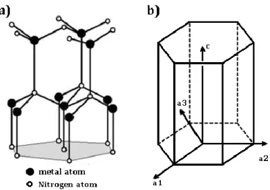
Group III-N namely AlN, GaN, InN and their ternary and quaternary alloys may occur in three different crystallographic structures. They may crystallize in wurtzite (hexagonal), zinc blende (cubic) and rock salt (cubic). The corresponding space groups are 𝑃63𝑚𝑐, 𝐹4̅3𝑚 and 𝐹𝑚3̅𝑚, respectively. The wurtzite configuration is the most stable at room temperature and atmospheric pressure, while the zinc blend and the rock salt are metastable[32,33]. In this manuscript only the wurtzite phase will be considered, it is exhibited in figure 1.1a. It is formed by two close packed hexagonal (hcp) sub-lattices of group III metals (Al, Ga, In) and group V (N), connected by a translation vector. The hcp unit cell is formed by 3 equivalent primitive unit cells where each atom occupies a tetrahedron site leading to 4 atoms per unit cell. The translation vector from the III to V atoms is 𝑢⃗ = (3 8)⁄ 𝑐 along the growth direction considered in this manuscript: 𝑐 = 𝑐[0001] where its modulus denotes the “c” lattice parameter. It is worth to mention that “u” represents the anion to cation distance and will depend on their respective radii.
The hexagonal basis set is formed by 𝑎 1, 𝑎 2, 𝑎 3 𝑎𝑛𝑑 𝑐 vectors as depicted in figure 1.1b. The vectors of the basal c-plan are 120° apart. 𝑐 is orthogonal to c-plan. For each direction a four indices (h, k, i, l) notation is assigned where 𝑖 = −(ℎ + 𝑘). This notation is useful to designate equivalent families of crystallographic plans and directions by exchanging the three first indices.
18
Figure 1.1: a) Wurtzite stacking of group III (Al, Ga or In) and group V (N) atoms of nitride semiconductors b) the hexagonal unit cell.
The lattice parameters of the three compounds AlN, GaN, and InN are given in table1.1[1]. As can be seen, in this materials family, where only the metal atom is changing from one compound to the other, any heterostructure growth along the c axis leads to a large mismatch as high as 13% in the case of growth of InN on AlN. This misfit is obtained using (1.1) relationship where 𝑎𝑓 and 𝑎𝑠 designate the film and substrate a-lattice parameter, respectively.
∆𝑎 =𝑎𝑓− 𝑎𝑠
𝑎𝑠 1.1
When ∆𝑎 > 0 , the layer is compressed to the substrate and when ∆𝑎 < 0 the layer is under tensile strain. For instance, when grown on GaN, AlN and InN would be under tensile and compressive strain, respectively.
Parameter [Å] AlN GaN InN Growth on GaN Mismatch
a0 3.1114 3.189 3.544 AlN -0.0243
c0 4.9792 5.185 5.718 InN 0.1113
Table 1.1: The lattice parameters of III -N compounds[1]. The misfit is calculated with respect to GaN.
1.2. Unit cell deformation: strain and stress
Geometrical modifications of the unit cell can be expressed by a tensor that links the primitive lattice vectors to a new set of basis vectors. It expresses normal and shear modification of the primitive unit cell due to, for example, the mismatch between lattice parameters or thermal expansion coefficients. If the original basis is defined by
19
an orthonormal set (𝑒 𝑥, 𝑒 𝑦, 𝑒 𝑧) and the modified one is (𝑒 𝑥′, 𝑒
𝑦′, 𝑒 𝑧′) then the strain tensor [𝜖𝑘𝑙] is given by (1.2): [𝜖𝑘𝑙] = ( 1 + 𝜀𝑥𝑥 𝜀𝑥𝑦 𝜀𝑥𝑧 𝜀𝑦𝑥 1 + 𝜀𝑦𝑦 𝜀𝑦𝑧 𝜀𝑧𝑥 𝜀𝑧𝑦 1 + 𝜀𝑧𝑧 ) 1.2
The coefficients 𝜀𝑘𝑘 represent the normal strain while 𝜀𝑘𝑙 represent the shear strain components. When no rotational modifications are involved, the strain tensor is symmetric.
Considering that the modification of the unit cell is due to a set of forces applied to the crystal then it can be described by a stress tensor [𝜎𝑖𝑗]. The above tensors are connected by the elastic constants(𝐶𝑖𝑗𝑘𝑙 ) as follows:
𝜎𝑖𝑗 = 𝐶𝑖𝑗𝑘𝑙𝜀𝑘𝑙 1.3
Due to the symmetry of [𝜖𝑘𝑙] the matrix form of the elastic tensor can be simplified in a contracted (6×6) symmetric matrix. The contraction can be obtained using the Einstein summation convention, thus each term of (1.3) can be written as:
𝜎𝑚 = 𝐶𝑚𝑛𝜀𝑛 1.4
Furthermore, it is helpful to consider the symmetry of the crystal to reduce the number of the independent elements of (𝐶𝑚𝑛 ). In the case of the hexagonal symmetry, this tensor can be written in the following form:
𝐶𝑚𝑛ℎ𝑒𝑥𝑎𝑔𝑜𝑛𝑎𝑙 = ( 𝐶11 𝐶12 𝐶13 0 0 0 𝐶12 𝐶11 𝐶13 0 0 0 𝐶13 𝐶13 𝐶33 0 0 0 0 0 0 𝐶44 0 0 0 0 0 0 𝐶44 0 0 0 0 0 0 𝐶66) 1.5
In the hexagonal system, this 6*6 matrix can take a simpler form, moreover, when the growth is carried out along the [0001] axis, the crystal does not experience stress along the z-axis, as it is free to expand or contract; and the deformation should be isotropic in the basal plane. These conditions lead to the following equalities:
𝜎33= 0;
20
𝜀11= 𝜀22= 𝜀𝑎
Hence, the strain-stress relationship becomes: (𝜎𝑎 𝜎33) = ( 𝐶11+ 𝐶12 𝐶13 2𝐶13 𝐶33) ( 𝜀𝑎 𝜀33) 1.7
Equation (1.7) can be expressed with an in-plane component and an out-of-plane component:
(𝜀𝑎; 𝜀33) = (𝜀∥; 𝜀⊥)
(𝜎𝑎; 𝜎33) = (𝜎∥; 𝜎⊥) 1.8
Taking into account that 𝜎33 = 0 , equation (1.7) with (1.8) becomes: 𝜀⊥= −2𝐶13
𝐶33𝜀∥ 1.9
In equation (1.9), 𝜀⊥ =𝑐−𝑐𝑐 0
0 , 𝜀∥=
𝑎−𝑎0
𝑎0 where (𝑎0, 𝑐0) and (𝑎, 𝑐) are respectively the
relaxed and strained lattice parameters and the term (−2𝐶13
𝐶33) is the biaxial term. The
relation (1.9) shows that, for instance, a layer under compressive in-plane stress will expand in the out-of-plane direction; this is known as the Poisson effect. For the in-plane case, the stress is related to the strain as follows:
𝜎∥= (𝐶11+ 𝐶12− 2 𝐶132
𝐶33) 𝜀∥ 1.10
The values of the elastic coefficients are given in table 1.2
Compound: AlN GaN InN C11[GPa] 396 367 223
C12[GPa] 137 135 115
C13[GPa] 108 103 92
C33[GPa] 116 405 224
Table 1.2: Elastic coefficient of binaries III -Nitrides[34]
1.3. Spontaneous and piezoelectric polarizations
In III-N compounds, one has to take into account the electronegativity of each Al, Ga, In and N; it is 1.61, 1.81, 1.78 and 3.04, respectively and it induces a displacement of the negative charges barycenter towards the N-atoms. Therefore, depending on the
21
crystal symmetry, charge dipoles can be present and the crystal exhibits spontaneous polarization at equilibrium.
For both wurtzite and zinc blende phases, each group III-atom is tetrahedrally bonded to nitrogen atoms. For the zinc blende, the stacking is …ABCABC… along the 4 symmetric [111] directions of the cubic system. Hence, the four dipoles are compensated by the four symmetric equivalent polar family planes <111> and no spontaneous polarization is present. In contrast, for the wurtzite structure, there is only one direction along which the stacking …ABAB… takes place; this direction is [0001]. Along this direction a spontaneous polarization at equilibrium (𝑝 𝑠𝑝) is always present. Therefore [0001] and [0001̅] are not equivalent as the group III-Nitrides have no inversion center. By convention, the polarity is defined by the vector pointing from the nitrogen atom to metal atom along the [0001]. Figure 1.2 shows Ga-polar case as projected along [112̅0] direction. In this instance the (𝑝 𝑠𝑝) points in the opposite direction of the [0001] growth directions.
Figure 1.2: Projection of Ga-polar of GaN wurtzite crystal observed along the [112̅0] direction[35].
In the case of the growth of a heterostructure, the lattice mismatch leads to the appearance of additional polarization. This polarization is known as piezoelectric polarization(𝑝 𝑝𝑧). For instance, a (𝑝 𝑝𝑧) can also appear in a zinc blende structure by carrying out the growth along one of the polar directions <111> which cancels out the symmetry along the growth direction as the dipolar momentum is no more compensated. In wurtzite, the growth of a heterostructure along [0001] direction with a lattice mismatch will strain the barrier creating a (𝑝 𝑝𝑧), this will reinforce or decrease (𝑝 𝑠𝑝) depending on the sign of the strain. Thus, the total amount of the
22
polarization will be the sum of the two contributions ([𝑃⃗ ] = [𝐶/𝑚2]). The consequence of the dipolar momentum is a specific charge distribution along the whole volume of a layer and the charge density is given by: 𝜌𝑣 = −𝑑𝑖𝑣(𝑃) . At the surfaces or interfaces, the excess electrical charges are given by: 𝜎𝑠𝑛⃗ = 𝑃𝑛⃗ where 𝑛⃗ is the normal vector pointing outside of the considered surface. For instance, III-polar surface of a bulk crystal will have a negative charge sheet (σ-) while N-polar surface will carry a positive charge sheet (σ+). Figure 1.3 shows the spontaneous polarizations in the case of a) relaxed and the appearance of the piezoelectric polarization in b) stressed GaN with a biaxial tensile strain. Figure 1.3c shows the case of AlN/GaN heterostructure for which AlN is under tensile strain to a relaxed GaN.
Figure 1.3: The spontaneous and piezoelectric polarizations in the case of a) bulk GaN, b) GaN under tensile strain and c) AlGaN/GaN
The values of the spontaneous polarization were calculated by Bernardini et al.[36] and are reported in table 1.3. More recently, Bechstedt et al.[37] showed that these constants are highly sensitive to infinitesimal changes in the crystal structure such as c/a ratio and bond lengths or even uncertainties in the structural parameters might change drastically the outcome of the simulations. In particular, InN and its alloys still lack reliable experimental data, thus the interpretation of its behavior may still be controversial. The piezoelectric polarization can be determined from the piezoelectric tensor of the corresponding space group. For the wurtzite symmetry P63mc space group, it is as follows:
23 𝑝𝑝𝑧 = ( 0 0 0 0 𝑒15 0 0 0 0 𝑒15 0 0 𝑒31 𝑒31 𝑒33 0 0 0 ) ( 𝜀11 𝜀22 𝜀33 𝜀23 𝜀13 𝜀12) 1.11
Where eij are the piezoelectric elements of the tensor, εkk are the uniaxial strain elements and εkl (with k≠l) are the shear strain elements. The values of eij are also reported in table 1.3. Considering the absence of shear and only the biaxial strain for the growth along [0001], (1.11) can be combined to (1.09) to become:
𝑝𝑝𝑧[0001] = 2𝑎 − 𝑎0
𝑎 (𝑒31− 𝑒33 𝐶13
𝐶33) 1.12
In devices such as HEMTs, the polarization is of primary importance as it impacts the density of the carrier and the mobility of the 2DEG. In wurtzite symmetry materials, the piezoelectric polarization is one order of magnitude higher than in zinc blende materials and a large spontaneous polarization is indeed present[38].
Compound: AlN GaN InN Psp [C/m2][39] -0.09 -0.034 -0.042 e33[C/m2][36] 1.46 0.73 0.97 e31[C/m2][36] -0.6 -0.49 -0.5
Table 1.3: Spontaneous polarization and piezoelectric coefficients of the III-Nitrides
1.4. Properties of AlInN and AlGaInN alloys
Conventionally, many properties of an alloy like the bandgap energy or lattice parameters can be calculated using a linear combination of those of the parent compounds, and this is known as the empirical Vegard’s law. Considering that α and β are the binaries with 𝑥 the mole fraction of α, then the desired property is extracted from a linear equation (1.13) for a ternary alloy.
Υ(𝑥) = 𝑥Υα+ (1 − x)Υβ 1.13
Where Υ is the unknown physical property, for a quaternary alloy (1.13), it becomes:
Υ(𝑥, 𝑦, 𝑧) = 𝑥Υα+ yΥβ+ zΥδ 1.14
In (1.14) y and z are the mole fractions of β and δ binary compounds with x + y + z = 1.
24
The applicability of the linear form is controversial since deviations are often reported. Using ab initio density functional simulations (DFT), Bernardini et al.[39] showed that for AlInN, the spontaneous polarization and thus the macroscopic polarization exhibits a large deviation from linearity. The deviation is taken into account by the introduction of a non-linear term to the Vegard’s law. This macroscopic deviation has been attributed to the microscopic hydrostatic stress and internal strain due to chemical ordering[39,40]. Thus for the spontaneous polarization (1.13), the above authors proposed:
𝑝𝑠𝑝(𝑥) = 𝑥𝑝
𝛼𝑠𝑝+ (1 − 𝑥)𝑝𝛽𝑠𝑝+ 𝑏𝑠𝑝,𝛼𝛽𝑥(1 − 𝑥) 1.15
Where 𝑏𝑠𝑝,𝛼𝛽 is the deviation from linearity and it is also called “bowing parameter”, for the ternary alloys (AlInN, InGaN and AlGaN), they calculated 0.071 C/m² 0.037 C/m² and 0.019 C/m² respectively [39]. On the same basis, equation (1.14) becomes for a quaternary alloy [38]:
𝑝𝑠𝑝(𝑥, 𝑦, 𝑧) = 𝑥𝑝
𝛼𝑠𝑝+ 𝑦𝑝𝛽𝑠𝑝+ 𝑧𝑝𝛿𝑠𝑝+ 𝑏𝑠𝑝,𝛼𝛿𝑥(1 − 𝑥) + 𝑏𝑠𝑝,𝛽𝛿𝑦(1 − 𝑦) + 𝑥𝑦(𝑏𝑠𝑝,𝛼𝛽 − 𝑏𝑠𝑝,𝛼𝛿− 𝑏𝑠𝑝,𝛽𝛿)
1.16
In 2003, Voznyy et al.[40] calculated the bandgap bowing energies for III-N ternaries using pseudo-potential simulations; they reported that AlInN has the largest value of 3.62 eV in comparison to AlGaN and InGaN (0.3 eV and 1.89 eV, respectively). Later that year, Dridi et al.[41] reported similar values for InGaN and AlGaN but for AlInN their calculation based on DFT leads to reevaluating it at 4.09 eV. In 2006, Terashima et al.[42] reported that the bandgap bowing might approach 4.96±0,28 eV. As also suggested by Gorczyca and coworkers[43–45] between 2009 and 2011, the higher values of this bowing are characteristic of indium-containing alloys. They suggest a quadratic compositional dependence of the bandgap bowing for both ternary AlInN and then quaternary AlGaInN alloys that takes into account indium clustering. In this instance, a uniform alloy AlInN has its bowing parameter from 2.1 eV to 6.2 eV (4.4 eV for 50% indium content) whereas the model taking into account the indium clustering AlInN has its bowing parameter ranging from 3.9 eV to 14 eV (8.6 eV for 50% indium content).
25
Regarding the lattice parameters “a” and “c”, Darakchieva et al.[46] reported, using ab initio calculations, that both (a,c)-lattice parameters exhibit a deviation from the linear form and proposed the following bowing parameters: b𝑎 = 0.0412 ± 0.0039 Å 𝑎𝑛𝑑 b𝑐 = −0.060 ± 0.010 Å. Subsequently, the same group [47] reported that using the above parameters, one may have consistency between x-ray diffraction (XRD) and Rutherford back scattering (RBS) experiments. However, they have pointed out that a perfect agreement might not be achieved due to non-random distribution of indium atoms, the possible contamination with gallium atoms (up to 2%) or to the presence of defects.
Therefore, the physical properties of InN are still under constant discussion in the field. In fact, from 1994 to 2017, the in-plane lattice parameter “n” of this binary went from 3.548 Å[32] to 3.544 Å[1]. However, in 2002, Davydov et al.[48] reported that aInN= 3.5365 Å from X-ray analysis. Later, in 2006, GaN et al.[49] optimized from first principal calculation the a-lattice parameter of InN around 3.518 Å. Considering the ternary alloy, while using the lattice parameters of the binary compounds provided in ref.[1] and by applying Vegard’s law without deviation, the lattice match of Al1-xInxN/GaN is for 18% of indium content. Furthermore, if the deviation from Vegard’s law is taken into account as suggested by Darakchieva et al.[46], then a lattice parameter of 3.189 Å (a-GaN) is obtained at 19.5% of indium content. Moreover, for the quaternary alloy, the solution can be obtained by any triplet (x, y, z) satisfying the unmodified equation 1.14. Thus, for both ternary and quaternary alloys, the determination of a physical property depends on the knowledge we have on the properties of the end binary compounds.
1.5. Structural defects in III-Nitrides
Crystalline materials exhibit mostly point, line and planar defects[50]. The efficiency of devices is critically dependent on the density of these defects which can be present in the processed material needed for their fabrication. It is therefore important to study them in order to understand their structure, chemistry and formation mechanisms, and eventually help to grow better quality materials for optimized devices performance.
26
1.5.1. Point defects
In a perfect crystal, atoms occupy specific crystallographic sites, however, due to many reasons; a number of such sites may not be occupied, which gives rise to vacancies. The atoms can also be located out of these specific sites, thus becoming interstitial impurities. Moreover, the purity of materials is never 100%, foreign impurities are incorporated during the synthesis, and such foreign impurities may occupy the specific atomic sites of the material, in which case they are called substitutional impurities, or be located at interstitial sites. Kim et al.[51] carried out the growth of Si-doped GaN. The authors correlated the concentrations of silicon and oxygen impurities while increasing the ammonia flow rate; they reported a decrease in the Hall mobility when the impurities concentration is increased. Similarly, Fang et al.[52] reported an increase in nitrogen vacancies in Si-doped GaN grown by reactive molecular beam epitaxy (r-MBE) when the temperature is lower than 800 °C. Thus the concentration of impurities may lead to a change in the doping and/or the mobility of the carriers. In contrast, Li et al. [53] by density functional theory (DFT) showed that gallium interstitial might enhance the yellow luminescence which is an impurity level often present in photoluminescence spectra of GaN films.
1.5.2. Dislocations
Dislocations are line defects in crystals that are characterized by a line direction (l) and a displacement vector known as the Burgers vector induced inside the crystal along the line. When the Burgers vector is a linear combination of lattice vectors the dislocation is called entire, and when it corresponds to a fraction of a lattice parameter, the dislocation is said to be partial[54]. As the dislocation is completely defined by its line (𝑢⃗ ) and Burgers vector (𝑏⃗ ), the geometrical relationship between the two vectors determines the type of the dislocation. The dislocation is of screw or edge type when 𝑢⃗ and 𝑏⃗ are parallel or perpendicular, respectively, otherwise, it is of mixed type. Figure 1.4 shows the two types of dislocations, in a cubic symmetry material.
27
Figure 1.4: a) Representation of an edge dislocation. The red inverted T -shape shows that the dislocation line is out of the plane (MNOP) and is perpendicular to its Burgers vector b) Representation of a screw type dislocation in a 3D view. The red line shows that
the dislocation line and its Burgers vector are parallel [55].
An edge dislocation can be formed by inserting a half-plane in the crystal. The dislocation line position is at the end of this additional plane as shown in figure 1.4a by an inverted red “T” and its Burgers vector is orthogonal to the dislocation line. A screw dislocation can be generated by pushing half of the crystal along a particular line by an amount of the lattice parameter as depicted in figure 1.3b. In this case, the dislocation line (shown with a red line) and the Burgers vector are parallel. A general dislocation of mixed type has an edge and a screw component.
In the hexagonal lattice, as encountered in nitride materials, a perfect dislocation can have “𝑎 ”, “𝑐 ” and “𝑎 +𝑐 ” as possible Burgers vectors. As an example, let’s consider the 𝑎 dislocation, if its line is located in the basal plane, it can be of edge or mixed type. When the line is along [0001], it is of edge type. In that case, it propagates from the interface of epitaxially grown layers towards the layer surface and it is referred to as 𝑎 threading dislocation (TD). In the same geometry, the 𝑐 dislocation is of screw type and 𝑎 +𝑐 type is a TD of mixed type. Table 3 summarizes common dislocations and their Burgers vectors. The partial dislocation in the 13[101̅0] is called the Shockley partial and note as “p”.
28
Dislocation character Symbol Burgers vector
perfect a 1 3[112̅0] perfect a [0001] perfect a+c 1 3[112̅3] Partial (Shockley) p 1 3[101̅0] Partial (Frank) c/2 1 2[0001] Partial (Frank-Shockley) p+c/2 1 6[202̅3]
Table 1.3: Dislocations and their burgers vectors in the close-packed hexagonal system
with Miller-Bravais notation
The impacts of dislocations on devices are various. For instance, Jena et al. [56] showed theoretically that the mobility of the 2DEG in a HEMT structures such as AlGaN/GaN can be strongly decreased with increasing the dislocation density. In this instance, Kotani et al.[57] observed a reduction by up to four orders of magnitude of the leakage current measured at the gate Schottky contact of an AlInN/AlN/GaN HEMT whenever the dislocation density is decreased from 1.8×104 cm-2 to 1.2×109 cm-2.
1.5.3. Planar defects
A planar defect is present when the crystal periodicity is interrupted along a well-defined plane through a displacement (translation) or a more complex combination of group symmetry operations. Planar defects can be stacking faults (SF), inversion domains boundaries (IDB) and grain boundaries (GB). They are described by the interrupted symmetry operation that connects the two sides of the crystal limited by the boundary.
Stacking Faults
Focusing on the wurtzite lattice, the SFs are classified into three types: intrinsic I1, intrinsic I2 and extrinsic E. In terms of formation energy, it increases in the presented order[58]. These two-dimensional defects can be represented as quantum wells leading to radiative recombination of excitons in GaN[59]. Therefore they can be characterized by luminescence spectroscopy. Furthermore, these defects can change the local stacking from wurtzite to zinc-blende which is the case of I1 leading to a modification of the local polarization and thus affects the carrier density[60]. I1 can be obtained by the introduction of a zinc-blende row stacking in the wurtzite sequence
29
along [0001]. In terms of crystal symmetry, it is obtained by removing one plane (basal plane) and then applying a shear by 13[101̅0] thus the final displacement vector is 16[202̅3]. For instance along [0001] and for a [112̅0] projection, the stacking is modified from …AaBbAaBbAaBb… to …AaBbAaCcAaCc… I1 is not obtained from dissociation of dislocations, thus, this defect is a growth defect. I2 can result from a shear in the basal plane that introduces two rows of zinc-blende or the dissociation of an “a” type dislocation into two partial Shockley dislocations thus the fault vector is 13[101̅0]. The new stacking is then …AaBbAaBbCaAaCaAa…. E fault is obtained by the addition of a plane in the cubic position in the hexagonal stacking. Therefore, the stacking becomes …AaBbAaBbCcAaBbAaBa… and has a fault vector of 12[0001].
Inversion domains
A real crystal may be formed by a number of more or less disoriented grains separated by boundaries. The junction between the single crystals is called a grain boundary and the two sides of a boundary can be related by different symmetry operations such as rotation, inversion or mirror[61]. In non-centrosymmetric materials, such as the wurtzite III-Nitrides, a particular planar defect can be an inversion domain (ID) boundary (IDB), when the two sides of the crystal are related to the inversion operation which can be pure or combined with a translation.
31
2 Characterization techniques
This chapter describes the main characterization techniques used in this investigation of AlInN and AlGaInN layers. The first observations of all the samples were systematically carried out with atomic force microscopy (AFM). In parallel, specimens were prepared for transmission electron microscopy either by mechanical polishing or when necessary by focused ion beam (FIB). Scanning electron microscopy (SEM) observations were also made in the FIB facility. Therefore specific sites and defects identified by AFM were extracted for TEM analysis. Atom Probe Tomography (APT) was also performed.
2.1. Atomic force microscopy
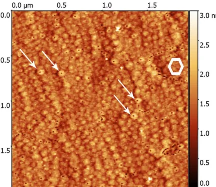
Subsequent to the invention of scanning tunneling microscope (STM) by Binning and Rohrer ( Nobel Prize 1983)[62]the AFM which uses forces instead of the electric tunneled signal came up to permit the investigation of non-metallic surfaces.
In the AFM, a sharp probe is attached to an oscillating cantilever. The end radius of the probe is typically between 5 nm and 15 nm. When, the probe is approached to the surface of the sample an interaction force appears, this force depends on the distance between the tip and the material surface properties.
There are three different modes in AFM. If the tip is in contact with the surface of the material, then it is operating in a repulsive regime and corresponds to a Coulomb interaction. When the tip is few nanometers far from the surface, the probe goes in an attractive regime toward the surface. In this case, a Van Der Waals interaction is observed. For the characterization of our layers, we have used the third mode which is called tapping mode. In this semi-contact mode, the cantilever is firstly set to oscillate at its free resonance frequency when the cantilever is far from the sample surface. During the approach of the oscillating cantilever towards the surface, the free amplitude decreases near the surface. Therefore, an amplitude setpoint is chosen (which is usually ~70% of the free oscillation amplitude) to define the strength of interaction between tip and sample. Under this operating condition, the topography is obtained. Figure 2.1 shows the force-distance dependence curve.
32
Figure 2.1: Force-distance curve dependence. In a repulsive regime, the t ip is in contact with the surface. If the tip is few nanometers away from the surface Van Der
Waals interaction is felt[63].
In the AFM, piezo-ceramics are controlling the fixed amplitude set point which is used as a feedback for the z-displacements. The scanning can be performed by either moving the tip or the sample with respect to each other. Any variation of the interaction force between the tip and the surface from the set point (constant amplitude) will be detected by a laser beam. This laser points to the edge of the cantilever and is reflected back to a photodiode. The plot of the laser deflection versus the position on the surface gives the topography of the probed region. From this height image, the standard deviation of the amplitude gives the average roughness of the surface.
2.2. Electron microscopy
Transmission Electron microscopy (TEM) and scanning electron microscopy (SEM) were used to investigate the specimen properties from different aspects.
2.2.1. Scanning electron microscopy
The SEM is a characterization technique that provides information on surface state, morphology, and orientation maps can be obtained by Electron Backscattered Diffraction (EBSD). The composition is measured by energy dispersive spectroscopy (EDS). In this work, we used the dual beam FEI Nanolab (SEM/FIB) for the SEM observations and mainly for specimen preparation.
33
2.2.2. Transmission electron microscopy
Transmission electron microscopy[64] offers a broad range of observations and analysis techniques. During this thesis, TEM was extensively used as the main characterization technique. The samples investigated in this work were prepared as cross sections and plan views. In such instruments, one can reach the atomic resolution in imaging and chemical analysis. Therefore it is possible to determine with a high accuracy the composition of a given sample, its crystallographic properties, and defects in the observed areas….
The transmission electron microscope is composed of an electron source operating at few tens to hundreds of keV. This cathode is often called a filament; it can operate at high temperature, or without heating for more coherence. Along the path of the electrons, electromagnetic lenses provide the investigator different imaging and diffraction modes for the analysis of the samples which need to be transparent to these energetic electrons. In the TEM, several diaphragms are there to select either a zone of interest or for shaping the electron beam. Diaphragms are placed in different eigen plans. The images and diffraction patterns are obtained in specific planes along the instrument column, they reflect the interaction of the high energy electron beam with the material under investigation.
Three JEOL TEMs have been used in this work all operating at 200 keV: 1) The JEOL-2010 conventional TEM with a stage that allows sample tilting up to +- 40° was used to investigate the microstructure of our materials using diffraction contrasts. In this microscope, the electron source is a thermionic LaB6 crystal. 2) The second instrument is a JEOL 2010 equipped with a Field Emission Gun (FEG). This microscope was mainly used in scanning mode (STEM). In the annular dark field (ADF) mode, using small camera lengths, it allows Z-contrast images of our heterostructures, although due to the optical quality of this instrument, atomic resolution cannot be attained. Most of the EDS analysis was carried out on this instrument in STEM mode. For improved spatial and spectrometric resolution, we also had access to the ARM 200 in Caen.
Due to the limited access to the ARM in Caen, a number of experiments were also carried out either on the FEI TITAN operating at 300 keV at the Institute of Solid State
34
Physics, BREMEN, Germany, as well as at the Institute of Physics Warsaw, and on the ARM 200CF of the Max Planck Institute, STUTTGART, Germany.
2.2.3. Electron sources and electron guns
The electron sources (the cathode) can be classified into two types: thermionic and field effect sources. Tungsten (W) and LaB6 crystals are usually used as electron sources.
a- Thermionic sources
Heating materials such as tungsten and LaB6 can give to the electrons enough energy to leak from the surface of the considered crystal source. In a microscope, the gun is maintained under vacuum and at an accelerating voltage so that the extracted electron can travel to the sample at the set energy.
The extraction energy “Φ [eV]” is known as the work function of the material from which the electrons are extracted. Richardson’s law gives a good approximation of the electron emission theory. The following equation gives the relationship between the current density “J [A.m-2]” to the operating temperature “T [K]”:
𝐽 = 𝐴𝑇²𝑒− Φ𝑘𝑇 2.1
Where “k = 8.6⨯10-5 eV.K-1” is Boltzmann constant and “A [A.m-2.K-2]” is Richardson’s constant and depend on the used source. Formally speaking, in order to obtain a current density, one has to achieve the following condition: kT > Φ. The source can be tungsten (filament) for its high melting point around 3400 °C. In practice, LaB6 (crystal) which has a lower extraction work function around 2.4 eV in comparison to tungsten (4.5 eV) with a tip radius less than 1 µm results in a higher current density and a brightness 10 times stronger than for tungsten. For this smaller source size, a more coherent beam is formed along with less scattered electron energy dispersion (1 eV – 1.5 eV). Therefore LaB6 filaments are employed as thermionic sources. Figure 2.2 is a schematic representation of a thermionic source.
35
Figure 2.2: Schematic diagram of a thermionic electron gun. A high voltage is applied between the cathode and the anode. The Wehnelt is the first electrostatic lens that the electrons go through in the TEM. Its electric field focuses the electrons into a crossover
“d0” with a convergence/divergence angle α0 which is the true source (object) for the lenses in the TEM illumination system[64].
b- Field effect sources
A field effect gun (FEG) emission is governed by the electron tunneling theory. In this instance, a monocrystalline material is shaped as a tip and is submitted to a high extraction potential and is under vacuum. At the apex of the tip, electrons can tunnel out following the equation (2.1):
𝐸 = 𝑉
𝑟 2.2
Here “r” is the tip radius. For instance, if r = 100 nm then E= 1010 V/m, (for an applied voltage of 1kV). In contrast to a thermionic emission where the temperature plays an important role, in the case of the field emission the vacuum needs to be very low (10-10-10-11 Torr) to avoid tip contamination and allow the electrons to tunnel out. Two methods are currently used in modern FEG TEMs 1) the extraction at room temperature; this type of source is called cold FEG and offers a highly coherent beam.

![Figure 3: The possibilities that offer AlGaInN alloys in terms of the lattice parameters, bandgap, and polarization matches while grown on (000 1)-GaN[23]](https://thumb-eu.123doks.com/thumbv2/123doknet/12863025.368696/23.892.211.726.101.624/figure-possibilities-algainn-lattice-parameters-bandgap-polarization-matches.webp)

![Figure 2.8: Comparison between a parallel illumination and a convergent beam resulting in diffraction disks of a CBED pattern [67]](https://thumb-eu.123doks.com/thumbv2/123doknet/12863025.368696/55.892.274.674.111.379/figure-comparison-parallel-illumination-convergent-resulting-diffraction-pattern.webp)
![Figure 2.9: Schematic showing the principle of the APT process . With modifications from [71]](https://thumb-eu.123doks.com/thumbv2/123doknet/12863025.368696/57.892.168.760.461.763/figure-schematic-showing-principle-apt-process-modifications.webp)

![Figure 3.3: Schematic view of the close-coupled shower-head MOVPE facility[72]](https://thumb-eu.123doks.com/thumbv2/123doknet/12863025.368696/62.892.189.730.222.445/figure-schematic-view-close-coupled-shower-movpe-facility.webp)