Advanced Applications in Wide-Area Impedance Sensing
by
Elizabeth C. George
S.B., Massachusetts Institute of Technology (2012)
Submitted to the Department of Electrical Engineering and Computer Science
in partial fulfillment of the requirements for the degree of
Master of Engineering in Electrical Engineering and Computer Science
MASSACNUSETTS INGT TUTE
at the
j
OF TECHNOLOGYMASSACHUSETTS INSTITUTE OF TECHNOLOGY
JUL
15
2014
February 2014
1LIBRA.RIES
@
Massachusetts Institute of Technology 2014. All rights reserved.
Signatu
A uthor ...
....
Depar~ent of
Certified by..
Certified by...
re redacted
' ...
..
:...
Electrical Eng eering and Computer Science
January 31, 2014
Signature redacted
... ...
Dr. Steven B. Leeb
Professor of E.E.C.S. & M.E., MacVicar Faculty Fellow
4-.
A
4
A
Thesis Supervisor
gnar
U
rc
C ac.#LCU
... ...
Al-Thaddeus Avestruz
Doctoral Candidate
Thesis Supervisor
Signature redacted
Accepted by...
...
Prof. Albert R. Meyer
Chairman, Master of Engineering Thesis Committee
....
Advanced Applications in Wide-Area Impedance Sensing
by
Elizabeth C. George
Submitted to the Department of Electrical Engineering and Computer Science on January 31, 2014, in partial fulfillment of the
requirements for the degree of
Master of Engineering in Electrical Engineering and Computer Science
Abstract
In this thesis a wide-area impedance sensor used in hyperspectral imaging for a wide variety of ap-plications is presented. Building on previous work, this sensor is decoupled from fluorescent lamps and thus is used to passively detect independent sources such as fluorescent lamps and laptop con-trol signals. The active sensing electrodes with common-mode feedback are used with a spectrum analyzer and synchronous demodulator for source and material detection respectively. A setup for active source multiplexing is described and used in image reconstruction and material detection. Algorithms for image reconstruction from such ill-posed inverse problems are discussed and improve-ments are made. Hyperspectral techniques for extracting the occupancy values of various materials are shown. Finally, future experiments using this sensor for gesture sensing and as a purely digital demodulator for passive imaging are described.
Thesis Supervisor: Dr. Steven B. Leeb
Title: Professor of E.E.C.S. & M.E., MacVicar Faculty Fellow Thesis Supervisor: Al-Thaddeus Avestruz
Acknowledgements
I would like to thank everyone whose support made this thesis possible. I am extremely grateful
to my thesis supervisors, Professor Steven B. Leeb and PhD Candidate Al-Thaddeus Avestruz, for
their continued guidance and wisdom. I would also like to thank my colleagues from LEES and
friends at MIT for their help and encouragement. They include, but are not limited to, Shahriar
Khushrushahi, William Thompson, Brian Sennett, Kawin (North) Surakitbovorn, Arthur Chang,
John Donnal, Jim Paris, Shuyi James Chen and Ashley Brown.
I would finally like to thank my family, especially my parents Christine and Dan George, for
their constant support throughout my time as an undergraduate and graduate student, and beyond.
Contents
1 Introduction
15
1.1 Motivation . . . . 15 1.1.1 Performance objectives. . . . . 15 1.1.2 Applications . . . . 151.2
Previous Work . . . .
16
1.3 Thesis Overview . . . . 172 Sensor Circuitry and Setup 19 2.1 Overview . . . . 19
2.2 High Voltage Source . . . . 20
2.3 Sensing Circuitry . . . . 21 2.3.1 Front-end Amplifier . . . . 21 2.3.2 Signal Conditioning . . . . 23 2.4 Circuit Changes . . . . 26 2.4.1 Signal Conditioning . . . . 26 2.4.2 Signal Synthesis . . . . 27
2.4.3
HV Selection . . . .
27
2.5 Setup ... ... ... . ... . .. ... 29 3 Passive Scanning 31 3.1 Analog Demodulation . . . . 31 3.2 Spectrum Analyzer . . . . 32 3.3 Applications . . . . 33 4 Hyperspectral Imaging 39 4.1 Background ... .. ... ... ... ... ... 39 4.2 Previous Work . . . . 405 Imaging Techniques 5.1 Setup .... ... 5.2 T heory . . . . 5.3 Forward Problem . . . . 5.4 Inverse Problem . . . . 5.4.1 Constraints . . . .
5.4.2
CV X . . . .
5.5 Image Reconstruction Algorithms . . . .5.5.1 Linear Back Projection . . . .
5.5.2 Least Norm . . . .
5.5.3 2-Norm with 2-Norm Regularization
5.5.4 1-Norm with 2-Norm Regularization
5.5.5 2-Norm with 1-Norm Regularization
5.5.6 Landweber/Newton-Raphson .
5.5.7 Image Segmentation . . . .
5.6 Improvements . . . .
5.6.1 Influence Matrix . . . .
5.6.2 Subpixel . . . .
6 Occupancy Detection Results and System Performance 6.1 Sensor Range . . . .
6.2 Noise and Drift . . . .
6.3 Object Detection . . . .
6.3.1
Scalability of Objects . . . .
6.3.2 Multiple Materials . . . .
7 Conclusion and Future Work
7.1
Sum mary . . . .
7.2
Future Work
. . . .
7.2.1
Electrode Configurations . . . . .
7.2.2
Digital Demodulation . . . .
7.2.3
Laptop Gesture Sensor . . . .
7.2.4
Floor Shoe Scanner . . . .
A Code
A.1 Sensor Interfacing Software in
43
43
. . . .
43
. . . .
46
. . . .
49
. . . .
49
. . . .
50
. . . .
50
. . . .
50
. . . .
52
. . . .
53
. . . .
53
. . . .
53
. . . .
54
. . . .
54
. . . .
55
. . . .
55
. . . . 5657
57
57
58
59
60
63
63
64
64
64
64
64
65
65
A.1.2 recorder.m
. . . .
66
A.1.3 rangeExpt.m . . . . 67 A.1.4 lightpulse.m . . . . 70 A.1.5 gridExpt.m . . . . 72A.1.6 BM atrix.m . . . .
78
A.1.7 AM atrixPM .m . . . .
79
A.1.8 ImSeg.m . . . .
83
A.2 Sensor Board Software . . . . 85
A.2.1
FullyDiff8.c . . . .
86
B Schematics and Boards 103 B.1 High Voltage Signal Source . . . . 104
B.1.1
Full Schematic . . . 104
B.1.2 PCB Layout . . . 105
B.1.3 Bill of M aterials . . . . 106
B.2 Standalone Sensor Electrodes . . . . 107
B.2.1 Capacitive M ode Electrodes . . . . 107
B.2.2 Resistive Mode Electrodes . . . . 111
B.3 Sensor Signal Conditioning . . . . 115
B.3.1 Full Schematic . . . . 115
B.3.2 PCB Layout . . . . 128
B.3.3 Bill of M aterials . . . . 129
B.4 Atmega32U4 Breakout Board . . . . 131
B.4.1 Full Schematic . . . . 131
B.4.2 PCB Layout
. . . .
132
List of Figures
2-1 A lumped element model for the capacitive sensor system [1]. . . . . 19
2-2 Diagram of the generalized standalone occupancy sensor. . . . . 20
2-3 The circuit model for the PI controller and plant. vi, is taken from the output of the
multi-frequency source from the sensor board and v0,t drives the source plates directly. 20
2-4 The high voltage source board. . . . . 21
2-5 These figures were taken from a single frame of a digital oscilloscope. . . . . 22
2-6 A close-up of the front-end amplifier on one of the receive electrodes. . . . . 23
2-7 Schematic for the half circuit common mode feedback of the front end amplifier. Feedback capacitances represent lumped T-networks. Electrode circuitry is left of the cable and sensor board circuitry to the right. . . . . 24
2-8 Block diagram for the common mode feedback of the front end amplifier. . . . . 24
2-9 The generalized block diagram for the signal conditioning circuitry. The first gain stage is singled ended and located on each respective electrode. The following stages are all fully differential and reside on the sensor board. The dashed box is replicated four tim es. . . . . 25
2-10 One-channel circuit implementation of the synchronous demodulator. . . . . 25
2-11 The sensor board with DDS signal creation in the bottom-right corner, microcontroller breakout in the center-right and demodulation signal creation top-right. The front-end amplifier is at the input to the board on the left. The signal is delivered to the board from the active receive electrodes via driven coaxial cables to the MMCX connectors. ... ... 26
2-12 Schematic for one channel of the high voltage source multiplexer board. Three relays are stacked in series to standoff the 500 V peak voltage. The remaining two channels and shield switches are not shown. . . . . 27 2-13 Revision 2.0 of the high voltage multiplexer board. Large separation between channels
2-14 Receive electrodes placed on plastic shelves in the lab space. Sensor electronics are
beyond the shelves on the ground and source electrodes are on a table across the lab
space. ...
...
29
3-1
Block diagram of manual demodulation tuning test. . . . .
32
3-2 Gradually increasing the demodulation frequency to within 0.01 Hz of the independent
source frequency. ...
...
32
3-3 With the demodulation frequency within 0.01 Hz of the source frequency, the beat
frequency is observed over time. . . . .
33
3-4 Block diagram of manual demodulation tuning test. . . . .
33
3-5 These figures were taken from a single frame of the spectrum analyzer used with our
front-end amplifier and electrodes.
. . . .
34
3-6
These figures were taken from a single frame of the spectrum analyzer used with our
front-end amplifier and electrodes. The laptop was placed on the same shelf as the
left-side electrode.
. . . .
35
3-7
These figures were taken from a single frame of the spectrum analyzer used with our
front-end amplifier and electrodes.
. . . .
36
4-1 The conductivity and permittivity of human muscle as a function of frequency [2,3].
39
4-2 The conductivity of aluminum as a function of frequency.
. . . .
40
4-3 Difference between COMSOL-modeled human image at 100kHz and 20kHz . . . . .
40
4-4 A COMSOL-modeled test case distribution with solutions by the LBP and SVD
algorithm s.
. . . .
41
4-5 The same test case distribution with solution by the Landweber algorithms. . . . . .
41
4-6
The experimental setup and test case for hyperspectral ECT. In this test case, pixels
1 and 4 were filled with water and pixels 2 and 3 were filled with wood. On the right,
the difference between the permittivity distributions at 10kHz and 100kHz. . . . . .
42
5-1
The 4x4 grid in 2D space used as the spacial reference for all imaging. . . . .
44
5-2 Partial image of the 4x4 floor grid used for all experiments. . . . .
44
5-3 On the left, individual pixels are filled with dielectric material to calculate the values
of the sensitivity matrix. On the right, the result of the superposition of all pixels is
shown...
...
46
5-4 A pictorial representation of the linear back-project algorithm for "hard-field"
tomo-graph ies. . . . .
51
5-5
Fitting data for measurements taken at each pixel in 13x13 grid: source position 1,
6-1 The response of the sensor as a single source electrode is moved away from the receive
electrodes. . . . . 58 6-2 The relative difference between the levels of human material calculated by the 11
algorithms with 11 regularization for two people of different sizes. . . . . 60
6-3 Occupancy values in the 4x4 gridspace with two people differentiated by size. . . . . 61
6-4 The occupancy maps of human and metal presence in the lab space. In this case, noise-free data is used in the sensitivity calibration and as the experimental data and a perfect detection is achieved. . . . . 62
List of Tables
2.1 Stray capacitance measurements at 100kHz . . . . 28
3.1 Lab Space Independent Source List . . . . 37
6.1 Noise Floor Measurements . . . . 59
6.2 Repeated Calibration Data . . . . 59
6.3 Multiple Object Data Pairs . . . . 59
Chapter 1
Introduction
1.1
Motivation
1.1.1
Performance objectives
The need for a simple, cheap occupancy detector and material detector has motivated the research
presented in this thesis. This sensor would take precise differential current measurements to create an
accurate depiction of the material occupancy of a given space through the use of image reconstruction
algorithms. The sensor's low SNR would make it possible to reconstruct an image of a resolution
relevant to the size of an average person.
1.1.2
Applications
Several possible applications are envisioned and detailed here. Airport body-image scanners have
un-dergone many changes in recent years, first due to legislation mandating increased security measures
at airport checkpoints following the 9/11 terrorist attacks. The introduction of full-body scanners
was followed quickly by backlash from privacy groups likening the scanners to a "virtual strip search"
with many also fearing the effects of the scanners' radiation. Many called for new legislation to
pro-tect them from such invasive technologies [4]. The capacitive sensing system described in this paper
could be used to replace existing airport x-ray scanners to provide a minimally invasive alternative
which would pick up the presence of metals, suspicious plastics used in making explosives, and other
dangerous substances.
One of the biggest areas of development in Human Interface Devices (HIDs) is in gesture
recog-nition. Capacitive touch sensor with multi-touch capabilities have been realized in many commercial
products including mousepads, smartphones and touchscreens. The research focus has shifted
to-wards methods of sensing without maintaining physical contact between the user and the device
[5].
This idea is quite new, with only a few products currently out in the market boasting this technology.
However, the current implementation which requires a dedicated camera and significant processing
power could greatly benefit from integration with a low-power solution.
A touchless capacitive gesture recognition system installed on a 12" laptop screen was proposed
and built in 2006 [6] using four long metal electrodes arranged around the screen's bezel. This system
was only capable of differentiating a few gestures, with low reliability. A similar system for low cost
gesture sensing on the centimeter scale was demonstrated in 2011 [7]. Another simple touchless
capacitive user interface using an array of small electrodes in a row to track user movement has
been implemented for use in interactive textiles for patient care [8]. Combining these technologies,
a screen using multiple arrays of electrodes around its keyboard and screen could provide refined
tracking and a larger range of gestures supported. This sensor's unique ability to distinguish between
different types of materials present in an area using hyperspectral detection has not been realized
in its current applications, and will be discussed here.
Standard room sensors detect motion, not occupancy, and cannot differentiate between the
pres-ence of a human or other objects. This sensor would present a great improvement over standard
room detectors as it could tell the relative occupancy level of a space and would be able to detect
hu-man presence when stationary. The goal of this sensor is to be able to distinguish between different
objects and materials.
To obtain detailed information about the usage of potentially inefficient loads on a utility network
can be a hard problem. Smart-metering technologies can be expensive when sensors must be installed
to monitor every load in a network. Non-Intrusive Load Monitoring (NILM) is a proposed solution
to the smart-metering problem which inserts one sensor into a network and uses smart processing
to differentiate loads from one-another. A passive capacitive scanner which takes the frequency
signature of a space with a very high frequency could perform this task in a
load-saturated
area. The
passive scanner is an exciting tool that can amplify the signals present in a room (from fluorescent
lamps to monitors refreshing) and use these signals to detect objects in the space.
1.2
Previous Work
The first iterations of this sensor were electrically coupled to fluorescent lamps. Electrodes on the
lamp would synchronously detect changes in the electric field produced by the excitation of the
fluorescent ballast and use this information to detect human presence [9,10]. The application in this
sensor was primarily in building energy management. The lamp could be turned off when human
presence was no longer detected. Previous sensors achieved capacitance measurements as low as
10fF [11].
frequency and amplitude provided the ability to perform hyperspectral imaging. Furthermore, the absence of the fluorescent lamp removes the physical limitations on the setup posed by its fixed location. The analog signal conditioning path was also improved in this iteration and the front-end amplifier was redesigned to emphasize common-mode rejection. This amplifier was relocated to the receive electrodes of the sensor to shorten the sensing node. This made the sensing node less susceptible to parasitic capacitances from an undriven cable and the environment.
1.3
Thesis Overview
With the improvements to the decoupled capacitive sensor discussed above, it is now possible to perform hyperspectral imaging on a room scale. This thesis discusses various methods for object detection using this capacitive sensor system. Image reconstruction algorithms and methods are evaluated and optimum configurations and applications for the sensor are presented.
Chapter 2 presents changes and additions to the sensor's schematic, layout and wiring since William Thompson's thesis. The use of the sensor as a passive room scanner to detect asynchronous sources, such as fluorescent lamp ballasts and laptop signals, is discussed in Chapter 3. Hyperspectral imaging techniques are introduced in Chapter 4 and image reconstruction algorithms are compared in Chapter 5. The overall system performance and results of the system tests are discussed in Chapter 6. Finally, the thesis is concluded in Chapter 7 with a discussion of the results, system limitations, and future work. The microcontroller code, Matlab code, relevant schematics and board layouts follow in the appendices.
Chapter 2
Sensor Circuitry and Setup
2.1
Overview
The circuit model shown in Figure 2-1 depicts the electrical path from the high voltage signal source to the active receive electrodes. A default capacitance Csen is observed between source and receive plates and small changes in that capacitance is measured as AC from the positive and negative
differential receive electrodes.
+AC -AC S
idl id2
Zd Zd
icrn Zern
Figure 2-1: A lumped element model for the capacitive sensor system [1].
The capacitive sensor circuitry detailed in this chapter can be summarized by the block diagram in Figure 2-2. A high voltage source converts a low voltage sinusoid from a digital synthesizer to a
200-500 V waveform to drive a source electrode. The source can be configured as single-ended or
differential. The source electrodes are driven, thus creating an electric field in the space between the source and receive electrodes. Small currents are picked up by the front-end amplifier and are converted to voltages via a transimpedance amplifier for signal processing. The signals are amplified and sent to a demodulation block which uses in-phase and quadrature demodulation signals derived
from the original source frequencies. These demodulated signals are passed through a bank of
low-pass filters to leave a dc value representing the amount of a given demodulation frequency and phase
in the input signal. This slowly-changing dc value is then sampled by an ADC and the digital values
are sent to a PC running Matlab to be processed.
Noise
Sources
HV Source +Target (s) + Receive .Sensor + PC
Source HElectrodeH Electrodes I BoardH
Figure 2-2: Diagram of the generalized standalone occupancy sensor.
Four channels of the signal conditioning circuitry are used to measure the two frequencies and
two phase components of the input signal simultaneously.
2.2
High Voltage Source
The high voltage signal source is made up of several blocks. On the sensor board itself, two DDS
chips are programmed by the Atmega32u4 microcontroller to output sinusoids of 10.4 kHz and 83.3
kHz respectively. Because both are derived from the same clock signal, they have the same phase.
The dc component is then removed and an output amplifier drives a 15 ft cable to bring this low
voltage signal to the source board across the space.
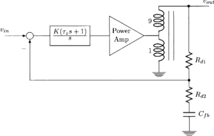
Vout
9
VIn K(Ts + 1) _ Power
Rd2
Cb
Figure 2-3: The circuit model for the PI controller and plant. vi" is taken from the output of the
multi-frequency source from the sensor board and v
0t drives the source plates directly.
As is shown in Figure 2-3, the input signal is gained up by a power amplifier and
autotrans-former with a PI feedback network. An autotransautotrans-former has several advantages over a two-winding
a feedback path to be wrapped around the transformer to the PI controller. An autotransformer
also requires less copper than its equivalent two-winding transformer. Finally, the autotransformer
is more efficient electrically. It experiences lower losses through the secondary leakage impedances
than a two-winding transformer.
Figure 2-4: The high voltage source board.
2.3
Sensing Circuitry
2.3.1
Front-end Amplifier
The receive electrodes, like the source electrodes, are copper planes on a printed circuit board. The
front-end amplifiers of the differential pair are placed on the electrodes themselves to prevent against
the parasitic capacitive loading of the sensing node by an undriven cable. The amplifier on these
active electrodes is configured as a transimpedance amplifier and thus will convert an input current
to an output voltage
Vo=
(Rf-in
.
(2.1)
The input current is provided by the signal source, vin, and the sensed capacitance to the receive
electrode, Cen, by
iin = Vin = Vin " sen.
Ie~
Ru 57 II Ie Icq 22 Dec I1302III:5II 8:0II 3 II
...
Chi 200rnY M 40.0ps 5.0GS&
A Ch1 r 424mnY Curs1 POs 800.Ons Curs2 Pos 96.58ps
0i:
800.Ons
Z 96.58 s AL: 95.78P 1/6: 10.44kHz Pk-Pk(C1) 976.Okrip:
974.35563rn m: 968.Orn M:984.On
a:
3.544m n: 57.0(a) The summed
T k. R H
sinusoids at the divided output of the high voltage source
107 A' 22~ D 1 3 71 I T-I -.. .I .. .. .-I si M 20.Oms 250kS/s 4.0psAx A Ch1 f 396mV
(b) FFT taken of the divided output of the high voltage source
Figure 2-5: These figures were taken from a single frame of a digital oscilloscope.
Curs1 POs
10.4kHz
Curs2 Pos
|-83.345kHz
1 1 4kH
Tek Run HI Res
57
Acis 22 Dec 1302:53:03
200"
Simplifying these equations gives us the theoretical relationship between the front-end transfer
func-tion and the sensed capacitance
Vo
0t
_
SRf Cen
(2.3)
vi,,
1+sRCf
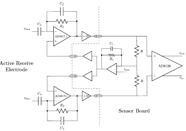
Another important aspect of this front-end is its common-mode feedback for common-mode
rejection. The electrodes are meant to measure the small changes in the differential signal between
them corresponding to a change in the occupation or location of materials in the space, and
common-mode signals must be rejected. To do so, the output from the active electrodes, given by
Vout
= Ad(v1 - v2)+
Acm (V1 + V22
(2.4)
is sent to the sensor board; the common-mode signal is then extracted and sent back to the active
electrodes to be canceled. A circuit diagram is presented in Figure 2-7 and the corresponding block
diagram in Figure 2-8.
Figure 2-6: A close-up of the front-end amplifier on one of the receive electrodes.
2.3.2
Signal Conditioning
Once the signal is received and its common-mode component is rejected, it is ready for processing.
The diagram in Figure 2-9 summarizes this three to four channel signal conditioning block. The
synchronous detector used in this sensor design collects both the in-phase and quadrature data from
the input to the front-end. To do so, the input signal is multiplied separately by a clock signal and
a signal
900
out-of-phase. Collecting in-phase and quadrature information reduces the impact of
any phase error between the input signal and the demodulating signals. The synchronous detector
Cf
CS
Vi" Rf AD4817-1 X10 'E vin+ Cc Rceive
de
__C.
IGc
CC AD4817-1 XSensor Boar
Cf vo+ AD8138vo_
Figure 2-7: Schematic for the half circuit common mode feedback of the front end amplifier. Feedback
capacitances represent lumped T-networks. Electrode circuitry is left of the cable and sensor board
circuitry to the right.
Interference
Fig 2:
B
k d
g
H
-x 10
Figure 2-8: Block diagram for the common mode feedback of the front end amplifier.
Active Re
Electro
is realized with the MAX4523. This set of analog switches is configured in a full bridge topology and driven by the in-phase s and quadrature s clock signals to form a square wave multiplier as in Figure 2-10. The 900 phase shift between multiplier clock signals is generated by a chain of D flip
flops.
Vinl G1
-Synch. Det. Instr. Amp.
G2 G3 0 & -+ & I b
LPF ADC
ii
Vin2 G,
--x4
Figure 2-9: The generalized block diagram for the signal conditioning circuitry. The first gain stage is singled ended and located on each respective electrode. The following stages are all fully differential and reside on the sensor board. The dashed box is replicated four times.
The passive low-pass filter block following the multiplier suppresses unwanted high frequency content. The filter poles have been placed according to a compromise between settling time and multiplier ripple aliasing rejection.
Vin+ 0-V -Figu '
VOWt,+
| |I MA X4523 - -EA
PC SADCPC
r2 I---ire 2-10: One-channel circuit implementation of the synchronous demodulator.
Next the AD8230, an instrumentation amplifier, converts the differential signal to single-ended
and adds a reference voltage. It does so to shift the signal to the middle of the analog-to-digital
(ADC) converter rail. A configurable gain may also be added to make use of its full range. Finally,
the output of the instrumentation amplifier is sent to the ADC. The LTC2484 is a 24-bit E-A ADC
with an SPI interface for sampling and reading from the converter. A photo of the sensor board with
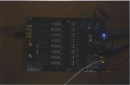
four channels (two frequencies with in-phase and quadrature information) is shown in Figure 2-11.
Figure 2-11: The sensor board with DDS signal creation in the bottom-right corner, microcontroller
breakout in the center-right and demodulation signal creation top-right. The front-end amplifier is
at the input to the board on the left. The signal is delivered to the board from the active receive
electrodes via driven coaxial cables to the MMCX connectors.
2.4
Circuit Changes
Since Version 2.0 of the sensing circuitry, there have been several changes made to cut out extraneous
hardware and add extra capabilities to the system.
2.4.1
Signal Conditioning
Along the signal conditioning path, a second differential pair of channels was added to provide the
ability to add a second pair of receive electrodes. Jumpers are used to allow either a second electrode
pair or a divided source signal input to collect drift and noise measurements.
The potentiometers at the output of the AD8230 instrumentation amplifiers were also removed
to allow for the placement of matching resistors to set the gain of this amplifier. The gain, given by
g
2
1+
RF)(2.5)
RG
can be calculated to take advantage of the full input range of the ADC. The adjustable delay
blocks before the flip flops were also removed because they were unnecessary. The relative phase
delay between the DDS-derived source signal and the in-phase demodulation signal is unimportant
because the delay introduced between the DDS signal and the received signal is unknown. Also, when
of phase delay.
2.4.2
Signal Synthesis
In the signal synthesis block, several parts were removed or replaced to cut down the total BOM cost and reduce complexity. The resistor reference summed with the two DDS outputs in Revision 2.0 was replaced here with an op-amp buffer reference. Without the op-amp buffer, the reference (used to subtract the combined dc offset from the summed DDS outputs) would be sensitive to changes in the gain of the summing amplifier. This would mean that without the gain of 10 originally used in this circuit, a dc offset whose value is scaled by this gain would be added to the summed sine waves from the DDS.
2.4.3
HV Selection
To multiplex the three high voltage source electrodes, a National Instruments DAQ device was used with high voltage, RF relays to switch the input signal between possible combinations of electrodes. Three relays were used in series to increase the standoff voltage to 200 x 3 = 600V. This left plenty of room for the high voltage maximum amplitude of 500 V. The NI-DAQ device was controlled with a Matlab interface. Each of three digital outputs were toggled in binary order to create seven possible combinations of source electrodes, and one "off" state.
Vout
+ Vd,
VNI
Vin
Figure 2-12: Schematic for one channel of the high voltage source multiplexer board. Three relays are stacked in series to standoff the 500 V peak voltage.: The remaining two channels and shield switches are not shown.
Two issues arose while creating the final source setup. First, coupling was causing a signal to appear on source electrodes that were supposed to be switched off. Second, unwanted oscillation of
Table 2.1: Stray capacitance measurements at 100kHz
Rev.
Cnii
Cin2 Cin3 Cgndi Cgnd2 Cgnd3 C1 2 C23 C131.0
3 pF
2.71 pF
2.68 pF
7.3 pF
6.46 pF
6.35 pF
2.23 pF
1.97 pF
2.15 pF
2.0
0.25 pF
0.23 pF
0.23 pF
0.2 pF
0.18 pF
0.18 pF
0.08 pF
0.08 pF
0 pF
the source would occur when all electrodes were connected.
To solve these problems, several important layout and wiring changes were made. First, the
source multiplexer board was rebuilt on unplated perfboard and all components were soldered
to-gether with short pieces of wire wrap wire. Layout changes were also made. The three relays for
each channel were placed close together in series with 2" separations between each channel. The
shields of the output connectors were also switched with three relays in series and a 1" separation
was left between each channel and its respective shield. Finally, a distance of about 5" was left
be-tween the closest output and the input. With these changes made, there was an order of magnitude
improvement in stray capacitance as illustrated in Table 2.1.
Next, a ground plane in the form of a long piece of copper tape was added across the outputs of
the multiplexer board to shunt any source radiation from the input connector to the board. This is
to prevent any coupling from input to output on each channel. The new board revision is shown in
Figure 2-13.
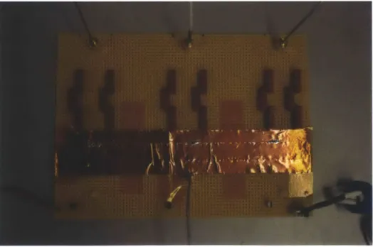
Figure 2-13: Revision 2.0 of the high voltage multiplexer board. Large separation between channels
and input and output provided a significant reduction in coupling capacitances.
the multiplexer board through the cable carrying the digital output signals from the NI-DAQ box,
USB isolators were added between the NI-DAQ box and the computer, and the computer and the
sensor board. Ferrite beads were positioned around the circuit to suppress EMI.
The NI-DAQ box was also moved next to the high voltage source. The NI-DAQ cable was
originally fed across the room along the floor about 15', adding an unshielded coupling path for the
source signal. With the NI-DAQ box close to the source, the signal transmission path is almost
solely along an isolated, well-shielded USB cable, blocking a previous source of coupling.
2.5
Setup
There are several experimental setups used in this thesis. The primary configuration of electrodes
in the lab space is shown in Figure 2-14
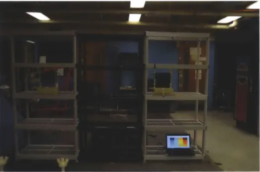
Figure 2-14: Receive electrodes placed on plastic shelves in the lab space. Sensor electronics are
beyond the shelves on the ground and source electrodes are on a table across the lab space.
Chapter 3
Passive Scanning
3.1
Analog Demodulation
When used without an active source, this system becomes a "passive scanner." By sweeping the
demodulation frequency, the contribution of asynchronous, independent sources within the frequency
range of the sensor (such as fluorescent lamps, laptop drives, etc.) can be determined. Unfortunately,
there are several issues with using an asynchronous demodulation signal. These issues and several
solutions are discussed here.
In the test depicted by Figure 3-1, an independent source was created using our source boards and
a function generator. Because this source is not synchronous with the detection circuit, it provides
a way to observe and study the effect of a controlled asynchronous source on the sensor. This source
was placed across the room and its signal was then picked up by our receiver and demodulated
using a separate function generator. The demodulation frequency was tuned by hand to be closest
to the source frequency, as in Figure 3-2. Here, only the difference in frequency between the source
and receive frequencies matters as all phase information is contained in the IQ measurements. The
difference or "beat" frequency between the independent source and demodulation frequencies is
defined as
A
2A cos(2rrfit)
xA cos(2rrf
2t) =2 (cos(2rr(fi + f
2)t) + cos(2rr(fi
-f
2)t))
(3.1)
where the difference frequency is given as
fbeat = Ifi -
f21.
(3.2)
The bandwidth of the low-pass filter after the demodulation block is not low enough to attenuate
this beat frequency so it is passed to the input of the ADC. Therefore, the digital output of the
vi(s)
High Voltage Differential Front-endv,.(S)
0 Source EActrives Amplifier
User variable in-put demodulation
frequency from signal generator
Figure 3-1: Block diagram of manual demodulation tuning test.
ADC is no longer entirely DC as shown in Figure 3-3.
a) a) L) 2.7
2.6
2.5
2.4 2.32.2
2.1
2
1.9
1.8
1 7x
10-
Tuning Demodulation Frequency to Independent Source
0
1020
30
40
50
60
Time (s)
Figure 3-2: Gradually
source frequency.
increasing the demodulation frequency to within 0.01 Hz of the independent
Another factor effecting the ability to precisely demodulate an asynchronous source such as a
fluorescent lamp is source frequency drift. Fluorescent lamp switching frequencies in the laboratory
space range from 26 kHz to 49 kHz and have exhibited frequency drifts of at least t 1 Hz. It becomes
very difficult to demodulate a drifting source without a synchronous receive signal.
3.2
Spectrum Analyzer
A real-time spectrum analyzer (RTSA) was used with our active electrodes and front-end amplifiers
to analyze the frequency content of the lab space. Table 3.1 shows the various distinct peaks we
-. -. . . . -.
-. ..-. ....-. .... -. .
0) 0) 0 0) 0) 0 0) 0) 0) 0~ C
6
5
4
3
2
1
0
-1
-2
-31
0
X 10
3Difference Frequency with Independent Source
=400kHz
200
400
600
800
1000
Time (s)
Figure 3-3: With the demodulation
frequency is observed over time.
1200
1400
1600
1800
frequency within 0.01 Hz of the source frequency, the beat
space and by approaching each bank with a oscilloscope probe with pick-up loop the peak size at
each frequency was matched with its physical location in the room.
The spectrum analyzer used was the Tektronix RSA3303A 3GHz Real-time Spectrum Analyzer.
All figures below were captured in single-shot trace mode.
Vi
(S) High Voltage Differential FRont-end Vsa (S)Source Acl tives Amplifier
Figure 3-4: Block diagram of manual demodulation tuning test.
3.3
Applications
This "passive scanner" could be an excellent companion to previous non-intrusive load monitoring
capabilities developed by Professor Steven Leeb. Our sensor provides the ability to observe the
frequency characteristics and amplitude of various high voltage electrical sources in an area with no
electrical contact required. By replacing the spectrum analyzer in this system with the electronics
described in Section
7,
we would avoid the problems of asynchronous detection described above.
Additionally, this scanner could be used in conjunction with our hyperspectral EIT techniques.
By locking onto one of these sources and observing changes in signal amplitude when various objects
.. .. . . . ... .. . .... . .. .. .
.. . . . .
...
.... ...
..-
.
...
Power Spectrum Fluorescent Lamp
...
.
.
-.
... ..
-30
-40--50
-60 -- --70 - - - . -. --80-.-.--9
0..
... ..
...
.. .... . ..
. .
-100 - - - -.-..- .-110
2.35 2.4 2.45 2.5 2.55 2.6 2.65 Frequency (Hz) 2.7 2.75 2.8 2.85 x 10(a) Left Fluorescent Lamp at 26.54 kHz, RBW = 5 Hz
Power Spectrum Fluorescent Lamp
4 4.12 4.24 4.36 4.48 4.6 4.72 4.84 4.96 5.08 5.2
Frequency (Hz)
x 104 (b) Front and Back Fluorescent Lamps over 41-49 kHz, RBW = 10 Hz
Figure 3-5: These figures were taken from a single frame of the spectrum analyzer front-end amplifier and electrodes.
used with our
E 0 0L
-10
0 CL -20-30
-40
-50
--60
--70
-80
--90
-Mn
...
...
...
-.
..
.
.
...
.
.
.
-. . . . . . . . .....
. . . . . . . . . ... ............ .--. ..-. .- . ..--
....
-
. ...
.. .
. . . .-..
-... -.... -..-. --.. . ... ..... ..En M CD CL En M0 CD
Power Spectrum Laptop Touchpad
-70 -75 . --80 - - --85 - -.--90 --95 -100 - --105 -110 -.--115 ---1 5 -40 -50 -60 -70 -80 -90 -100 .2 5.21 5.22 5.23 5.24 5.25 5.26 5.27 5.28 5.29 5. Frequency (Hz) x 10
(a) Laptop Touchpad Signal at 52.53 kHz, RBW 10 Hz
Power Spectrum Laptop Hard Drive
....-.
.--.
... ..-.
..
-.
.
.
-.
..-.
..-
--
..
.-.
-.
--.
.... .... ..
.. ... .
-.
.
.
..
6.6297 7.0598 7.4898 Frequency (Hz) 7.9199 3 8.35 x 10 (b) Laptop Hard Drive Signal at 68.77 kHz, RBW = 50 HzFigure 3-6: These figures were taken from a single frame of the spectrum analyzer used with our front-end amplifier and electrodes. The laptop was placed on the same shelf as the left-side electrode.
Power Spectrum Second Harmonics -50 -55 - --60 -- ----65
---T
-70 - - ----
-7 0
..
...
...
.
..
. .
-..-.-.-
.
-~-80
-90--95 --100--- ---1058.35
8.7801
9.2102 9.6402 10.0703 Frequency (Hz) x1(a) Fluorescent Lamps Second Harmonics, RBW= 50 Hz
Power Spectrum Third Harmonics -G0 -55 -60 -.-.-.--65
T
-70 - -- --- ---83 -75 S-85 --95 ----100 1.23
1.275 1.32 1.365 1.41 1.455 1.5 Frequency (Hz) x 104(b) Fluorescent Lamps Third Harmonics, RBW 50 Hz
Figure 3-7: These figures were taken from a single frame of the spectrum analyzer used with our front-end amplifier and electrodes.
Table 3.1: Lab Space Independent Source List Frequency (kHz) Power (dBm) Identity 26.54 -39.5 Left Lamp
42.09
-42.6
Back Lamp
43.77-45.74 ~-42 Back Lamp 45.74 -20.73 Front Lamp47.13-48.73
~-44
Front Lamp
68.77
-43.17
Laptop HDD
52.53 -46.95 Laptop Touchpadare introduced into the lab space, the same image reconstruction could be performed without the
need for our own HV source. Preliminary experiments showed a roughly 10dB change in signal of
the closest fluorescent lamp as a person moved along the 2 meter horizontal marker in front of the
receive electrodes.
Chapter 4
Hyperspectral Imaging
4.1
Background
Many products and systems have used capacitive technologies for touchless sensing as discussed
in Chapter 1. However, this technology's unique ability to distinguish between different types of
materials present in an area using hyperspectral detection has not been realized in its current
ap-plications. This ability stems from the different permittivity responses as a function of frequency in
different materials, as shown in Figures 4-2 and 4-1. It is clear that while the conductivity of muscle
changes by orders of magnitude across this frequency range, the conductivity of aluminum is
rela-tively constant. Similarly, the relative permittivity of muscle changes dramatically with frequency,
while the relative permittivity of metals is 1 and is not frequency dependent. To take advantage of
this property, we drive our ECT system with several frequencies and are able to differentiate humans
from metal in a 100 ft2 area.
10"
10-0.3
10
5103
10
310
410
5106
Frequency (Hz)
Figure 4-1: The conductivity and permittivity of human muscle as a function of frequency [2,3].
Image reconstruction techniques are then used to locate objects. Ideally, the images produced
are sparsely populated in our 16-pixel space; this reduces the demands on reconstruction and allows
for accurate detection and differentiation of a small number of different objects in a larger space.
5.96
5.94
>
5.92
Q5.98
5.88
103
104
105
106
Frequency (Hz)Figure 4-2: The conductivity of aluminum as a function of frequency.
In this chapter, we present an ECT system operated at several frequencies which not only pro-duces a reconstructed image of the space occupancy, but provides information about the material composition of occupied areas.
4.2
Previous Work
First, a COMSOL Multiphysics model for the 2D system was created and capacitance data was derived as in a traditional ECT system described in Section 5.2. Matlab simulations were run then for various image reconstruction algorithms for use in an ECT system. These algorithms were compared using COMSOL test cases for interesting permittivity distributions. Figure 4-3 shows the modeled difference between the distributions of a test case of a human at two difference frequencies. Clever manipulations of the permittivity vs. frequency responses of different materials can lead to the differentiation of these materials when many types occupy one region.
X
-010
10 3
1 2 3 4 5 6 7 8 9 101
Figure 4-3: Difference between COMSOL-modeled human image at 100kHz and 20kHz To verify this, a simple proof-of-concept experiment was performed with help from post-doctoral
Original
2i
'IL
Table 1: Case 1: c, 80
LBP
Image Error: 0.962, Capacitance Residual: 1.0047, CC: 0.2103 Image Error: 1.0282, Capacitance Residual: 1.0074, CC: 0.14%
SVD
Figure 4-4:
rithms.
Landweber a=0.006 1000 iterationsImage Error: 0.7802, Capacitance Residual: 0.99M5, CC: 0.7363 1 Image Error: 0.9680, Capacitance Residual: 0.9996, CC: 0.8261
A COMSOL-modeled test case distribution with solutions by the LBP and SVD
algo-Image Error: 0.7676, Capacitance Residual: 0.9978 CC: 0.9347 algo-Image Error: 0.9787, Capacitance Residual: 0.9996, CC: 0.7404
box shielded by grounded aluminum foil. Inside, four plastic boxes represented four "pixels" which
could be filled with air (empty), distilled water or solid wood blocks. The box containing the pixels
was surrounded by four copper foil electrodes. Using a impedance analyzer, the capacitances between
each pair of electrodes were found. With the capacitance matrix and sensitivity matrix construction
described in Section 5.2, the inverse problem involving these matrices was solved to produce the
distribution shown in Figure 4-6b. In this experiment pixels 1 and 4 were filled with water and
pixels 2 and 3 were filled with wood. By taking measurements of the discrete distribution at two
different frequencies, 10 kHz and 100 kHz, the location of the water in the setup could be reproduced
by using the information from both data sets in the inverse problem solution.
G(100kHz)-G(10kHz) 0.M 0 -0.02 -OM raw# 3
(b) Resulting difference between
per-(a) Experimental test case
mittivity distributions
Figure 4-6: The experimental setup and test case for hyperspectral ECT. In this test case, pixels 1
and 4 were filled with water and pixels 2 and 3 were filled with wood. On the right, the difference
between the permittivity distributions at 10kHz and 100kHz.
Chapter 5
Imaging Techniques
This chapter will discuss the theory of tomographic imaging and the algorithms employed in this research. Given prior knowledge about the nature of the of the space, it is much easier to narrow down the possible solutions to an ill-posed inverse problem and pick a "most-likely" solution.
5.1
Setup
First, an experimental setup was constructed so that absolute position of objects in the space could be precisely recorded. Between the two rows of electrodes (three source plates and one differential pair of receive plates) the floor tiles formed a 4 x 4 grid. Each group of 4 tiles formed a square and each square marked a pixel in the vector representing the occupancy of the space. Objects were positioned in the middle of each square while data was collected.
5.2
Theory
In this section, the theory behind conventional electrical capacitance tomography (ECT) systems is described. Our approach to this problem is to abstract away the physics and use a binary occupancy value that will be described in Section 5.3.
To derive the capacitances between two electrodes relative to ground, we can first express the charge on each electrode as a linear combination of the voltages on all electrodes. The coefficients of these combinations are known as the coefficients of capacitance, and can be expressed in terms of the circuit capacitances. In a system with two electrodes, the measured capacitances of the circuit
X direction
_____ p
!
r2x
4X
16S1
S2 32 _Figure 5-1: The 4x4 grid in 2D space used as the spacial reference for all imaging.
Figure 5-2: Partial image of the 4x4 floor grid used for all experiments.
C0
x1
X
1 3are related to the charges and voltages of the electrodes in the following way:
Q1 = c11V1
+
c12V2(5.1)
Q2 = c21
V
1+
c2 2V
2(5.2)
Because of the symmetry of the problem, C12 = C21, meaning that there are only three unique
coefficients. Q1 = C
+
0G C1 2(V1 - 72) =(CIG
+ C12) V1 - C122 (5.3)Q2
=C2G2
+C
1 2(V2 - VI) = -0121 1 (02GC12)2
(5.4)
C1 = C1G+
012
(5.5)
C12 = -C12(5.6)
C22 = C2G +012
(5.7)
Finally, it becomes clear that the coefficients of self-capacitance, cil etc., provide no new infor-mation about the system and thus are generally ignored in our calculations.
The capacitance is measured by sending an ac signal to the source electrode and grounding the receive electrode. The induced current from the receive electrode is proportional to the actual capacitance between the two plates I, = jwVC, including any intervening dielectric material.
To retrieve the original permittivity distribution from these capacitance measurements, it is necessary to solve an inverse problem. An inverse problem is one that requires a solution for x in the matrix equation Ax = b. With an overdetermined or underdetermined system, this problem becomes impossible to solve exactly because A has no inverse. Indeed, ECT most often presents underdetermined problems because of the nature of the setup. In ECT systems, the unknown values are the permittivitties of each pixel in the desired image and the known values are the capacitances measured as detailed above. Thus, the inverse problem can be described by the equation Sg = c where c is a vector containing all capacitance measurements, g is the vector of unknown permittivities and S is a sensitivity coefficient matrix which linearly relates these values. To calculate the sensitivity matrix for a particular configuration, a function of the space and range of permittivities desired, the pixels of the space are individually filled with blocks of the material one wishes to sense. Solving for each value in the sensitivity matrix individually as in this 3 pixel, 2 electrode system gives
12
AC1 2 AC1 2 AC2T I==[AE1 AE2 AE3 I AC12 Ac1S
11-I
AC12mAci
AC12mAE
1Here, the complete result is a superposition of the results of filling each pixel with a dielectric
permittivity. The configuration is first measured "empty" and a displacement current I, is observed.
Subsequently, each pixel is filled one-by-one and the changes in current corresponding to changes in
capacitance are recorded and used to fill in the sensitivity matrix: Im
-1, = jWV1AC1
2 m.Once the
sensitivity matrix for a given configuration is calculated, an inverse problem, as described above, must
be solved to find the permittivity distributions from the sensitivity matrix and given capacitance
measurements. Various methods of choosing these distributions for underdetermined systems are
discussed in Section 5.5.
A6
1 [EAC12 AC1 2]QlaX
A1
[AC
12I
AC12
AE2 AE3Ac
AE
3 I I -II L IL--Ac,-f I. = I -A , -4= IV (a Cluain tesnivtym ixAd
A S=jrol AC
1(b) Superposition of all pixels
filled
Figure 5-3: On the left, individual pixels are filled with dielectric material to calculate the values of
the sensitivity matrix. On the right, the result of the superposition of all pixels is shown.
5.3
Forward Problem
In our forward model, we would like to abstract away the physics described above. It is easier to
etc. of an object in the space respectively. Thus, each x value represents a value we will henceforward
call the "occupancy" of each pixel, which is a function of many parameters. Our goal is detection,
defined as the ability to determine which pixels in a space are occupied, and eventually, by which
material. Here we will focus solely on detection of occupancy. In Chapter 4 material detection will
be discussed.
The linear system relating system voltage measurements and occupancy is given by
Ax = y
with
xi
c
0,
1
(5.8)
(5.9)
where A is an m x n sensitivity matrix, x is the
n
x 1 pixel occupancy vector and y is the m x 1
measurement vector. Specifically, in our experiment as described in Section 2.5
a1,1 a2,1 a3,1 m,1 a1,2 a2,2 a3,2 am, a1,3 a2,3 a3,3 am,1 -. - l,n ... a2,n ... a3,n ... am,1 X2
22
X 3 X n/
Y1 Y2 Y3 YmThe A matrix is filled column-by-column from the calibration measurements using single pixel oc-cupancy; i.e. if only pixel x1 is filled, the equation becomes
![Figure 2-1: A lumped element model for the capacitive sensor system [1].](https://thumb-eu.123doks.com/thumbv2/123doknet/13878098.446571/19.918.250.632.588.838/figure-lumped-element-model-capacitive-sensor.webp)